
Advance
SP8110
Rev 0.1 (12-03-03): SP8110 ≠ Two-Channel Modulation IC
SIPEX RESERVES THE RIGHT TO MAKE CHANGES TO THIS DATASHEET. CALL FOR UPDATES: 1-978-667-8700.
SIPEX CONFIDENTIAL, PRELIMINARY & PROPRIETARY. DO NOT DISTRIBUTE
OR COPY
page
1
of
3
1
2
3
4
8
7
6
5
IA
IB
Rf
Vcc
Vcc-out
LD_A
GND
LD_B
SP8110
FEATURES
∑ 5V Single supply voltage
∑ Two output channels, suitable for different
wavelength laser diodes
∑ Oscillator frequency is adjustable in both
channels simultaneously
∑ Oscillator amplitude is adjustable for each
output separately up to 130mA
∑ Operates two grounded laser diodes
∑ Small DFN 2 x 3mm package
APPLICATION
∑ DVD-ROM or DVD-Video applications utilizing twin laser diodes
GENERAL DESCRIPTION
The SP8110 is a Two-Channel Modulation IC utilizing high frequency current to suppress the
noise of grounded laser diodes. Modulation frequency is adjusted in both channels
simultaneously by an external resistor Rf tied to the ground. The amplitude of the high
frequency current is set for each channel separately by a DC input current applied to the
appropriate input pin (IA or IB for Laser A or Laser B, respectively). Current gain from input to
output is 100mA/mA (typical).
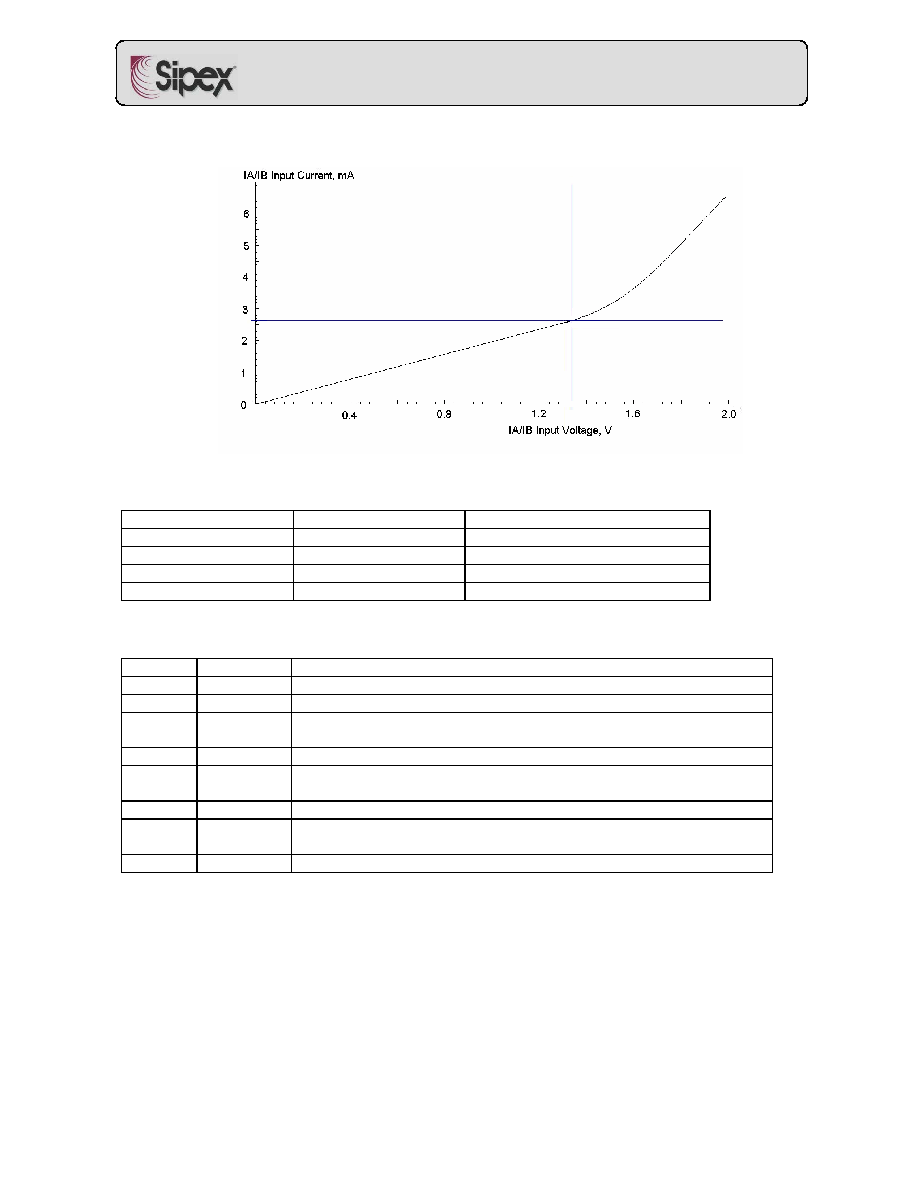
The input current at pins IA and IB is monitored to determine which channel is active. In the
event input current in both channels is below the active threshold level (approximately 2.65mA),
the SP8110 will enter Power Save mode. In the event a valid input current above the active
threshold level is present on both inputs, an Error mode is assumed and the outputs of both
channels are disabled. Supply current levels in Power Save and Error modes are below 0.2 and
0.8 mA respectively (maximum values).
The SP8110 is manufactured in 0.5/0.6 µm CMOS technology.
Two-Channel Modulation IC for Laser Diode
Advance
SP8110
Rev 0.1 (12-03-03): SP8110 ≠ Two-Channel Modulation IC
SIPEX RESERVES THE RIGHT TO MAKE CHANGES TO THIS DATASHEET. CALL FOR UPDATES: 1-978-667-8700.
SIPEX CONFIDENTIAL, PRELIMINARY & PROPRIETARY. DO NOT DISTRIBUTE
OR COPY
page
2
of
3
INPUT CHARACTERISTICS: IA/IB INPUT CURRENT VS INPUT VOLTAGE
MODE SELECTION
IA current
IB current
Mode
> 2.65 mA
< 2.5 mA
LD_A output active
< 2.5 mA
> 2.65 mA
LD_B output active
> 2.65 mA
> 2.65 mA
Error
< 2.5 mA
< 2.5 mA
Power Save
PIN ASSIGNMENTS
Pin No.
Pin Name
Function
1
IA
Amplitude setting for output LD_A
2
IB
Amplitude setting for output LD_B
3 R
Freq
Modulation Frequency adjusting pin
(An external resistor is connected between this pin and ground.)
4
Vcc
Power supply pin
5
LD_B
Output pin of channel B
(Anode of laser diode is connected with this pin.)
6 GND
Ground
pin
7
LD_A
Output pin of channel A
(Anode of laser diode is connected with this pin.)
8
Vcc_out
Power supply for LD_A and LD_B outputs
BOARD LAYOUT AND GROUNDING
To obtain the best performance from the SP8110, a printed circuit board with ground plane is
required. High quality, low series resistance ceramic 0.1uF bypass capacitors should be used at
the Vcc and Vcc_out pins (pins 4 and 8). Pin 8 should also have a 0.1uF bypass capacitor.
These capacitors must be located as close to the pins as possible. The traces connecting the
pins and the bypassing capacitors must be kept short and should be made as wide as possible.
Advance
SP8110
Rev 0.1 (12-03-03): SP8110 ≠ Two-Channel Modulation IC
SIPEX RESERVES THE RIGHT TO MAKE CHANGES TO THIS DATASHEET. CALL FOR UPDATES: 1-978-667-8700.
SIPEX CONFIDENTIAL, PRELIMINARY & PROPRIETARY. DO NOT DISTRIBUTE
OR COPY
page
3
of
3
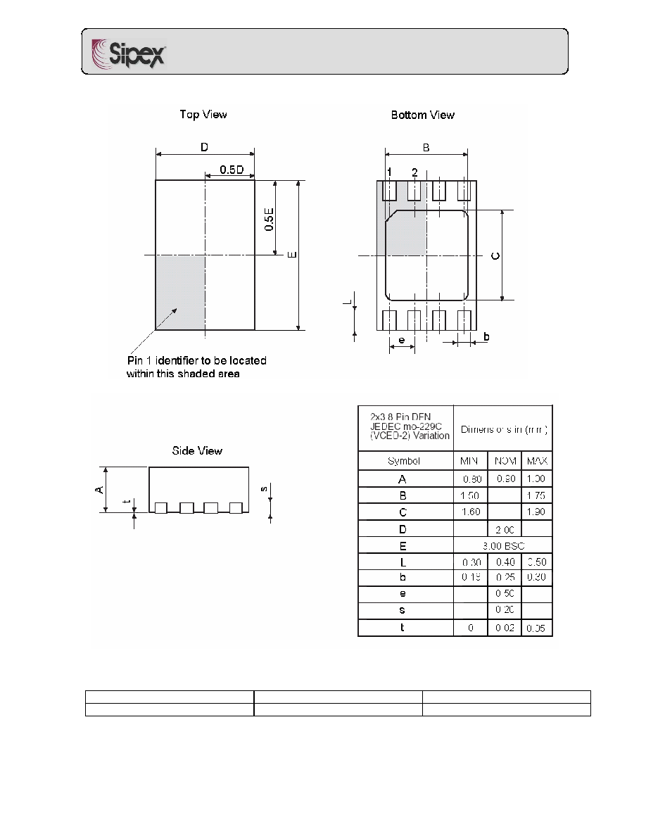
DFN 8-PIN PACKAGE DIMENSIONS
ORDERING INFORMATION
Part number
Temperature range
Package Type
SP8110ER
-40 to + 85
0
C
DFN 2 x 3 mm 8-pin