
1
Rev:B Date: 3/18/04
SP8126B High Speed Differential APC Amplifier
© Copyright 2004 Sipex Corporation
V
OUT+
TIA
Buffer
Buffer
R
GCOM
-
+
+
-
-
+
50pF
1k
50pF
1k
1V
P-P
(Flexible Flat Cable)
1V
P-P
R1
500
R2
500
R
G1
R
GAIN2
Gain Control
R
GAIN1
R
G2
GAIN
GND
V
OUT-
V
CC
R3
500
(Depend
on FPC)
High Speed Differential APC Amplifier
SP8126B
FEATURES
Dual Wavelength
Slew Rate of 300V/
µ
s
Fast Settling Time - 7ns
Gain Control
2V Output Swing
Low Offset Voltage: < 10mV
Low Offset Drift: < 20
µ
V/
∞
C
12dB External Gain Adjust Range
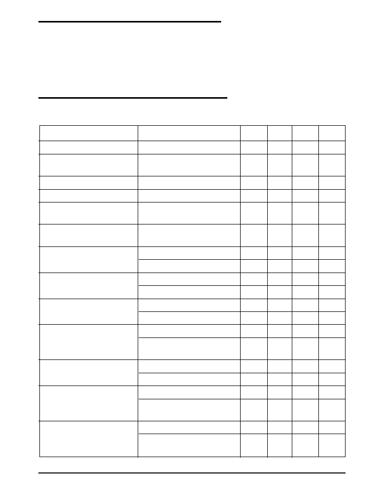
Figure 1. SP8126B Functional Diagram and Typical Application
DESCRIPTION
The SP8126B is a high-speed, differential output APC amplifier that integrates the photodiode
and adjustable gain block on one chip. Independent gain control allows individual adjustment for
780mn and 650nm wavelength operation, as found in CD/DVD optical storage drives. This allows
the user to control the laser power of the system in high-speed DVDRW, DVDRAM and CDRW
systems. The wide 2V output swing also allows better system performance, through improved
dynamic range.
APPLICATIONS
DVDRW
DVDRAM
CDRW
PRELIMINARY
1
2
8
7
6
5
3
4
GAIN
GND
V
CC
V
OUT
+
SP8126B
8 Pin COB
V
OUT
-
R
GCOM
R
GAIN1
R
GAIN2
2
Rev:A Date: 3/18/04
SP8126B High Speed Differential APC Amplifier
© Copyright 2004 Sipex Corporation
PARAMETER
CONDITIONS
MIN
TYP
MAX
UNITS
Supply Voltage
4.5
5
5.5
V
Output Sensitivity
Laser Beam Diameter = 0.70mm,
2400
3000
3600
V/W
uniform density
Output Sensitivity vs. Temp
R
GAIN
=1230
0.1
%/C
Output Sensitivity vs. Vcc R
GAIN
=1230
2
%/V
Input Optical Power Required
533
666
800
µ
W
to Produce 2V Output Swing
Full Scale Linear Output
2
2.8
V
Voltage Swing
Output Common Mode Voltage
2.3
2.5
2.7
V
4.5V < Vcc < 5.5V
Vcc/2.2 Vcc/2 Vcc/1.8
V
Output Offset Voltage
-10
0.5
10
mV
R
GAIN
= 1230
(High Gain)
-20
1.0
20
mV
Output Offset Voltage Drift
-25
-11
25
µ
V/C
R
GAIN
= 1230
(High Gain)
-50
-13
50
µ
V/C
Output Noise
BW = 100MHz
1.6
2
mVrms
BW = 100MHz,
2.4
5
mVrms
R
GAIN
= 1230
(High Gain)
Bandwidth
-3dB
70
100
MHz
-3dB, R
GAIN
= 1230
(High Gain)
50
68
MHz
PSRR
4.5V < Vcc < 5.5V
55
76
dB
4.5V < Vcc < 5.5V,
50
73
dB
R
GAIN
= 1230
(High Gain)
Output Settling Time(650nm) 2V
PP
Step
7
10
ns
(1% of Final Value)
2V
PP
Step,
12
15
ns
R
GAIN
= 1230
(High Gain)
ABSOLUTE MAXIMUM RATINGS
ELECTRICAL SPECIFICATIONS
Unless otherwise noted: V
CC
= 5.0V, C
LOAD
= 50pF to GND, R
LOADP
= R
LOADN
= 1k
to GND, R
GAIN
= 510
(Nominal Gain), -20
∞
C
T
A
+85
∞
C, Output measured differentially.
T
J(MAX) ........................................................................................
120
∞
C
V
S(MAX) ...............................................................................................
6V
V
IN(MAX) ..............................................................................................
6V
Power Supply Voltage
Continuous Power Dissipation (T
AMB
= 70
∞
C)
COB (derate 13.3mW/
∞
C above +70
∞
C) ......... 90mW
These are stress ratings only and functional operation
of the device at these ratings or any other above those
indicated in the operation sections of the specifications
below is not implied. Exposure to absolute maximum
rating conditions for extended periods of time may
affect reliability.
3
Rev:B Date: 3/18/04
SP8126B High Speed Differential APC Amplifier
© Copyright 2004 Sipex Corporation
PIN DESCRIPTION
PIN NUMBER
NAME
FUNCTION
1
V
CC
Supply Voltage
2
GAIN
Gain Select
3
R
GCOM
Common connection point for R
GAIN
1 and R
GAIN
2
4
GND
Power Ground
5
R
GAIN1
Gain Adjust 1 (Gain Select = LOW) or OPEN
6
R
GAIN2
Gain Adjust 2 (Gain Select = HIGH)
7
V
OUT
-
Output Voltage -
8
V
OUT
+
Output Voltage +
Internal Operation
The SP8126B APC circuit has an integrated
photo detector and is designed with nominal
sensitivities of 3mV/
µW for both 650nm and
780nm wavelength laser light. The part's sensi-
tivity can also be adjusted continuously and
independently for two different gain modes via
two external resistors over a range of
±6dB. The
two gain modes are controlled by a TTL com-
patible logic input, called GAIN SELECT. This
logic pin selects between the two external gain
setting resistors to allow independent control
and settings for the two gain functions.
The system is a two stage design, consisting of
a Trans-Impedance Amplifier (TIA) and an out-
put buffer stage. In dark condition the outputs
V
OUT
- and V
OUT
+ are set to a reference voltage
that is defined internally as Vcc/2. With 650nm
or 780nm wavelength laser light falling on the
photodetector, the output will swing differen-
tially around Vcc/2 proportional with the light
power according to the chosen gain.
TIA and Gain control
The first stage is a differential TIA used to
convert the photodetector current to a balanced
differential voltage. The traditional fixed feed-
back resistors have been replaced with an active
resistor circuit that sets the trans-impedance value.
A Resistor Control Block that senses the value
of the external gain setting resistor controls the
value of the equivalent feedback resistor.
PARAMETER
CONDITIONS
MIN
TYP
MAX
UNITS
Output Settling Time (780nm)
2V
PP
Step
10
13
ns
(1% of Final Value)
2V
PP
Step,
15
18
ns
R
GAIN
= 1230
(High Gain)
Output Slew Rate
200
300
V/
µ
s
Output Overshoot
2V
PP
Step
5
%
Power Supply Current
15
mA
-20
∞
C < T
A
< +85
∞
C
20
mA
Gain Adjust Range
225
< R
GAIN
< 1230
-6
6
dB
Gain Select Input Voltage
0.8
V
VIL (TTL Level)
Gain Select Input Voltage
2.0
V
VIH (TTL Level)
THEORY OF OPERATION
Unless otherwise noted: V
CC
= 5.0V, C
LOAD
= 50pF to GND, R
LOADP
= R
LOADN
= 1k
to GND, R
GAIN
= 510
(Nominal Gain), -20
∞
C
T
A
+85
∞
C, Output measured differentially.
ELECTRICAL SPECIFICATIONS: Continued
4
Rev:A Date: 3/18/04
SP8126B High Speed Differential APC Amplifier
© Copyright 2004 Sipex Corporation
The
±6dB Gain adjustment is therefore done
directly in the TIA, by adjusting the active
feedback blocks proportional with the gain set-
ting resistor. The external resistor is not directly
in the signal path, and therefore any parasitic
from the off-chip connections does not affect
the signal quality. The value of the active feed-
back is controlled tightly over supply and tem-
perature changes through a Control Block with
active feedback circuitry.
Gain control is proportional with the external
resistor, so the lowest value of R
GAIN
will pro-
duce the -6dB gain adjustment and the highest
value will produce the +6dB gain adjustment.
Please consult the specification table for the
required R
GAIN
values.
Buffer
This stage buffers the differential signal from
the TIA to the V
OUT
pins and refers the signal to
the internal reference voltage. A balanced cur-
rent feedback amplifier is used for this purpose
to achieve high slew rate and fast settling.
The buffer is designed to drive high capacitive
loads. The maximum load is 50pF bulk. The
actual load is typically a flexible printed circuit
(FPC) that acts like a transmission line. This
presents a distributed capacitive load plus in-
ductance and resistance. In this case care should be
taken to match the characteristic impedance of the
line at the far end to avoid standing waves and
ringing. The buffer is designed to drive 1k
to
ground. However, this resistor can be adjusted in
value to accommodate the characteristic imped-
ance of the signal trace. The output buffer ampli-
fier is designed to be stable without load and with
loads up to 50pF lumped capacitance.
THEORY OF OPERATION: Continued
180M
160M
140M
120M
100M
80M
60M
40M
0.0
250
500
750
1.0k
1.25K
1.5k
R
GAIN
-9.5dB
0.0dB
-6.0dB
(Hz)
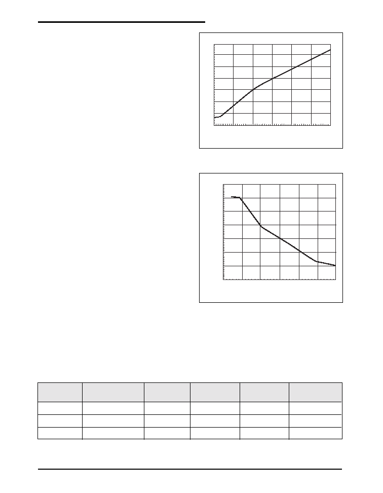
6 .0dB
Figure 3. Bandwidth versus R
GAIN
TABLE 1: APC SYSTEM TARGET GAIN SET POINTS.
V
OUTP
-V
OUTN
= 2V
P-P
, V
CC
= 5V, T = 27
∞C
Gain
Sensitivity
R
GAIN
Ts 1%
BW
Pin
(dB)
(V/W)
(
)
(nS)
(MHz)
(
µ
W)
+6
6000
1230
12
68
335
0
3000
510
7
119
666
-6
1500
225
5.5
160
1331
Figure 2. Sensitivity versus R
GAIN
7.0k
6.0k
5.0k
4.0k
3.0k
2.0k
1.0k
0.0k
0.0
250
500
750
1.0k
1.25K
1.5k
R
GAIN
5
Rev:B Date: 3/18/04
SP8126B High Speed Differential APC Amplifier
© Copyright 2004 Sipex Corporation
A major consideration in developing the optical
pick-up head system is the extremely small form
factor, which is additionally aggravated by the
physical locations required by the light path.
Special care must be taken when designing the
Flex or PCB for this part. The output peak
current requirement is in the order of 12.5mA
when driving 50pF of capacitive load with a
slew rate of 250V/
µs Therefore care must be
taken to provide low inductance, low resistance
paths for power and ground and output traces.
Supply coupling is also very important. Good
supply decoupling is important to ensure the
high frequency performance of the system by
eliminating supply lead inductance effects. The
decoupling capacitor C1, as shown in Figure 5,
should be as close to the part as possible. This
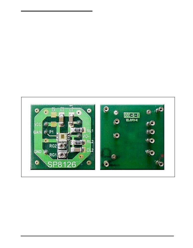
Figure 4. Test and Evaluation PCB Layout for COB 8 Lead Package
Top
Bottom
capacitor should be 0.1
µF ceramic. C2 is op-
tional to improve decoupling and is recom-
mended to be 1
µF tantalum. The layout of the
PCB is pictured here. Note the wide and short
traces on the supply lines.
The traces for the gain resistors R
GAIN1
and
R
GAIN2
are kept as short as possible to avoid
excessive parasitics. Any parasitics on these
nodes will limit the performance of the system.
R
GAIN1
and R
GAIN2
are subminiature potentiom-
eters in the application. This is a single layer
board using FR4 material.
In order to minimize coupling capacitance into
the gain setting resistor nodes, it is also critical
that V
OUT
+ and V
OUT
- are routed away from the
traces associated with the gain-setting resistors.
LAYOUT AND ROUTING CONSIDERATIONS