 | –≠–ª–µ–∫—Ç—Ä–æ–Ω–Ω—ã–π –∫–æ–º–ø–æ–Ω–µ–Ω—Ç: SP8130 | –°–∫–∞—á–∞—Ç—å:  PDF PDF  ZIP ZIP |
Rev 0.8 09/25/06. SP8130 High Speed Differential APC Amplifier 2006 Sipex Corporation
`````````
page
1
of
5
1
2
3
4
8
7
6
5
Gain
Rg1
Rgcom
Rg2
Vcc
Vout (+)
Vout (-)
Gnd
SP8130
8-Pin
OPLGA
FEATURES
∑
Dual wavelength 650 and 780nm
∑
160 MHz Bandwidth @ -6dB
∑
600 V/µs Slew Rate
∑
6 ns Settling Time
∑
10 mV Differential Output Offset Voltage
∑
30 uV/
o
C Output Offset Voltage Drift
∑
-6/+6 dB External Gain Adjust
∑
Small 8-pin OPLGA package
APPLICATIONs
∑
CD-R, and CD-RW
∑
DVD+/-R, DVD+/-RW, and DVD-RAM
GENERAL DESCRIPTION
The SP8130 is a high-speed, differential output APC amplifier that integrates the photodiode and
adjustable gain block on one chip. Independent gain control allows individual adjustment for 780nm
and 650nm wavelength operation, as found in CD/DVD optical storage drives. This allows the user to
control the laser power of the system in high-speed DVD+/-RW, DVD-RAM and CD-RW systems.
The wide 2V output swing also allows better system performance, through improved dynamic range.
Solved by
TM
SP8130
High Speed Differential APC Amplifier

Rev 0.8 09/25/06. SP8130 High Speed Differential APC Amplifier 2006 Sipex Corporation
`````````
page
2
of
5
ABSOLUTE MAXIMUM RATINGS
These are stress ratings only and functional operation of the device at these ratings or any other
above those indicated in the operation sections of the specifications below is not implied. Exposure to
absolute maximum rating conditions for extended periods of time may affect reliability.
Supply Voltage (Vcc).......................................6.0V
Reference Voltage (Vs) .................................. 6.0V
Output Voltage (Vout)...................................... Vcc
Junction Temperature (Tj)..............................120
o
C
Storage Temperature.......................-40∞C to +100∞C
Soldering Temperature................................+245∞C
(1x Reflow/MSL Level 6)*
* Based upon 500 temperature cycles as judgment criteria
RECOMMENDED OPERATING CONDITIONS
Supply Voltage (Vcc)...............................4.5V to 5.5V
Operating temperature..........................-20C to +85
o
C
CD Wavelength.............................................780nm
DVD Wavelength...........................................650nm
THERMAL SPECIFICATIONS
8-pin OPLGA (3 x 3.5mm) Package
Thermal Resistance..................................... 75
o
C/W
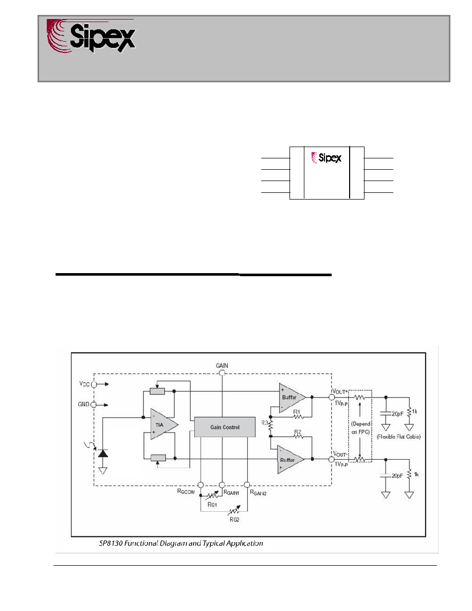
SCHEMATIC DIAGRAM

Rev 0.8 09/25/06. SP8130 High Speed Differential APC Amplifier 2006 Sipex Corporation
`````````
page
3
of
5
ELECTRICAL/OPTICAL SPECIFICATIONS
Unless otherwise noted: Vcc = 5V, output load: R
L
= 1k, C
L
= 20pF, gain 0 dB, ambient temperature -20C T
A
+85
o
C
Unless otherwise noted, electrical specifications apply to all gain modes.
Parameter
Condition
Min.
Typ.
Max
Unit
T
A
= 25
o
C, no signal
15
Supply Current
-20 T
A
+85
o
C, no signal
20
mA
Output Common Mode Voltage
No signal
Vcc/2.2
Vcc/2
Vcc/1.8
V
Gain = 0dB, no signal
-10
10
Output Offset Voltage
Gain = +6dB, no signal
-15
15
mV
Gain = 0dB, no signal
-30
30
Output Offset Voltage Drift
Gain = + 6dB, no signal
-45
45
µ
V/
o
C
Power Supply Rejection Ratio
(PSRR) *
Gain = 0dB, 4.5V Vcc 5.5V
-55
-80
dB
Logic level low
0.8
Gain Switch Input Voltage
Logic level high
2
V
Output Sensitivity
Gain = 0dB
5700
V/W
Input Optical Power required to
produce a 2V differential output
swing
0.28mm laser beam diameter,
uniform density, Gain = 0dB
350
µ
W
Photo Detector Active Area
0.25
mm
2
Output Sensitivity Change vs. Vcc
All gains
1
4
%/V
Output Sensitivity Change vs.
Temperature
All gains
0.05
0.1
%/
o
C
Gain = 0dB
1.6
2
Output Noise, BW= 100MHz
Gain = +6dB
2.6
5
mV
rms
Output Slew Rate
400
600
V/µs
Gain = -6dB, 2Vpp step, f=10MHz
6.2
7
Gain = -0dB, 2Vpp step, f=10MHz
7.0
8
Output Setting Time to
2%
of final
value
Gain = +6dB, 2Vpp step, f=10MHz
7.1
9
ns
Full Scale Output Voltage Swing
2
V p-p
Output Overshoot
All gains
0.5
2
%
Gain = -6dB, -3dB level
160
Gain = 0dB, -3dB level
140
MHz
Bandwidth
Gain = +6dB, -3dB level
120
Gain Adjust Range
-6
+8
dB
*) PSRR = 20log (Vcc/V
OUT
)
**) Gain Linearity = (Gain2 ≠ Gain 1)/Gain 1, where Gain = V
OUT
/Pin. This test is done with current injection at the wafer level.

Rev 0.8 09/25/06. SP8130 High Speed Differential APC Amplifier 2006 Sipex Corporation
`````````
page
4
of
5
PIN ASSIGNMENTS
Pin #
Pin Name
Pin Function
1
Gain
Gain Switch Input. Low level selects R
G
1, high level selects R
G
2
2
R
G
1
Gain Adjust 1
3
R
GCOM
Common connection point for R
G
1
and R
G
2
4
R
G
2
Gain Adjust 2
5
GND
Power Ground
6
V
OUT
(≠)
Output Voltage Negative Swing
7
V
OUT
(+)
Output Voltage Positive Swing
8
Vcc
Supply Voltage. Bypass to GND with ceramic capacitor 0.1µF
OPLGA 8-pin PACKAGE DIMENSIONS
Clear Mold Compound Characteristics:
Clear Mold Material : NT330HQ
Refractive index
: 1.57

Rev 0.8 09/25/06. SP8130 High Speed Differential APC Amplifier 2006 Sipex Corporation
`````````
page
5
of
5
PHOTO DETECTOR PATTERN
Tolerance of PD position:
X, Y: +/- 0.20mm
Angle: 0∞ +/- 1∞
Die tilt: 0∞ +/- 2∞
ORDERING INFORMATION
Part Number
Temperature range
Package Type
SP8130DG4
-20C + 85
0
C
8-pin OPLGA