 | ÐлекÑÑоннÑй компоненÑ: SP8480JP | СкаÑаÑÑ:  PDF PDF  ZIP ZIP |
Äîêóìåíòàöèÿ è îïèñàíèÿ www.docs.chipfind.ru
289
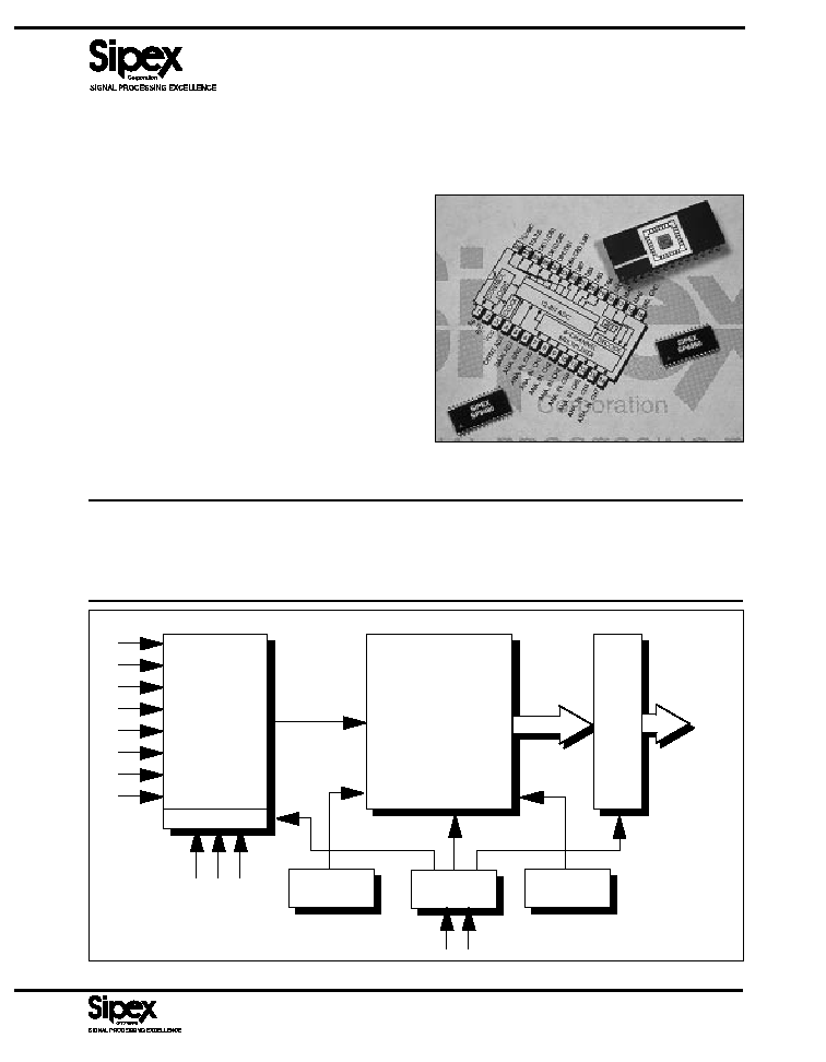
CONTROL
LOGIC
MULTIPLEXER
8BIT/4BIT NIBBLE
OUTPUT
CLOCK
REFERENCE
12-BIT A/D
CONVERTER
MUX DECODE
DESCRIPTION...
The SP8480 Series are complete monolithic data acquisition systems, featuring 8-channel
multiplexer, internal reference and 12-bit sampling A/D converter in 28pin plastic DIP or SOIC
packages. Linearity errors of
±
0.5 and
±
1.0 LSB, and Differential Non-linearity to 12-bits are
guaranteed, with no missing codes over temperature. Multiplexer settling plus acquisition time
is 1.9
µ
s maximum; A/D conversion time is 8.1
µ
s maximum.
s
Complete Monolithic 8-Channel, 12-Bit
DAS
s
100kHz Throughput
s
16-Bit Microprocessor Bus Interface
s
MUX Inputs Overvoltage Protected
s
Parallel 8/4-Bit Nibble Output
s
Tri-State Latched Output
s
No Missing Codes to 12-Bits
s
28-pin SOIC and PDIP package
s
200mW Max Power Dissipation
(140mw Typ.)
*Formerly part of the SP410 Series.
SP8480*
Monolithic, 12Bit Data Acquisition System
290
ABSOLUTE MAXIMUM RATINGS
V
CC
to Common Ground ............................................... 0V to +16.5V
V
LOGIC
to Common Ground .................................................. 0V to +7V
Analog Common to Digital Common Ground ............... -0.5V to +1V
Digital Inputs to Common Ground ...................... -0.5V to V
LOGIC
+0.5V
Digital Outputs to Common Ground ................... -0.5V to V
LOGIC
+0.5V
Multiplexer Analog Inputs ...................................... -16.5V to +31.5V
Gain and Offset Adjustment ................................. -0.5V to V
CC
+0.5V
Analog Input Maximum Current ............................................. 25mA
Temperature with Bias Applied ............................. -55
°
C to +125
°
C
Storage Temperature ............................................ -65
°
C to +150
°
C
Lead Temperature, Soldering .................................... 300
°
C, 10sec
SPECIFICATIONS
(T
A
= 25
°
C and nominal supply voltages unless otherwise noted)
MIN.
TYP.
MAX.
UNIT
CONDITIONS
ANALOG INPUTS
Input Voltage Range
0 to +5
V
Multiplexer Inputs
8
Configuration
Single-ended
Input Impedance
ON Channel
10
9
Parallel with 30pF
OFF Channel
10
10
Parallel with 5pF
Input Bias Current
Per Channel
±
10
nA
25
°
C
±
250
nA
-55
°
C to +125
°
C
Crosstalk
OFF to ON Channel
-90
dB
10kHz, 0V to +5V
pk-to-pk
-80
dB
50kHz, 0V to +5V
pk-to-pk
-70
dB
100kHz, 0V to +5V
pk-to-pk
ACCURACY
Resolution
12
Bits
Linearity Error
K, B
±
0.5
LSB
J, A
±
1
LSB
Differential Non-Linearity
K, B
±
1
LSB
J, A
±
2
LSB
Offset Error
±
2
LSB
Adjustable to zero
Gain Error
±
0.3
%FSR
Adjustable to zero
No Missing Codes
K, B
Guaranteed
TRANSFER CHARACTERISTICS
Throughput Rate
100
kHz
MUX Settling/Acquisition
1.9
µ
s
A/D Conversion
8.1
µ
s
STABILITY
Linearity
±
0.5
±
2.5
ppm/
°
C
Offset
±
5
±
25
ppm/
°
C
Gain
±
10
±
50
ppm/
°
C
DIGITAL INPUTS
Capacitance
5
pF
Logic Levels
V
IH
+2.4
+5.5
V
V
IL
-0.5
+0.8
V
I
IH
±
5
µ
A
I
IL
±
5
µ
A
291
SPECIFICATIONS
(T
A
= 25
°
C and nominal supply voltages unless otherwise noted)
MIN.
TYP.
MAX.
UNIT
CONDITIONS
DIGITAL OUTPUTS
Capacitance
5
pF
Logic Levels
V
OH
+2.4
V
I
OH
500
µ
A
V
OL
+0.4
V
I
OL
1.6mA
Leakage Current
±
40
µ
A
High impedance, data bits only
Data Output
Offset Binary
POWER REQUIREMENTS
V
LOGIC
+4.5
+5.5
V
I
LOGIC
0.8
4
mA
V
CC
+11.4
+16.5
V
I
CC
9
12
mA
Power Dissipation
140
200
mW
ENVIRONMENTAL
Operating Temperature
Commercial; J, K
0
+70
°
C
Industrial; A, B
-40
+85
°
C
Storage Temperature
-65
+150
°
C
292
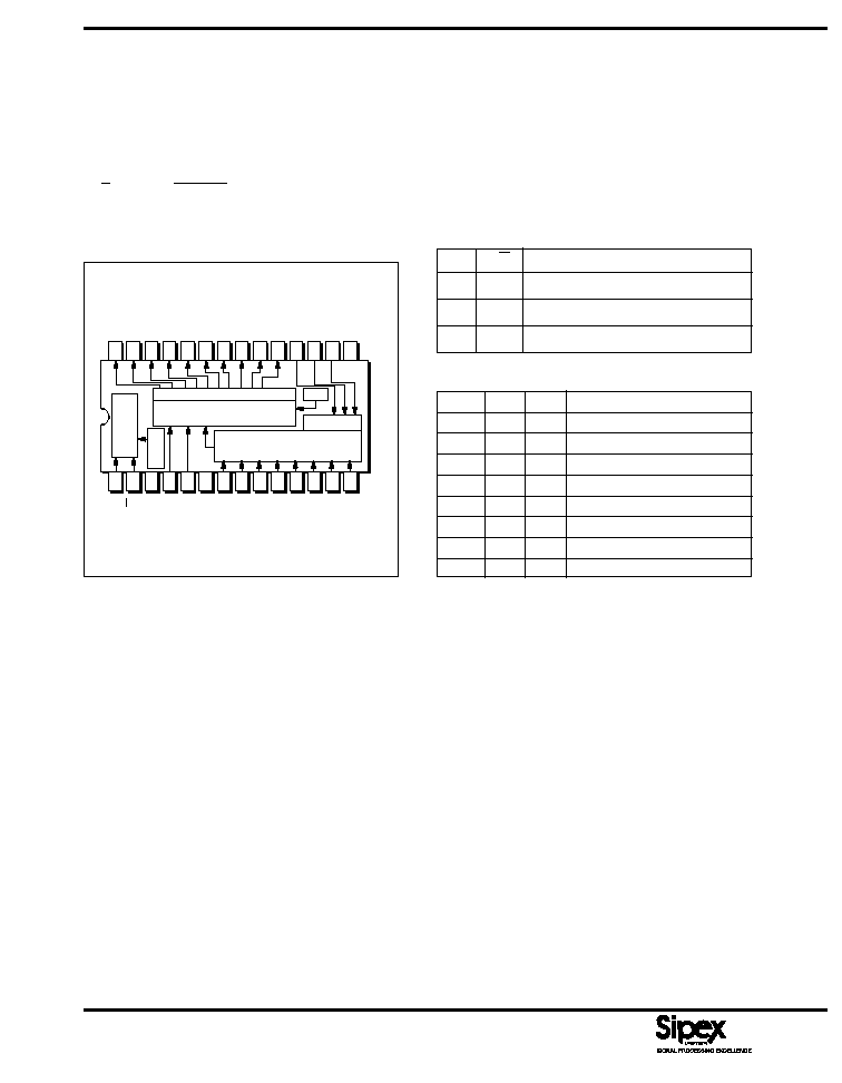
PIN FUNCTION...
A
0
-- Device Address -- Logic low enables 8
MSB read; logic high enables 4 LSB read
STATUS -- Identifies valid data output; goes to
logic high during conversion; goes to logic low
when conversion is completed and data is valid
R/C -- Read/Convert -- Initiates conversion on
the high-to-low transition; logic low disconnects
data bus; logic high initiates read
CE -- Chip Enable -- Logic low disables read
or convert; logic high enables read or convert
MA
0
, MA
1
, MA
2
-- MUX Address 0, 1 & 2 --
Selects analog input channels CH
0
through CH
7
DB
0
through DB
11
-- Data Outputs -- Logic
high is binary true; logic low binary false
1
16
2
3
4
5
6
7
8
9 10 11 12 13 14
15
17
23 22 21 20 19 18
24
28 27 26 25
STATUS
DB11/DB3
DB10/DB2
DB9/DB1
DB8/DB0 (LSB)
DB7
DB6
DB5
DB4
MA2
MA1
MA0
DIG. GND.
V
LOGIC
A
0
R/C
V
CC
OFFSET ADJ.
GAIN ADJ.
ANA. GND.
ANA. IN. CH0
ANA. IN. CH1
ANA. IN. CH2
ANA. IN. CH3
ANA. IN. CH4
ANA. IN. CH5
ANA. IN. CH6
ANA. IN. CH7
CONTROL
LOGIC
CLOCK
12-BIT ADC
8-CHANNEL
MULTIPLEXER
DECODE
REF
MULTIPLEXER TRUTH TABLE
MA
2
MA
1
MA
0
OPERATION
0
0
0
CH
O
Selected
0
0
1
CH
1
Selected
0
1
0
CH
2
Selected
0
1
1
CH
3
Selected
1
0
0
CH
4
Selected
1
0
1
CH
5
Selected
1
1
0
CH
6
Selected
1
1
1
CH
7
Selected
CONTROL TRUTH TABLE
A
O
R/C
OPERATION
X
H ->L
Start Conversion
0
1
Enable 8 MSBs
1
1
Enable 4 LSBs

293
FEATURES...
The SP8480 Series are complete data acquisi-
tion systems, featuring 8-channel multiplexer,
internal reference and 12-bit sampling A/D con-
verter implemented as a single monolithic IC.
The analog multiplexer accepts 0V to +5V uni-
polar full scale inputs. Output data is formatted
as an 8-bit/4-bit nibble.
Linearity errors of
±
0.5 and
±
1.0 LSB, and
Differential Non-linearity to 12-bits is guaran-
teed, with no missing codes over temperature.
Channel-to-channel crosstalk is typically -85dB.
Multiplexer settling plus acquisition time is 1.9
µ
s
maximum; A/D conversion time is 8.1
µ
s maxi-
mum.
Versions of the SP8480 are available in 28-pin
plastic DIP, ceramic DIP or SOIC packages.
Operating temperature ranges are 0
°
C to +70
°
C
commercial and -40
°
C to +85
°
C industrial.
The SAR, timed by the clock, sequences through
the conversion cycle and returns an endof
convert flag to the control section of the ADC.
The clock is then disabled by the control section,
which puts the STATUS output line low. The
control section is enabled to allow the data to be
read by external command (R/C).
Multiplexer Control and Inputs
On the SP8480 the multiplexer is independent
of any other control line. The address line latches
MA
0
, MA
1
and MA
2
are hard-wired in an enabled
mode in the SP8480, and are therefore transpar-
ent. Data setup time for these inputs is 50ns. If
a device is required with additional MUX con-
trol, please refer to the Sipex SP8481 DAS.
Since the latches are enabled, MUX channel
select data need not be held by the bus for a
minimum period of 3.0
µ
s after the conversion
has been initiated. This is the time required for
the MUX and Sample and Hold to settle. How-
ever it is advisable that the MUX not be changed
at all during the full 10
µ
s conversion time due to
capacitive coupling effects of digital edges
through the silicon.
The SP8480 multiplexer inputs have been de-
signed to allow substantial overvoltage condi-
tions to occur without any damage. The inputs
are diode-clamped and further protected with a
200
series resistor. As a result, momentary (10
seconds) input voltages can be as low as -16.5V
or as high as +31.5V with no change or degrada-
tion in multiplexer performance or crosstalk.
This feature allows the output voltage of an
externally connected op amp to swing to
±
15V
supply levels with no multiplexer damage. Com-
plicated power-up sequencing is not required to
protect the SP8480. The multiplexer inputs may
be damaged, however, if the inputs are allowed
to either source or sink greater than 100mA.
Initiating A Conversion
Please refer to Figure 4. The SP8480 was de-
signed to require a minimum of control to per-
form a 12-bit conversion. The control input used
is R/C which tri-states the outputs and starts the
conversion when low. The STATUS line indi-
cates when a conversion is in process and when
it is complete. The A
0
control input is used to
CIRCUIT OPERATION...
The SP8480 is a complete 8-channel data acqui-
sition systems (DAS), with on-board multi-
plexer, voltage reference, sample-and-hold, clock
and tri-state outputs. The digital control archi-
tecture is very similar to the industry-standard
574-type A/D, and uses identical control lines
and digital states.
The multiplexer for the SP8480 is identical in
operation to many discrete devices available
today, except that it has been integrated into the
single-chip DAS. The appropriate channel is
selected using the MUX address lines MA
0
,
MA
1
, and MA
2
per the truth table. The selected
analog input is fed through to the ADC. The
input impedance into any MUX channel will be
on the order to 10
9
ohms, since it is connected to
the integral sampling structure of the capacitor
DAC. Crosstalk is kept to -85dB at 0V to 5V
p-p
over an input frequency range of 10kHz to 50kHz.
When the internal control section of the SP8480
initiates a conversion command the internal clock
is enabled, and the successive approximation
register (SAR) is reset to all zeros. Once the
conversion has been started it cannot be stopped
or restarted. Data is not available at the output
buffers until the conversion has been completed.
294
latch the 8 MSB's and 4 LSB's of output data on
the 8-bit wide output data bus.
The conversion cycle is started when R/C is
brought low and must be held low for a mini-
mum of 50ns. The R/C signal will also cause the
output latches to be in a tri-state mode when low.
Approximately 200ns after R/C is low, STA-
TUS will change from low to high. This output
signal will stay high while the SP8480 is per-
forming a conversion. Valid data will be latched
to the output bus, through internal control, 500ns
prior to the STATUS line transitioning from a
high to low.
Reading the Data
Please refer to Figure 5. To read data from the
SP8480, the R/C and A
0
control lines are used.
R/C must be high a minimum of 50ns prior to
reading the data to allow time for the output
latches to come out of the high impedance tri-state
mode. A
0
is used to access the data. The first 8
MSBs will be on pins 26 through 19, with pin 26
being the MSB. The remaining 4 LSBs will be on
pins 23 through 26 with pin 23 being the LSB.
When A
0
is switched from one state to the next,
there is a 50ns output latch propagation delay
between the MSBs and LSBs being present on
the output pins.
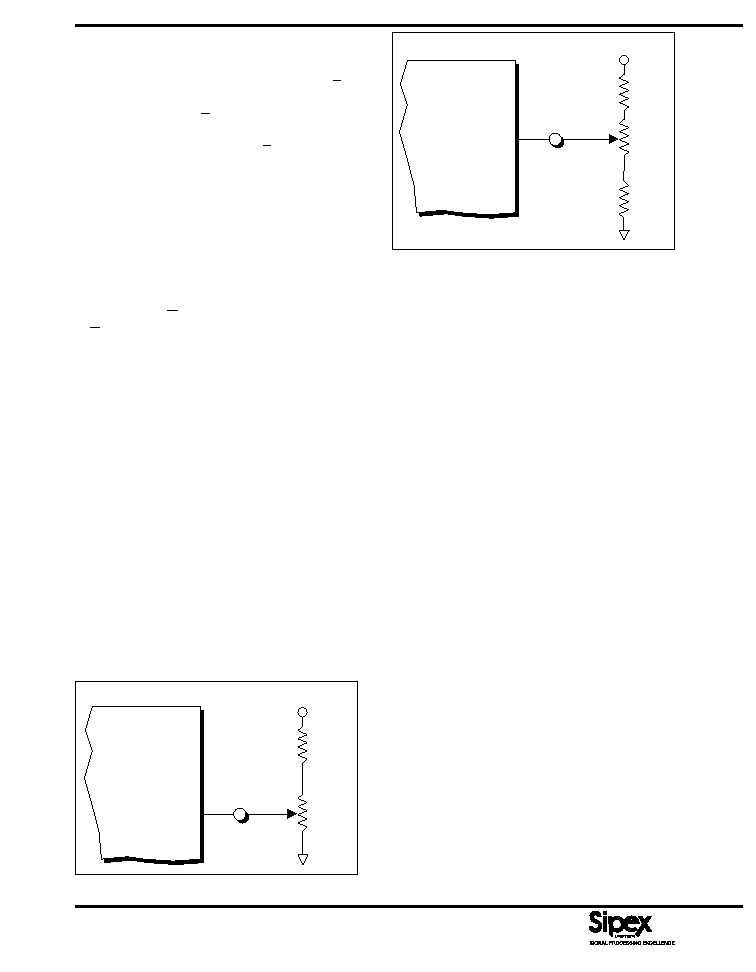
CALIBRATION
The calibration procedure for the SP8480 con-
sists of adjusting the most negative input voltage
(0V) to the ideal output code for offset adjust-
ment, and then adjusting the most positive input
voltage (5.0V) to its ideal output code for gain
adjustment.
SP8480
GAIN ADJUST
125K
+15V
10K
±0.3% Trim Range
5
19K
Center pot
for zero
correction
Figure 2. Gain Adjust
Offset Adjustment
The offset adjustment must be completed first.
Please refer to Figure 1. Apply an input voltage
of 0.5LSB or 610
µ
V to any multiplexer input.
Adjust the offset potentiometer so that the output
code fluctuates evenly between 000...000 and
000...001. It is only necessary to observe the
lower eight LSB's during this procedure.
Gain Adjustment
With the offset adjusted, the gain error can now
be trimmed to zero (see Figure 2). The ideal
input voltage corresponding to 1.5 LSB's below
the nominal full scale input value, or +4.988V, is
applied to any multiplexer input. The gain poten-
tiometer is adjusted so that the output code
alternates evenly between 111...111 and
111...110. Again, only the lower eight LSB's
need be observed during this procedure. With the
above adjustment made, the converter is now
calibrated.
SP8480
OFFSET ADJUST
100K
+15V
5K
1.5mV to +3mV
4
Figure 1. Offset Adjust
295
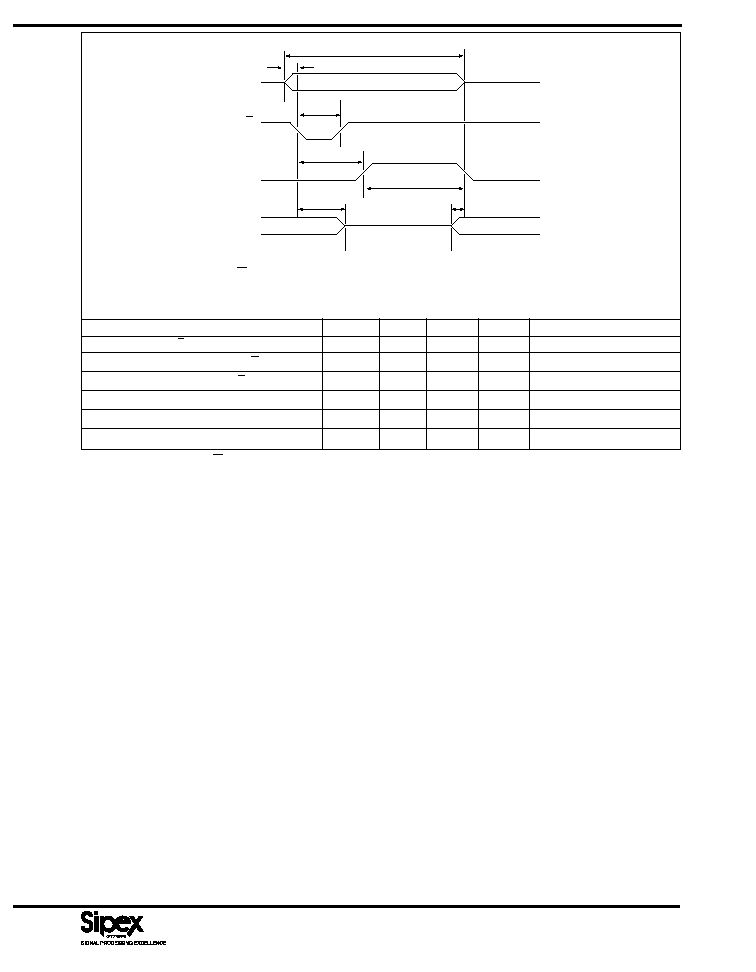
LOW PULSE FOR R/C DYNAMIC CHARACTERISTICS
V
CC
= +15V; V
LOGIC
= +5V; T
A
= 25
°
C
PARAMETER
MIN
TYP
MAX
UNIT
CONDITIONS
t
HRL
Low R/C Pulse Width
50
ns
t
DS
Status Delay from R/C
200
ns
t
HDR
Data Valid after R/C Low
25
ns
t
HS
Status Delay after Data Valid
500
ns
t
MDS
MUX Data Setup
50
ns
t
MDH
MUX Data Valid
3
10
µ
s
Figure 3. Low Pulse for R/C Timing
R/C
STATUS
DB
11
- DB
0
t
HRL
t
C
DATA VALID
DATA VALID
t
MDH
t
DS
t
HDR
t
HS
MA
0
- MA
2
t
MDS
296
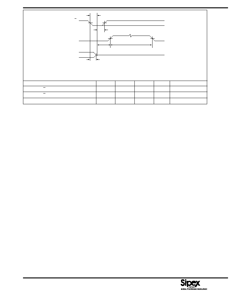
CONVERT MODE DYNAMIC CHARACTERISTICS
V
CC
= +15V; V
LOGIC
= +5V; T
A
= 25
°
C
PARAMETER
MIN
TYP
MAX
UNIT
CONDITIONS
t
SRC
R/C to CE Setup
50
ns
t
HRC
R/C Low during CE High
50
ns
t
DSC
Status Delay from CE
200
ns
Figure 4. Convert Mode Timing
R/C
STATUS
DB
11
- DB
0
t
C
t
SRC
HIGH IMPEDANCE
t
HRC
t
DSC
t
HDR
297
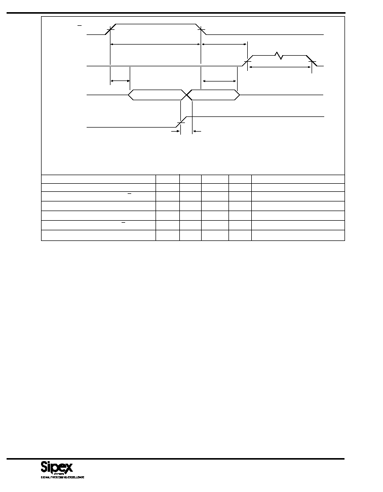
R/C
STATUS
DB
11
- DB
0
t
HRH
t
C
DATA VALID
t
HDR
t
DDR
t
DS
HIGH
IMPEDANCE
DATA VALID
DB11DB4
DB3DB0, 0000
A
0
t
ADS
HIGH
IMPEDANCE
Figure 5. Read Mode Timing
READ MODE DYNAMIC CHARACTERISTICS
V
CC
= +15V; V
LOGIC
= +5V; T
A
= 25
°
C
PARAMETER
MIN
TYP
MAX
UNIT
CONDITIONS
t
HRH
Read Pulse Width
150
ns
t
DS
Status Delay from R/C
200
ns
t
C
Conversion Time
10
µ
s
t
DDR
Data Bits Out of High Z Delay
0
100
ns
t
HDR
Data Valid after R/C Low
25
ns
t
ADS
A
0
High or Low to Data Setup
50
ns
298
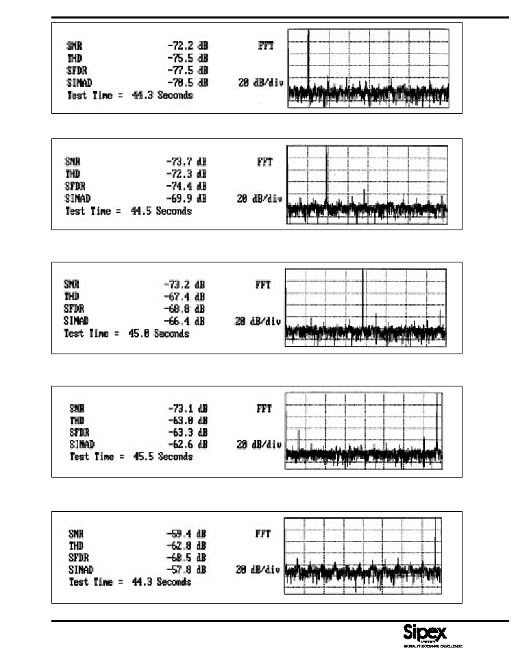
Figure 6. FFT; 6kHz 5V (0dB) Full Scale Input; F
S
=10kHz
Figure 10. FFT; 48kHz 1V (14dB) Input; F
S
=10kHz
Figure 7. FFT; 12kHz 5V (0dB) Full Scale Input; F
S
=10kHz
Figure 8. FFT; 24kHz 5V (0dB) Full Scale Input; F
S
=10kHz
Figure 9. FFT; 48kHz 5V (0dB) Full Scale Input; F
S
=10kHz

299
ORDERING INFORMATION
12-Bit Data Acquisition System with 12-Bit Parallel Data Output:
Commercial (0
°
C to +70
°
C):
NonLinearity
Package
SP8480JP ....................................................................................
±
1.0LSB INL ................................................................... 28pin, 0.6" Plastic DIP
SP8480KP ...................................................................................
±
0.5LSB INL ................................................................... 28pin, 0.6" Plastic DIP
SP8480JS ....................................................................................
±
1.0LSB INL ............................................................................ 28pin, 0.3" SOIC
SP8480KS ...................................................................................
±
0.5LSB INL ............................................................................ 28pin, 0.3" SOIC
Industrial (-40
°
C to +85
°
C):
NonLinearity
Package
SP8480AP ...................................................................................
±
1.0LSB INL ................................................................... 28pin, 0.6" Plastic DIP
SP8480BP ...................................................................................
±
0.5LSB INL ................................................................... 28pin, 0.6" Plastic DIP
SP8480AS ...................................................................................
±
1.0LSB INL ............................................................................ 28pin, 0.3" SOIC
SP8480BS ...................................................................................
±
0.5LSB INL ............................................................................ 28pin, 0.3" SOIC

300
THIS PAGE LEFT INTENTIONALLY BLANK