 | –≠–ª–µ–∫—Ç—Ä–æ–Ω–Ω—ã–π –∫–æ–º–ø–æ–Ω–µ–Ω—Ç: SP8531JS | –°–∫–∞—á–∞—Ç—å:  PDF PDF  ZIP ZIP |
SP8531DS/01 SP8531 12-Bit Sampling Serial Out Analog to Digital Converter
© Copyright 1999 Sipex Corporation
1
s
12 Bit Resolution
s
Single +5Volt Supply
s
Internal Reference, 1.25V
s
Unipolar 0 to +2.5 Volt Input Range
s
Fast, 3.75
µ
s Conversion Time
s
Fast Power Shutdown/Turn-On Mode
s
3-Wire Synchronous Serial High Speed
Interface
s
2
µ
A Shutdown Mode (10
µ
W)
s
Low Power CMOS 60mW typical
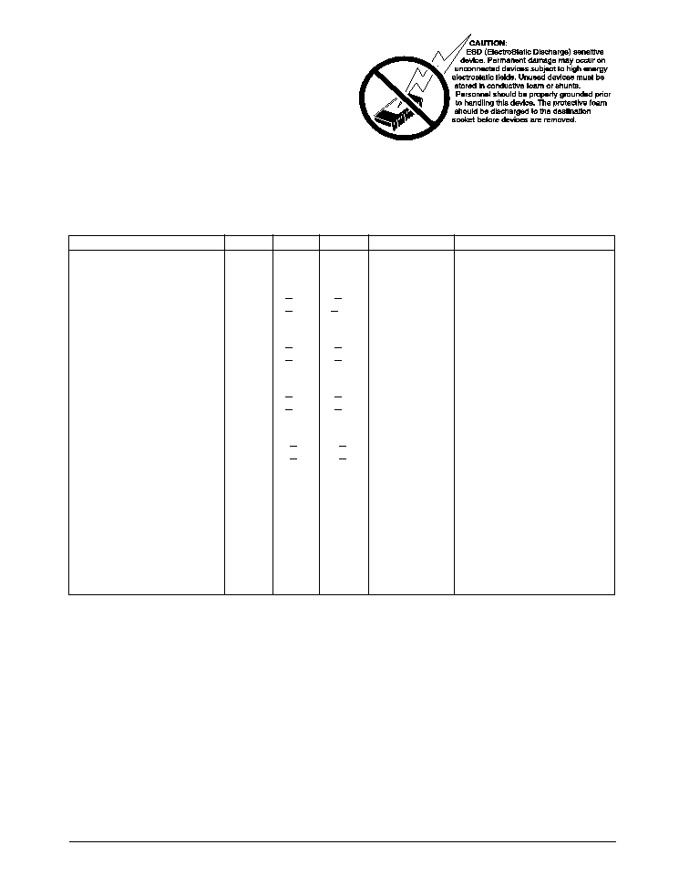
SP8531
12-Bit Sampling Serial Out Analog
to Digital Converter
DESCRIPTION
The SP8531 is a sampling 12-Bit serial out analog to digital converter. The device contains a high
speed 12-Bit analog to digital converter, internal reference, and sample/hold circuitry. The
SP8531 is available in 16-pin PDIP and SOIC packages, specified over Commercial and
Industrial temperature ranges.
CONTROL
LOGIC
COUNTER
SAR
CDAC
LATCHED
COMPARATOR
BUFFER
STATUS
D
OUT
REF.
CS
SCLK
V
IN
OFFSET
ADJUST
SHUTDOWN
GAIN
ADJUST
REF OUT
RTRIM
BUFFER
SIGNAL PROCESSING EXCELLENCE
SP8531DS/01 SP8531 12-Bit Sampling Serial Out Analog to Digital Converter
© Copyright 1999 Sipex Corporation
2
ABSOLUTE MAXIMUM RATINGS
(TA=+25∞C unless otherwise noted) ..............................................
VDD to DGND ............................................................. -0.3V to +7V
VDA to AGND .............................................................. -0.3V to +7V
Vin to AGND .................................................... -0.3V to VDA +0.3V
Digital Input to VSS ........................................... -0.3V to VDD+0.3V
Digital Output to VSS ........................................ -0.3V to VDD+0.3V
Operating Temp. Range
Commercial (J,K Version) ............................... 0∞C to 70∞C
Industrial (A,B Version) .............................. -40∞C to +85∞C
Storage Temperature ............................................... -65∞C to 150∞C
Lead Temperature(Solder 10 sec) ....................................... +300∞C
Power Dissipation to +70∞C ................................................ 500mW
Derate Above 70∞C ......................................................... 10mW/ ∞C
SPECIFICATIONS
Unless otherwise noted the following specifications apply for V
DD
= 5V with limits applicable for T
A
= 25∞C.
PARAMETER
MIN.
TYP.
MAX.
UNIT
CONDITIONS
DC Accuracy
Resolution
12
Bits
Integral Linearity
J, A
+0.6
+1.0
LSB
K ,B
+0.4
+0.75
LSB
Differential Linearity Error
J, A
+0.5
+1.0
LSB
No Missing Codes
K ,B
+0.5
+1.0
LSB
No Missing Codes
Gain Error
J, A
+0.2
+1.0
%FSR
Externally Trimmable to Zero
K,B
+0.1
+0.5
%FSR
Externally Trimmable to Zero
Offset Error
J, A
+4
+7
LSB
Externally Trimmable to Zero
K,B
+3
+5
LSB
Externally Trimmable to Zero
Analog Input
0 to 2.5
Volts
Input Impedance
600K
Ohms
4 MHz Clock Rate
Conversion Speed
Sample Time
400
ns
Conversion Time
3.75
µ
s
Complete Cycle
4.25
µ
s
Conversion
Rate:
235
KHz
Clock Speed
4
MHz
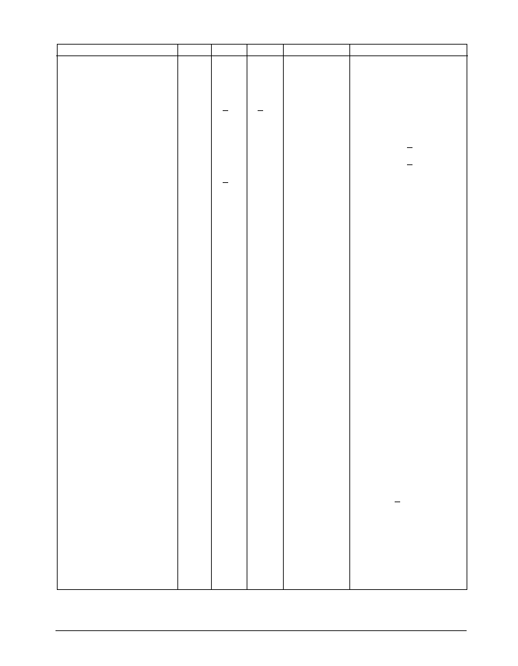
SP8531DS/01 SP8531 12-Bit Sampling Serial Out Analog to Digital Converter
© Copyright 1999 Sipex Corporation
3
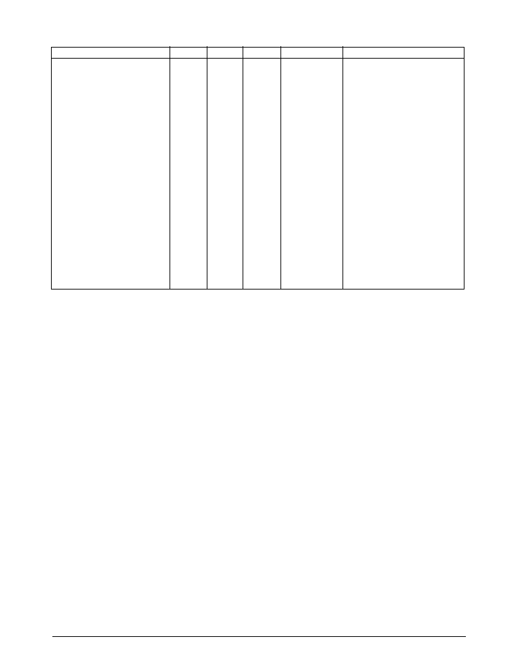
SPECIFICATIONS
(continued)
Unless otherwise noted the following specifications apply for V
DD
= 5V with limits applicable for T
A
= 25∞C.
PARAMETER
MIN.
TYP.
MAX.
UNIT
CONDITIONS
Reference Output
1.25
Volts
Ref. Out Temp. Coef.
J, A
30
ppm/∞C
K,B
20
ppm/∞C
Ref.Out Error
+4
+25
mV
Output Current
1
mA
Digital Inputs
Input Low Voltage , VIL
0.8
Volt
VDD
=
5V +5%
Input High Voltage , VIH
2.0
Volt
VDD
=
5V +5%
Input Current IIN
+1
µ
A
Input Capacitance
3
pF
Digital Outputs
Data Format (1)
Data Coding (2)
VOH
4.0
Volt VDD=5V
±
5%, IOH=-0.4mA
VOL
0.4
Volt VDD=5V
±
5%, IOL=+1.6mA
AC Accuracy
fin=47KHz,VDD=5.0V
@ 25∞C, SCLK=4MHz
Spurious Free Dynamic
Range (SFDR)
83
dB
Total Harmonic Distortion
(THD)
-80
dB
Signal to Noise &
Distortion (SINAD)
71
dB
Signal to Noise (SNR)
72
dB
Sampling Dynamics
Acquisition Time to 0.01%
200
ns
For a +FS step change
at input
-3dB Small Signal BW
13
MHz
Aperture Delay
35
ns
Aperture Jitter
10
ps RMS
SP8531DS/01 SP8531 12-Bit Sampling Serial Out Analog to Digital Converter
© Copyright 1999 Sipex Corporation
4
SPECIFICATIONS
(continued)
Unless otherwise noted the following specifications apply for V
DD
= 5V with limits applicable for T
A
= 25∞C.
PARAMETER
MIN.
TYP.
MAX.
UNIT
CONDITIONS
Power Supplies
VDD
4.75
5.25
Volts
Supply Current
Operating Mode
11.5
17
mA
SD=0, VDD=+5.0V
Shutdown Mode
0.01
2
µ
A
SD=1, V
DD
= +5.0V
Power Dissipation
Operating Mode
60
85
mW
SD=0
Shutdown Mode
0.05
10
µ
W
SD=1
Power Turn On
20
µ
S
Via Shutdown Control
to 1 LSB settling error.
Temperature Range
Commercial
0
to
+70
∞C
Industrial
-40
to
+85
∞C
Storage
-65
to
+150
∞C
(1) Data Format is 12-Bit Serial
(2) Data Coding is Binary (See Timing Diagram)
SP8531DS/01 SP8531 12-Bit Sampling Serial Out Analog to Digital Converter
© Copyright 1999 Sipex Corporation
5
CIRCUIT OPERATION
Figure 1 shows a simple circuit required to
operate the SP8531. The conversion is
controlled by the user supplied signal Chip
Select Bar (CS) which selects and deselects the
device, and a system clock (SCLK).
A high level applied to CS asynchronously
clears the internal logic, puts the sample & hold
(CDAC) into sample mode and places the DOUT
(Data Output) pin in a high impedance state.
Conversion is initiated by falling edge on CS in
slave mode at which point the input voltage is
held and a conversion is started. A delay of 90ns
is required between the falling edge of CS and
the first rising of SCLK.
The device responds to the shut down signal
asynchronously so that a conversion in progress
will be interrupted and the resulting data will
be erroneous. A 20
µ
Sec minimum delay is
required between the falling edge of shut down
and initiation of a conversion.
Data Format
16 bits of data are sent for each conversion. The
data is shipped with 4 leading "0"s, and then 12
bits of data, MSB first. Data changes on the
falling edge of SCLK and is stable on the rising
edge of SCLK.
Continuous stand alone operation is obtained by
holding CS low. In this mode an oscillator is
connected directly to the SCLK pin. The SCLK
signal along with the STATUS output Signal
are used to synchronize the host system with the
converter's data. In this mode there is a single
dead SCLK cycle between the 16th clock of one
conversion and the first clock of the following
conversion for the SP8531. At a clock
frequency of 4 MHz the SP8531 provides a
throughput rate of 235KHz.
In slave mode operation, CS is brought high
between each conversion so that all conversions
are initiated by falling edge on CS.
FEATURES
The SP8531 is a sampling, 12-Bit serial out
data acquisition system. The device contains a
high speed 12-bit analog to digital converter,
internal reference, and sample and hold
circuitry.
The SP8531 is fabricated in Sipex' Bipolar
Enhanced CMOS Process that permits state-of-
the-art design using bipolar devices in the
analog/linear section and extremely low power
CMOS in the digital/logic section.
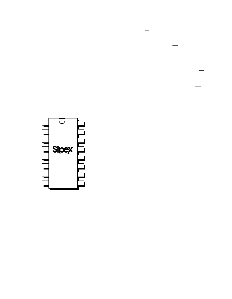
PIN ASSIGNMENTS
Pin 1-N.C.-No Connection
Pin 2-N.C.-No Connection
Pin 3-VIN - Analog Input
Pin 4-AGND-Analog Ground
Pin 5-VSS-Digital Ground
Pin 6-SCLK-Serial Clock Input
Pin 7-DOUT Digital Data Output
Pin 8-STATUS- High During Conversion
Pin 9-CS-Chip Select Bar Input -
High Deselects chip -Low Selects chip
Pin 10-SD-Shutdown Input, logic low=power
up, logic high = powerdown
Pin 11-VDD Digital +5V supply
Pin 12-VDA Analog +5V supply
Pin 13-OffADJ- External Offset Adjust
Pin 14-N.C.-No Connection
Pin 15-REFOUT-Voltage Reference Output
Pin 16-GAINADJ-External Gain Adjustment
16
15
14
13
12
11
10
9
GAIN ADJUST
REF OUT
N.C.
OFFSET ADJ.
V
DA
V
DD
SD
CS
1
2
3
4
5
6
7
8
N.C.
N.C.
V
IN
AGND
V
SS
SCLK
D
OUT
STATUS
SP8531