 | ÐлекÑÑоннÑй компоненÑ: SP8544KN | СкаÑаÑÑ:  PDF PDF  ZIP ZIP |
Äîêóìåíòàöèÿ è îïèñàíèÿ www.docs.chipfind.ru
SP8542/8544DS/01 SP8542/8544 Two and Four Channel 12-Bit Multiplexed Sampling ADC's
© Copyright 2000 Sipex Corporation
1
SP8542/SP8544
s
Two or Four Channel Input Mux
s
12 Bit Resolution
s
Single +5Volt Supply
s
Internal 1.25 Volt Reference
s
Unipolar 0 to +2.5 Volt Input Range
s
Fast, 3.75
µ
s Conversion Time per Channel
s
Fast Power Shutdown/Turn-On Mode
s
3-Wire Synchronous Serial High Speed
Interface
s
2
µ
A Shutdown Mode (10
µ
W)
s
Low Power CMOS 42mW typical
DESCRIPTION
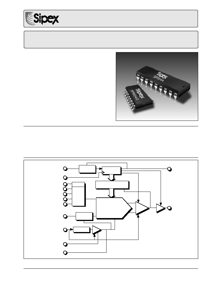
The SP8542 (2 channel) and SP8544 (4 channel) are 12-Bit serial in/out data acquisition systems
with a bi-directional serial interface. The devices contain a high speed 12-Bit analog to digital
converter, internal reference, and a 2 or 4 channel input mux which drives the internal sample/
hold circuitry. The SP8542 is available in 16-pin PDIP and SOIC packages, and the SP8544
is available in 18-pin PDIP and SOIC packages, specified over Commercial and Industrial
temperature ranges.
Two and Four Channel 12-Bit Multiplexed
Sampling ADCs
CONTROL
LOGIC
COUNTER
SAR
CDAC
LATCHED
COMPARATOR
BUFFER
STATUS
D
OUT
REF.
CS
SCLK
*CH3
OFFSET
ADJUST
SHUTDOWN
GAIN
ADJUST
REF OUT
RTRIM
*CH2
CH1
CH0
DIN
MUX
MUX
Register
SP8542 - 2 CHANNEL MUX
*SP8544 - 4 CHANNEL MUX
®
SP8542/8544DS/01 SP8542/8544 Two and Four Channel 12-Bit Multiplexed Sampling ADC's
© Copyright 2000 Sipex Corporation
2
SPECIFICATIONS
Unless otherwise noted the following specifications apply for V
DD
= 5V with limits applicable for T
A
= 25°C.
PARAMETER
MIN.
TYP.
MAX.
UNIT
CONDITIONS
DC Accuracy
Resolution
12
Bits
Integral Linearity
J, A
+0.6
+1.0
LSB
K ,B
+0.4
+0.75
LSB
Differential Linearity Error
J, A
+0.5
+1.0
LSB
No Missing Codes
K ,B
+0.5
+1.0
LSB
No Missing Codes
Gain Error
J, A
+0.2
+1.0
%FSR
Externally Trimmable to Zero
K,B
+0.1
+0.5
%FSR
Externally Trimmable to Zero
Offset Error
J, A
+4
+7
LSB
Externally Trimmable to Zero
K,B
+3
+5
LSB
Externally Trimmable to Zero
Analog Input
0 to 2.5
Volts
Input Impedance
On Channel
8
pF
In series with 1.4K
Off Channel (2)
1.0
G
note 2
Input Bias Current
1.0
nA
Channel to Channel
Crosstalk
Off to On Channel
-90
-80
dB
@ 10KHz Full Scale sine wave
Conversion Speed
Sample Time (1)
400
ns
Conversion Time (1)
3.75
µ
s
Complete Cycle (1)
4.25
µ
s
Convert Rate (1)
117.6
KHz
2 Channels
Clock Speed
4
MHz
Date Rate (1)
235
KHz
Total Conversion Rate
Convert Rate (1)
58.8
KHz
4 Channels
ABSOLUTE MAXIMUM RATINGS
(TA=+25°C unless otherwise noted) ..............................................
VDD to DGND ............................................................. -0.3V to +7V
VDA to AGND .............................................................. -0.3V to +7V
Vin to AGND .................................................... -0.3V to VDA +0.3V
Digital Input to VSS ........................................... -0.3V to VDD+0.3V
Digital Output to VSS ........................................ -0.3V to VDD+0.3V
Operating Temp. Range
Commercial (J,K Version) ............................... 0°C to 70°C
Industrial (A,B Version) ............................. -40°C to +85°C
Storage Temperature ............................................... -65°C to 150°C
Lead Temperature(Solder 10sec) ...................................... +300°C
Power Dissipation to +70°C ............................................... 500mW
Derate Power Dissipation Above 70°C ......................... 10mW/ °C
SP8542/8544DS/01 SP8542/8544 Two and Four Channel 12-Bit Multiplexed Sampling ADC's
© Copyright 2000 Sipex Corporation
3
SPECIFICATIONS
(continued)
Unless otherwise noted the following specifications apply for V
DD
= 5V with limits applicable for T
A
= 25°C.
PARAMETER
MIN.
TYP.
MAX.
UNIT
CONDITIONS
Reference Output
1.25
Volt
Ref. Out Temp. Coef.
J, A
30
ppm/°C
K,B
20
ppm/°C
Ref.Out Error
+4
+25
mV
Output Current
1
mA
Digital Inputs
Input Low Voltage , VIL
0.8
Volt
VDD
=
5V
±
5%
Input High Voltage , VIH
2.0
Volt
VDD
=
5V
±
5%
Input Current IIN
+1
µ
A
Input Capacitance
3
pF
Digital Outputs
Data Format (3)
Data Coding (4)
VOH
4.0
Volt
VDD=5V
±
5%, IOH=-0.4mA
VOL
0.4
Volt
VDD=5V
±
5%, IOL=+1.6mA
AC Accuracy
Spurious Free Dynamic
78
dB
fin=47KHz
Range (SFDR)
Total Harmonic Distortion
(THD)
-74
dB
fin=47KHz
Signal to Noise &
Distortion (SINAD)
70
dB
fin=47KHz
Signal to Noise (SNR)
71
dB
fin=47KHz
Sampling Dynamics
Acquisition Time to 0.01%
250
ns
-3dB Small Signal BW
13
MHz
Aperture Delay
35
ns
Aperture Jitter
10
ps RMS
SP8542/8544DS/01 SP8542/8544 Two and Four Channel 12-Bit Multiplexed Sampling ADC's
© Copyright 2000 Sipex Corporation
4
SPECIFICATIONS
(continued)
Unless otherwise noted the following specifications apply for V
DD
= 5V with limits applicable for T
A
= 25°C.
PARAMETER
MIN.
TYP.
MAX.
UNIT
CONDITIONS
Power Supplies
VDD
+4.75
+5
+5.25
V
Supply Current
Operating Mode
8.4
14
mA
SD=0
Shutdown Mode
.01
2
µ
A
SD=1
Power Dissipation
Operating Mode
42
70
mW
SD=0
Shutdown Mode
0.05
10
µ
W
SD=1
Power Turn On
20
µ
S
Via Shutdown Control
to 1 LSB settling error.
Temperature Range
Commercial
0
to
+70
°C
Industrial
-40
to
+85
°C
Storage
-65
to
+150
°C
(1) Free Running Mode
(2) Note that the transition from off to on causes charging currents that increase
the average input current
(3) Data Format is 12-Bit Serial
(4) Data Coding is binary (see Timing Diagram)
SP8542/8544DS/01 SP8542/8544 Two and Four Channel 12-Bit Multiplexed Sampling ADC's
© Copyright 2000 Sipex Corporation
5
SP8542 PIN ASSIGNMENTS
Pin 1-N.C.-No Connection
Pin 2-CH0-Analog Mux Input 0
Pin 3-CH1-Analog Mux Input 1
Pin 4-AGND-Analog Ground
Pin 5-VSS Digital Ground
Pin 6-SCLK-Serial Clock Input
Pin 7-DOUT Digital Data Output
Pin 8-DIN Mux Channel Selection Input
Pin 9-Status
Pin 10-CS-Chip Select Bar Input, High
Deselects chip, Low Selects chip
Pin 11-SD-Shutdown Input, logic low = power
up, logic high = powerdown
Pin 12-VDD Digital +5V supply
Pin 13-VDA Analog +5V supply
Pin 14-OffADJ External Offset Adjust
Pin 15-Refout-Voltage Reference Output
Pin 16-GAINADJ-External Gain Adjustment
GAIN ADJUST
REF OUT
OFFSET ADJ.
V
DA
V
DD
SD
CS
STATUS
1
2
3
4
5
6
7
8
N.C.
CH0
CH1
AGND
V
SS
SCLK
D
OUT
DIN
16
15
14
13
12
11
10
9
SP8542
SP8544 PIN ASSIGNMENTS
Pin 1-N.C.-No Connection
Pin 2-CH0-Analog Mux Input 0
Pin 3-CH1-Analog Mux Input 1
Pin 4-CH2-Analog Mux Input 2
Pin 5-CH3-Analog Mux Input 3
Pin 6-AGND-Analog Ground
Pin 7-VSS Digital Ground
Pin 8-SCLK-Serial Clock Input
Pin 9-DOUT Digital Data Output
Pin 10-DIN Mux Channel Selection Input
Pin 11-Status
Pin 12-CS-Chip Select Bar Input, High
Deselects chip, Low Selects chip
Pin 13-SD-Shutdown Input, logic low = power
up, logic high = powerdown
Pin 14-VDD Digital +5V supply
Pin 15-VDA Analog +5V supply
Pin 16-OffADJ External Offset Adjust
Pin 17-Refout-Voltage Reference Output
Pin 18-GAINADJ-External Gain Adjustment
GAIN ADJUST
REF OUT
OFFSET ADJ.
V
DA
V
DD
SD
CS
STATUS
DIN
1
2
3
4
5
6
7
8
N.C.
CH0
CH1
CH2
CH3
AGND
V
SS
SCLK
D
OUT
9
18
17
16
15
14
13
12
11
10
SP8544
SP 8542 Channel Selection
Truth Table
MA0
Channel Selection
0
CH0
1
CH1
SP 8544 Channel Selection
Truth Table
MA1
MA0
Channel Selection
0
0
CH0
0
1
CH1
1
0
CH2
1
1
CH3
SP8542/8544DS/01 SP8542/8544 Two and Four Channel 12-Bit Multiplexed Sampling ADC's
© Copyright 2000 Sipex Corporation
6
1
GAIN ADJUST
N.C.
2
REF OUT
CH0
4
5
OFFSET ADJ.
6
V
DA
V
SS
7
V
DD
SCLK
8
CS
D
OUT
9
STATUS
SP8542
STATUS OUT
DATA OUT
CLOCK IN
10kOhms
0.01
µ
F*
* Optional filter capacitor is helpful in a noisy pc board application.
3
CH1
AGND
SD
DIN
DATA IN
CHIP SELECT
CH1
CH0
+5V
0.1
µ
F
0.1
µ
F
6.8
µ
F
SHUT DOWN
2kOhms
5kOhms
+
15
14
13
12
11
10
16
Figure 1. Operating Circuit
FEATURES
The SP8542 and SP8544 are two and four
channel 12-Bit serial In/Out data acquisition
system. The device contains a high speed 12-bit
analog to digital converter, internal reference,
and a two or four channel input Mux which
drives the internal sample and hold circuit.
The SP8542 and SP8544 are fabricated in Sipex'
Bipolar Enhanced CMOS Process that permits
state-of-the-art design using bipolar devices in
the analog/linear section and extremely low
power CMOS in digital/logic section.
CIRCUIT OPERATION
Figure 1 and 2 shows a simple circuit required to
operate the SP8542 and SP8544. Please refer to
the free running mode timing diagram or the
slave mode timing diagram. The conversion is
controlled by the user supplied signals Chip
Select Bar (CS) which selects and deselects the
device, and a system clock (SCLK).
A high level applied to CS asynchronously
clears the internal logic, puts the sample & hold
(CDAC) into sample mode and places the DOUT
(Data Output) pin in a high impedance state.
Conversion is initiated by falling edge on CS in
slave mode at which point the selected input
voltage is held and a conversion is started. A
delay tCS of 90ns is required between the falling
edge of CS and the first rising of SCLK.
The device responds to the shut down signal
asynchronously so that a conversion in progress
will be interrupted and the resulting data will be
erroneous. A 20
µ
Sec delay is required between
the falling edge of shutdown and initiation of
a conversion.
Input Data Format
The SP8542 requires, in addition to the Chip
Select Bar (CS) and System Clock (SCLK)
signals, one multiplexer configuration bit
(MA0). The SP8544 requires, in addition to the
Chip Select Bar (CS) and System Clock (SCLK)
signals, two multiplexer configuration bits (MA1
and MA0). These bits are shifted into the DIN
pin, MSB first, during the first two clocks of the
16 clock conversion cycle and configure the
input multiplexer to select the desired input
channel.
SP8542/8544DS/01 SP8542/8544 Two and Four Channel 12-Bit Multiplexed Sampling ADC's
© Copyright 2000 Sipex Corporation
7
1
18
GAIN ADJUST
N.C.
2
17
REF OUT
CH0
4
15
5
14
OFFSET ADJ.
CH3
6
13
V
DA
V
SS
7
12
V
DD
SCLK
8
11
CS
D
OUT
9
10
STATUS
SP8544
CH2
STATUS OUT
DATA OUT
CLOCK IN
10kOhms
0.01
µ
F*
* Optional filter capacitor is helpful in a noisy pc board application.
16
3
CH1
CH2
AGND
SD
DIN
DATA IN
CHIP SELECT
CH3
CH1
CH0
+5V
0.1
µ
F
0.1
µ
F
6.8
µ
F
SHUT DOWN
2kOhms
5kOhms
+
Figure 2. Operating Circuit
These bits, if shifted in during the nth conversion,
will determine the input configuation for the
(n+1) conversion (see timing diagram). The
input range is 0 to 2.5V. The serial output is
Hi-Z unless conversion data is being shifted out.
It is therefore possible to tie the DIN pin to the
DOUT pin for a 3-wire interface or leave them
seperate for a 4-wire interface. The output is
compatible with SPI, QSPI and MICROWIRE
serial communication protocols.
0utput Data Format
12 Bits of data are sent in 16 clock cycles for
each conversion. Dout is in high impedance
state during the first four clock cycles of the
conversion and sends the 12 bits of data MSB
first, in the succeeding 12 clock cycles. Output
data changes on the falling edge of SCLK and is
stable on the rising edge of SCLK.
Free Running operation is obtained by holding
CS low. In this mode an oscillator is connected
directly to SCLK pin. The SCLK signal along
with the STATUS output Signal are used to
synchronize the host system with the converter's
data. In this mode there is a single dead SCLK
cycle between the 16th clock of one conversion
and the first clock of the following conversion
for both the SP8542 and SP8544. At a clock
frequency of 4 MHz the SP8542 provides a
throughput rate of 117.6KHz for both channels
and the SP8544 provides a throughput rate of
58.8KHz for all four channels. Both devices
provide a throughput rate of 235KHz for one
channel in Free Running Mode.
In slave mode operation, CS is brought high
between each conversion so that all conversions
are initiated by falling edge on CS.
Layout Considerations
Because of the high resolution and linearity of
the SP8542 and SP8544 system design
considerations such as ground path impedance
and contact resistance become very important.
To avoid introducing distortion when driving
the analog inputs of these devices, the source
resistance must be very low, or constant with
signal level. Note that in the operating circuit

SP8542/8544DS/01 SP8542/8544 Two and Four Channel 12-Bit Multiplexed Sampling ADC's
© Copyright 2000 Sipex Corporation
8
there is no connection made between VDA and
the system power supply. This is because
the analog supply pin (VDA) is connected
internally to the digital supply pin (VDD) through
a ten ohm resistor.
This connection when combined with a parallel
combination of 6.8
µ
F tantalum and 0.1
µ
F
ceramic capacitor between VDA and analog
ground, will provide some immunity to noise
which resides on the system supply. To
maintain maximum system accuracy, the
supply connected to the VDD pin should be well
isolated from digital supplies and wide load
variations.
To limit effects of digital switching elsewherein
a system, it often makes sense to run a seperate
+5Vsupply conductor from the supply requlator
to any analog components requiring +5V
including the SP8542 and SP8544. Noise on the
power supply lines can degrade the converters
performance, especially corrupting are noise
and spikes from a switching power supply.
The ground pins (AGND and VSS) on the
SP8542 and SP8544 are separated internally
and should be connected to each other under the
converter. The use of separate Analog & Digital
ground planes is usually the best technique for
preserving dynamic performance and reducing
noise coupling into sensitive converter circuits.
Where any compromise must be made the
common return of the analog input signal should
be referenced to the AGND pin of the converter.
This prevents any voltage drops that might
occur in the power supply common returns from
appearing in series with the input signal.
Coupling between analog and digital lines should
be minimized by careful layout. For instance, if
analog and digital lines must cross they should
do so at right angles. Parallel analog and digital
lines should be separated from each other by a
trace connected to common.
If external gain and offset potentiometers are
used, the potentiometers and related resistors
should be located as close to the SP8542 and
SP8544 as possible.
Minimizing "Glitches"
Coupling of external transients into an analog to
digital converter can cause errors which are
difficult to debug. In addition to the above
discussions on layout considerations, bypassing
and grounding, there are several other useful
steps that can be taken to get the best analog
performance from a system using the SP8542 or
SP8544 converter. These potential system
problem sources are particularly important to
consider when developing a new system, and
looking for causes of errors in breadboards.
First, care should be taken to avoid transients
during critical times in the sampling and
conversion process. Since the SP8542 and
SP0544 have internal sample/hold function the
signal that puts the device into hold state (CS)
going low is critical, as it would be on any
sample/hold amplfier. The CS falling edge
should have 5 to 10 ns transition time, low jitter,
and have a minimal ringing, especially during
the first 35 ns after it falls.

SP8542/8544DS/01 SP8542/8544 Two and Four Channel 12-Bit Multiplexed Sampling ADC's
© Copyright 2000 Sipex Corporation
9
TIMING CHARACTERISTICS
(Typical @ 25
°
C with V
DD
= +5V, unless otherwise noted)
PARAMETER
MIN.
TYP.
MAX.
UNIT
COND.
Thoughput Time (tTP=tA+tC)
4.25
µ
s
Acquisition Time (tA) (2 SCLK Periods)
400
500
ns
Conversion Time (tC) (15 SCLK Periods)
3.75
µ
s
SCLKLow Pulse Width (tSKL)
110
125
ns
SCLK High Pulse Width (tSKH)
110
125
ns
SCLK Period (tSKT)
250
ns
Setup Time DIN to SCLK Rising (tDISU)
0
ns
Hold Time from SCLK Rising to DIN (tDIH).
5
ns
Buss Relinquish Time (tBR)
45
ns
Setup Time -SCLK Falling to CSN Falling (tCSSU)
10
ns
CSN Low Before SCLK Rises (tCS)
90
ns
SCLK Falling to Data Valid (tSD)
50
ns
CSN Falling to STATUS Rising (tDCS)
69
ns
SCLK 17Falling to Status Rising Free Run (tDSS)
70
ns
SCLK16 Falling to Status Falling ( tDSE)
45
ns
Delay SD Low to initiate Conversion (t
PU
)
5
µ
s
Aperture Delay Slave-Mode (tAPC)
30
ns
Aperture Delay Free-Running Mode (tAPS)
35
ns
SP8542/8544DS/01 SP8542/8544 Two and Four Channel 12-Bit Multiplexed Sampling ADC's
© Copyright 2000 Sipex C
orporation
10
1
2
3
4
5
6
15
16
SCLK
CSN
STATUS
DATA
D11 D10
DATA WORD N
D0
1
2
3
4
5
6
15
16
D11 D10
DATA WORD (N+1)
1
2
3
4
5
15
16
SCLK
CS
STATUS
DATA
MODE
SD
AQUIRE
tPU
tAPC
tDCS
tCS
tCSSU
tSKT
tSKL
tSKH
tC
tSD
D11
D10
D1
D0
CONVERT
AQUIRE
tA
tBR
tDSE
DIN
D1
D0
D1
MA0
MA0
PROGRAM BIT FOR WORD (N + 1)
PROGRAM BIT FOR WORD (N + 2)
MA0
tDIH
tDISU
HI-Z
HI-Z
Timing Diagrams
Slave Mode SP8542
SP8542/8544DS/01 SP8542/8544 Two and Four Channel 12-Bit Multiplexed Sampling ADC's
© Copyright 2000 Sipex C
orporation
11
SCLK
STATUS
DATA
MODE
AQUIRE
tAPS
tDSS
tSKT
tSKL
tSKH
tC
tSD
D11
D10
D1
D0
CONVERT
AQUIRE
tA
tBR
tDSE
MA0
tDIH
tDISU
1
2
3
4
5
15
16
17
6
17
1
DIN
CONVERT
MA1
MA0
SCLK
STATUS
DATA
D11 D10
DATA WORD N
D0
D11 D10
DATA WORD (N+1)
DIN
D1
D0
D1
MA0
MA1
PROGRAM BIT FOR WORD (N + 1)
PROGRAM BIT FOR WORD (N + 2)
1
2
3
4
5
6
15
16
17
1
2
3
4
5
6
15
16
17
1
2
15
16
17
D0
D1
HI-Z
HI-Z
CS = 0
CS = 0
MA0
Timing Diagrams
Free Running Mode SP8542
SP8542/8544DS/01 SP8542/8544 Two and Four Channel 12-Bit Multiplexed Sampling ADC's
© Copyright 2000 Sipex C
orporation
12
Timing Diagrams
1
2
3
4
5
6
15
16
SCLK
CSN
STATUS
DATA
D11 D10
DATA WORD N
D0
1
2
3
4
5
6
15
16
D11 D10
DATA WORD (N+1)
1
2
3
4
5
15
16
SCLK
CS
STATUS
DATA
MODE
SD
AQUIRE
tPU
tAPC
tDCS
tCS
tCSSU
tSKT
tSKL
tSKH
tC
tSD
D11
D10
D1
D0
CONVERT
AQUIRE
tA
tBR
tDSE
DIN
D1
D0
D1
MA1 MA0
MA1 MA0
PROGRAM BIT FOR WORD (N + 1)
PROGRAM BIT FOR WORD (N + 2)
MA1
MA0
tDIH
tDISU
HI-Z
HI-Z
Slave Mode SP8544
SP8542/8544DS/01 SP8542/8544 Two and Four Channel 12-Bit Multiplexed Sampling ADC's
© Copyright 2000 Sipex C
orporation
13
Timing Diagrams
SCLK
STATUS
DATA
MODE
AQUIRE
tAPS
tDSS
tSKT
tSKL
tSKH
tC
tSD
D11
D10
D1
D0
CONVERT
AQUIRE
tA
tBR
tDSE
MA1
MA0
tDIH
tDISU
1
2
3
4
5
15
16
17
6
17
1
DIN
CONVERT
MA1
MA0
MA0
MA1
SCLK
STATUS
DATA
D11 D10
DATA WORD N
D0
D11 D10
DATA WORD (N+1)
DIN
D1
D0
D1
MA1 MA0
MA1
PROGRAM BIT FOR WORD (N + 1)
PROGRAM BIT FOR WORD (N + 2)
1
2
3
4
5
6
15
16
17
1
2
3
4
5
6
15
16
17
1
2
15
16
17
D0
D1
HI-Z
HI-Z
CS = 0
CS = 0
Free Running Mode SP8544
SP8542/8544DS/01 SP8542/8544 Two and Four Channel 12-Bit Multiplexed Sampling ADC's
© Copyright 2000 Sipex Corporation
14
D
ALTERNATE
END PINS
(BOTH ENDS)
D1 = 0.005" min.
(0.127 min.)
E
PACKAGE: PLASTIC
DUALINLINE
(NARROW)
DIMENSIONS (Inches)
Minimum/Maximum
(mm)
A = 0.210" max.
(5.334 max).
E1
C
Ø
L
A2
A1 = 0.015" min.
(0.381min.)
B
B1
e = 0.100 BSC
(2.540 BSC)
e
A
= 0.300 BSC
(7.620 BSC)
A2
B
B1
C
D
E
E1
L
Ø
0.115/0.195
(2.921/4.953)
0.014/0.022
(0.356/0.559)
0.045/0.070
(1.143/1.778)
0.008/0.014
(0.203/0.356)
0.735/0.775
(18.669/19.685)
0.300/0.325
(7.620/8.255)
0.240/0.280
(6.096/7.112)
0.115/0.150
(2.921/3.810)
0°/ 15°
(0°/15°)
0.115/0.195
(2.921/4.953)
0.014/0.022
(0.356/0.559)
0.045/0.070
(1.143/1.778)
0.008/0.014
(0.203/0.356)
0.355/0.400
(9.017/10.160)
0.300/0.325
(7.620/8.255)
0.240/0.280
(6.096/7.112)
0.115/0.150
(2.921/3.810)
0°/ 15°
(0°/15°)
22PIN
8PIN
14PIN
16PIN
0.115/0.195
(2.921/4.953)
0.014/0.022
(0.356/0.559)
0.045/0.070
(1.143/1.778)
0.008/0.014
(0.203/0.356)
1.145/1.155
(29.083/29.337)
0.300/0.325
(7.620/8.255)
0.240/0.280
(6.096/7.112)
0.115/0.150
(2.921/3.810)
0°/ 15°
(0°/15°)
0.115/0.195
(2.921/4.953)
0.014/0.022
(0.356/0.559)
0.045/0.070
(1.143/1.778)
0.008/0.014
(0.203/0.356)
0.780/0.800
(19.812/20.320)
0.300/0.325
(7.620/8.255)
0.240/0.280
(6.096/7.112)
0.115/0.150
(2.921/3.810)
0°/ 15°
(0°/15°)
18PIN
0.115/0.195
(2.921/4.953)
0.014/0.022
(0.356/0.559)
0.045/0.070
(1.143/1.778)
0.008/0.014
(0.203/0.356)
0.880/0.920
(22.352/23.368)
0.300/0.325
(7.620/8.255)
0.240/0.280
(6.096/7.112)
0.115/0.150
(2.921/3.810)
0°/ 15°
(0°/15°)
20PIN
0.115/0.195
(2.921/4.953)
0.014/0.022
(0.356/0.559)
0.045/0.070
(1.143/1.778)
0.008/0.014
(0.203/0.356)
0.980/1.060
(24.892/26.924)
0.300/0.325
(7.620/8.255)
0.240/0.280
(6.096/7.112)
0.115/0.150
(2.921/3.810)
0°/ 15°
(0°/15°)
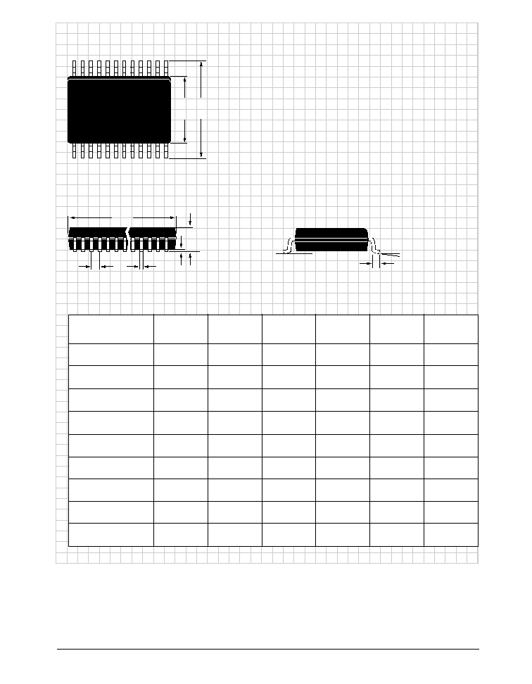
SP8542/8544DS/01 SP8542/8544 Two and Four Channel 12-Bit Multiplexed Sampling ADC's
© Copyright 2000 Sipex Corporation
15
D
E
H
PACKAGE: PLASTIC
SMALL OUTLINE (SOIC)
DIMENSIONS (Inches)
Minimum/Maximum
(mm)
14PIN
A
A1
Ø
L
B
e
A
A1
B
D
E
e
H
L
Ø
16PIN
0.090/0.104
(2.29/2.649)
0.004/0.012
(0.102/0.300)
0.013/0.020
(0.330/0.508)
0.398/0.413
(10.10/10.49)
0.291/0.299
(7.402/7.600)
0.050 BSC
(1.270 BSC)
0.394/0.419
(10.00/10.64)
0.016/0.050
(0.406/1.270)
0
°
/8
°
(0
°
/8
°
)
18PIN
0.090/0.104
(2.29/2.649))
0.004/0.012
(0.102/0.300)
0.013/0.020
(0.330/0.508)
0.447/0.463
(11.35/11.74)
0.291/0.299
(7.402/7.600)
0.050 BSC
(1.270 BSC)
0.394/0.419
(10.00/10.64)
0.016/0.050
(0.406/1.270)
0
°
/8
°
(0
°
/8
°
)
20PIN
0.090/0.104
(2.29/2.649)
0.004/0.012
(0.102/0.300)
0.013/0.020
(0.330/0.508)
0.496/0.512
(12.60/13.00)
0.291/0.299
(7.402/7.600)
0.050 BSC
(1.270 BSC))
0.394/0.419
(10.00/10.64)
0.016/0.050
(0.406/1.270)
0
°
/8
°
(0
°
/8
°
)
24PIN
0.090/0.104
(2.29/2.649)
0.004/0.012
(0.102/0.300)
0.013/0.020
(0.330/0.508)
0.599/0.614
(15.20/15.59)
0.291/0.299
(7.402/7.600)
0.050 BSC
(1.270 BSC)
0.394/0.419
(10.00/10.64)
0.016/0.050
(0.406/1.270)
0
°
/8
°
(0
°
/8
°
)
28PIN
0.090/0.104
(2.29/2.649)
0.004/0.012
(0.102/0.300)
0.013/0.020
(0.330/0.508)
0.697/0.713
(17.70/18.09)
0.291/0.299
(7.402/7.600)
0.050 BSC
(1.270 BSC)
0.394/0.419
(10.00/10.64)
0.016/0.050
(0.406/1.270)
0
°
/8
°
(0
°
/8
°
)
0.090/0.104
(2.29/2.649))
0.004/0.012
(0.102/0.300)
0.013/0.020
(0.330/0.508)
0.348/0.363
(8.83/9.22)
0.291/0.299
(7.402/7.600)
0.050 BSC
(1.270 BSC)
0.394/0.419
(10.00/10.64)
0.016/0.050
(0.406/1.270)
0
°
/8
°
(0
°
/8
°
)
SP8542/8544DS/01 SP8542/8544 Two and Four Channel 12-Bit Multiplexed Sampling ADC's
© Copyright 2000 Sipex Corporation
16
ORDERING INFORMATION
Model ..................................................... INL Linearity (LSB) ............................. Temperature Range ..................................... Package Types
SP8542JN ...........................................................
±
1.0 ................................................ 0°C to +70°C ................................. 16-pin, 0.3" Plastic DIP
SP8542JS ...........................................................
±
1.0 ................................................ 0°C to +70°C .......................................... 16-pin, 0.3" SOIC
SP8542KN .........................................................
±
0.75 ............................................... 0°C to +70°C ................................. 16-pin, 0.3" Plastic DIP
SP8542KS .........................................................
±
0.75 ............................................... 0°C to +70°C .......................................... 16-pin, 0.3" SOIC
SP8542AN ..........................................................
±
1.0 ............................................... -40°C to +85°C ............................... 16-pin, 0.3" Plastic DIP
SP8542AS ..........................................................
±
1.0 ............................................... -40°C to +85°C ........................................ 16-pin, 0.3" SOIC
SP8542BN .........................................................
±
0.75 .............................................. -40°C to +85°C ............................... 16-pin, 0.3" Plastic DIP
SP8542BS .........................................................
±
0.75 .............................................. -40°C to +85°C ........................................ 16-pin, 0.3" SOIC
Model ..................................................... INL Linearity (LSB) ............................. Temperature Range ..................................... Package Types
SP8544JN ...........................................................
±
1.0 ................................................ 0°C to +70°C ................................. 18-pin, 0.3" Plastic DIP
SP8544JS ...........................................................
±
1.0 ................................................ 0°C to +70°C .......................................... 18-pin, 0.3" SOIC
SP8544KN .........................................................
±
0.75 ............................................... 0°C to +70°C ................................. 18-pin, 0.3" Plastic DIP
SP8544KS .........................................................
±
0.75 ............................................... 0°C to +70°C .......................................... 18-pin, 0.3" SOIC
SP8544AN ..........................................................
±
1.0 ............................................... -40°C to +85°C ............................... 18-pin, 0.3" Plastic DIP
SP8544AS ..........................................................
±
1.0 ............................................... -40°C to +85°C ........................................ 18-pin, 0.3" SOIC
SP8544BN .........................................................
±
0.75 .............................................. -40°C to +85°C ............................... 18-pin, 0.3" Plastic DIP
SP8544BS .........................................................
±
0.75 .............................................. -40°C to +85°C ........................................ 18-pin, 0.3" SOIC
Please consult the factory for pricing and availability on a Tape-On-Reel option.
Corporation
SIGNAL PROCESSING EXCELLENCE
Sipex Corporation reserves the right to make changes to any products described herein. Sipex does not assume any liability arising out of the
application or use of any product or circuit described hereing; neither does it convey any license under its patent rights nor the rights of others.
Sipex Corporation
Headquarters and
Sales Office
22 Linnell Circle
Billerica, MA 01821
TEL: (978) 667-8700
FAX: (978) 670-9001
e-mail: sales@sipex.com
Sales Office
233 South Hillview Drive
Milpitas, CA 95035
TEL: (408) 934-7500
FAX: (408) 935-7600