1
Date: 5/25/04 SPX1202 600mA Low Dropout Positive Linear Regulator
© Copyright 2004 Sipex Corporation
600mA Low Dropout Linear Regulator
SPX1202
DESCRIPTION
FEATURES
Guaranteed 600mA Output
Three Terminal Adjustable or Fixed
2.5V, 3V and 3.3V
Low Quiescent Current
Low Dropout Voltage of 1.1V at Full Load
0.2% Line and 0.3% Load Regulation
Voltage Temperature Stability 0.05%
Overcurrent and Thermal Protection
Available Packages: SOT-223,TO-252,
TO-220, and TO-263
Æ
The SPX1202 is a low power positive-voltage regulator designed to satisfy moderate power
requirements with a cost effective, small footprint solution. This device is an excellent choice for
use in battery-powered applications and portable computers. The SPX1202 features very low
quiescent current and a low dropout voltage of 1.1V at a full load. As output current decreases,
quiescent current flows into the load, increasing efficiency. SPX1202 is available in adjustable
or fixed 2.5V, 3V and 3.3V output voltages.
The SPX1202 is offered in several 3-pin surface mount packages: SOT-223, TO-252, TO-220
and TO-263. An output capacitor of 10
µ
F provides unconditional stability while a smaller 2.2
µ
F
capacitor is sufficient for most applications.
APPLICATIONS
SCSI-II Active Terminator
Portable/ Palm Top / Notebook
Computers
Battery Chargers
Disk Drives
Portable Consumer Equipment
Portable Instrumentation
SMPS Post-Regulator
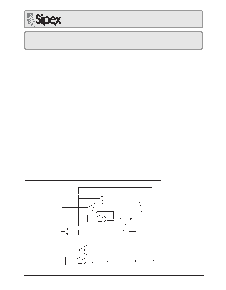
BLOCK DIAGRAM
+
-
Current Limit
I
CL
I
TL
Thermal Limit
V
REF
AMP
V
OUT
V
IN
ADJ/GND
I
ADJ
~50
µ
A
≠
Now Available in Lead Free Packaging
Refer to page 6 for pinouts.
2
Date: 5/25/04 SPX1202 600mA Low Dropout Positive Linear Regulator
© Copyright 2004 Sipex Corporation
at V
IN
=V
OUT
+ 1.5V, T
A
= 25
∞
C, C
IN
= C
OUT
= 10
µ
F, unless otherwise specified. Limits in Boldface applies over the
full operating temperature range.
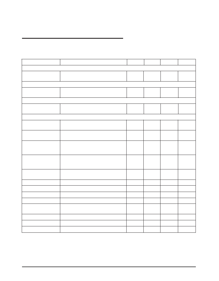
PARAMETER
CONDITIONS
TYP
MIN
MAX
UNITS
2.5V Version
Output Voltage
I
OUT
= 10mA, V
IN
= 5.00V
2.475
2.500
2.525
V
0
I
OUT
600mA, 4.50V
V
IN
10V
2.450
2.550
3.0V Version
Output Voltage
I
OUT
= 10mA, V
IN
= 5.00V
2.970
3.000
3.030
V
0
I
OUT
600mA, 4.50V
V
IN
10V
2.940
3.060
3.3V Version
Output Voltage
I
OUT
= 10mA, V
IN
= 5.00V
3.267
3.300
3.333
V
0
I
OUT
600mA, 4.50V
V
IN
10V
3.234
3.366
All Output Options
Reference Voltage
I
OUT
=10mA, (V
IN
- V
OUT
) = 2V
1.238
1.250
1.262
V
10
I
OUT
600mA, 1.4V
(V
IN
-V
OUT
)
10V
1.225
1.270
Output Voltage
(Note 1)
0.05
%
Temperature Stability
Line Regulation
4.50V
V
IN
12V,V
OUT
=3.00,I
OUT
=0
1.00
7.00
mV
4.80V
V
IN
12V,V
OUT
=3.30,I
OUT
=0
1.00
7.00
6.50V
V
IN
12V,V
OUT
=5.00,I
OUT
=0
1.00
10.00
Load Regulation
0
I
OUT
600mA,V
IN
=4.50V,V
OUT
=3.00
1.00
12.00
mV
0
I
OUT
600mA,V
IN
=4.80V,V
OUT
=3.30
1.00
12.00
0
I
OUT
600mA,V
IN
=6.50V,V
OUT
=5.0
1.00
15.00
Dropout Voltage
I
L
=100mA
1.00
1.10
V
(Note 2)
I
L
=600mA
1.05
1.15
Quiescent Current
4.25V
V
IN
6.5V
5.00
10.00
mA
Adjust Pin Current
50
µ
A
Current Limit
(V
IN
-V
OUT
)=5V
.850
1.0
A
Thermal Regulation
25
∞
C, 30mS Pulse
0.01
0.1
%/W
Ripple Rejection
f
RIPPLE
=120Hz, (V
IN
-V
OUT
)=3V,
60
75
dB
V
RIPPLE
=1V
PP
Long Term Stability
125
∞
C, 1000Hrs
0.03
%
RMS Output Noise
% of V
OUT
, 10Hz
f
10kHz
0.003
%
Thermal Resistance
Junction to Case, at tab
15
∞
C/W
ABSOLUTE MAXIMUM RATINGS
Power Dissipation ...................................... Internally Limited
Lead Temperature (soldering, 5 seconds) .................. 260
∞
C
Storage Temperature Range ...................... -65
∞
C to +150
∞
C
NOTES:
Note 1: Output temperature coefficient is defined as the worst case voltage change divided by the total temperature range.
Note 2: Dropout voltage is defined as the input to output differential at which the output voltage drops 100mV below its nominal value measured at 1V differential at
very low values of programmed output voltage, the minimum input supply voltage of 2V ( 2.3V over temperature) must be taken into account.
Note 3: Thermal regulation is defined as the change in output voltage at a time T after a change in power dissipation is applied excluding load or line regulation effect.
Operating Junction Temperature Range ..... -40
∞
C to +125
∞
C
Input Supply Voltage ..................................................... +20V
ESD Rating .............................................................. 2kV min
ELECTRICAL CHARACTERISTICS
3
Date: 5/25/04 SPX1202 600mA Low Dropout Positive Linear Regulator
© Copyright 2004 Sipex Corporation
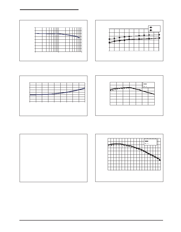
TYPICAL PERFORMANCE CHARACTERISTICS
Figure 1. Load Regulation for SPX1202M3-3.3;
Figure 2. Line Regulation for SPX1202M3-3.3;
V
IN
=4.8V, C
OUT
=2.2
µF
V
IN
=4.8V to 16V, C
OUT
=2.2
µF
Figure 3. Dropout Voltage vs Output Current for
SPX1202M3-3.3; V
IN
=4.89V, C
OUT
=2.2
µF
Figure 5. Current Limit for SPX1202M3-3.3, Output
Voltage Deviation with I
OUT
=10mA to 1A Step.
3.300
3.310
3.320
3.330
4.8
9.8
14.8
Vin (V)
V
out (V)
Series 1
Series 2
Line Regulation at 25
∞
C
0.9
1.0
1.1
1.2
1.3
100
200
300
400
500
600
700
800
900
1000
Output Current (mA)
Dropout V
oltage (V)
Figure 6. V
OUT
vs Temperature I
OUT
pilsed from 10mA to
Current Limit
Figure 4. Current Limit for SP1202M3-3.3; V
IN
=4.8V,
C
IN
=C
OUT
=1.0
µF, I
OUT
pulsed from 10mA to Current
Limit
Temp (
∞
C)
-50
-25
0
25
50
75
100
125
2.00
1.50
1.00
0.50
0.00
Series 1
Series 2
Current Limit (A)
Current Limit VS Temp
Temp (
∞
C)
-50
-30
-10
10
30
50
70
90
110
130
3.340
2.320
3.300
3.280
3.260
3.240
V
OUT
(V)
Series 1
Series 2
3.280
3.285
3.290
3.295
3.300
3.305
3.310
3.315
3.320
10
100
1000
Output Current (mA)
Output V
oltage (V)
SCOPE TRACING MISSING
4
Date: 5/25/04 SPX1202 600mA Low Dropout Positive Linear Regulator
© Copyright 2004 Sipex Corporation
APPLICATION INFORMATION
Output Capacitor
To ensure the stability of the SPX1202, an
output capacitor of at least 10
µF (tantalum or
ceramic)or 50
µF (aluminum) is required. The
value may change based on the application
requirements of the output load or temperature
range. The value of ESR can vary based on the
type of capacitor used in the applications. The
recommended value for ESR is 0.5
or less. A
larger value of output capacitance (up to 100
µF)
can improve the load transient response.
SOLDERING METHODS
The SPX1202 SOT-223 package is designed to
be compatible with infrared reflow or vapor-
phase reflow soldering techniques. During sol-
dering, the non-active or mildly active fluxes
may be used. The SPX1202 die is attached to
the heatsink lead which exits opposite the input,
output, and ground pins.
Hand soldering and wave soldering should be
avoided since these methods can cause damage
to the device with excessive thermal gradients
on the package. The SOT-223 recommended
soldering method are as follows: vapor phase
reflow and infrared reflow with the component
preheated to within 65
∞C of the soldering tem-
perature range
THERMAL CHARACTERISTICS
The thermal resistance of SPX1202 depends on
the type of package and PC board layout as
shown in Table 1. The SPX1202 features the
internal thermal limiting to protect the device
during overload conditions. Special care needs
to be taken during continuous load conditions
such that the maximum junction temperature
does not exceed 125
∞C. Thermal protection is
activated at >144
∞C and deactiviated at <137∞C.
Taking the FR-4 printed circuit board and 1/16
thick with 1 ounce copper foil as an experiment,
the PCB material is effective at transmitting
heat with the tab attached to the pad area and a
ground plane layer on the backside of the sub-
strate. Refer to table 1 for the results of the
experiment.
The thermal interaction from other components
in the application can effect the thermal resis-
tance of the SPX1202. The actual thermal resis-
tance can be determined with experimentation.
SPX1202 power dissipation is calculated as
follows:
P
D
= (V
IN
- V
OUT
)(I
OUT
)
Maximum Junction Temperature range:
T
J
= T
AMBIENT
(max) + P
D
* (Thermal Resistance)
(Junction-to-ambient)
Maximum junction temperature must not ex-
ceed the 125
∞C.
Ripple Rejection
Ripple rejection can be improved by adding a
capacitor between the ADJ pin and ground as
shown in Figure 7. When ADJ pin bypassing is
used, the value of the output capacitor required
increases to its maximum. If the ADJ pin is not
bypassed, the value of the output capacitor can
be lowered to 10
µF for an electrolytic aluminum
capacitor or 2.2
µF for a solid tantalum capacitor
(Fig 10).
However the value of the ADJ-bypass capacitor
should be chosen with respect to the following
equation:
C = 1 / ( 6.28 * F
R
* R
1
)
Where C = value of the capacitor in Farads
(select an equal or larger standard value),
F
R
= ripple frequency in Hz,
R
1
= value of resistor R
1
in Ohms.
If an ADJ-bypass capacitor is used, the ampli-
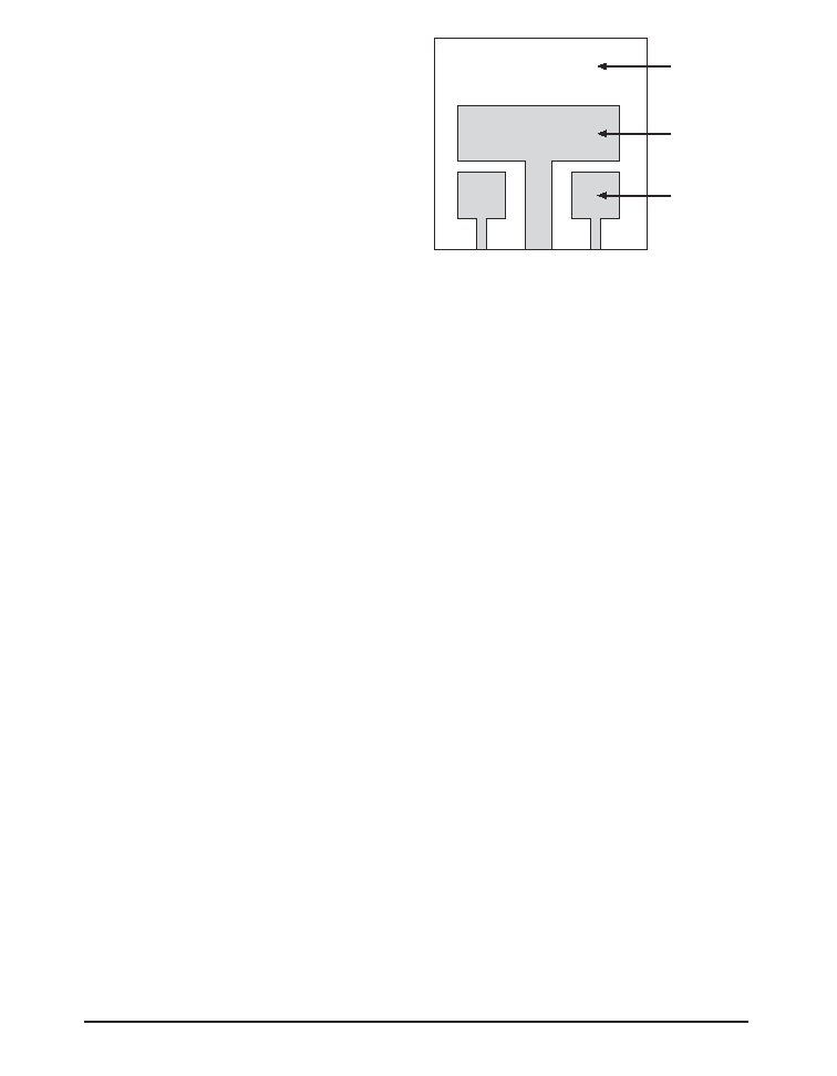
Figure 7. Substrate Layout for SOT-223
50 X 50mm
35 X 17mm
16 X 10mm

5
Date: 5/25/04 SPX1202 600mA Low Dropout Positive Linear Regulator
© Copyright 2004 Sipex Corporation
PC BOARD
TOPSIDE COPPER BACKSIDE COPPER
THERMAL RESISTANCE
AREA mm
2
AREA mm
2
AREA mm
2
JUNCTION TO AMBIENT
∞C/W
2500
2500
2500
46
2500
1250
2500
47
2500
950
2500
49
2500
2500
0
51
2500
1800
0
53
1600
600
1600
55
2500
1250
0
58
2500
915
0
59
1600
600
0
67
900
240
900
72
900
240
0
85
Figure 8. 600mA Current Source
Figure 9. Typical Adjustable Regulator
LOAD
ADJ
SPX1202
V
IN
C
1
OUT
IN
4.7
µ
F
C
2
I
OUT
R
1
V
REF
R
1
I
OUT
=
+
IN
OUT
I
ADJ
SPX1202
C
1
R
1
R
2
V
OUT
V
IN
C
2
V
OUT
= V
REF
(1+R
2
/R
1
) +I
ADJ
R
2
V
REF
50
µ
A
ADJ
4.7
µ
F +
tude of the output ripple will be independent of
the output voltage. If an ADJ-bypass capacitor
is not used, the output ripple will be proportional
to the ratio of the output voltage to the reference
voltage:
M = V
OUT
/ V
REF
Where M = multiplier for the ripple seen when
the ADJ pin is optimally bypassed.
V
REF
=1.25V
Output Voltage
The output of the adjustable regulator can be set
to any voltage between 1.25V and 15V. The
value of V
OUT
can be quickly approximated
using the formula. (Figure 9)
V
OUT
=1.25 *(R
1
+ R
2
)/R
1
.
A small correction to this formula is required
depending on the values of resistors R1 and R2,
since adjustable pin current (approx 50
µA) flows
through R2. When I
ADJ
is taken into account, the
formula becomes
V
OUT
= V
REF
(1+ (R
2
/R
1
)) + I
ADJ
* R
2
,
where V
REF
=1.25V.
TYPICAL APPLICATIONS
Table 1