 | –≠–ª–µ–∫—Ç—Ä–æ–Ω–Ω—ã–π –∫–æ–º–ø–æ–Ω–µ–Ω—Ç: SPX1432A | –°–∫–∞—á–∞—Ç—å:  PDF PDF  ZIP ZIP |
1
Rev. 6/16/03 SPX1432 1.24V Precision Adjustable Shunt Regulator
© Copyright 2003 Sipex Corporation
1.24V Precision Adjustable Shunt Regulator
SPX1432
DESCRIPTION
FEATURES
Reference Voltage: 1.24V
Initial Accuracy: 0.5%
Wide Operating Current, 60
µ
A to 100mA
Ultra Low Reference Input Current, 100nA
Output Voltage Range: V
REF
to 20V
0
∞
C to 105
∞
C Guaranteed Operation
SOT-23-3 Package
Upgrade to LMV431, TLV431, SC431L
Æ
The SPX1432 is a three terminal adjustable shunt voltage regulator that provides a highly accurate 1.24V
bandgap reference with 0.5% accuracy, eliminating the need for trimming in most power supply designs.
Offered in the tiny SOT-23 package, the SPX1432 has an extremely wide operating current range of 60uA
to 100mA, and reference input current of only 100nA (typ). The SPX1432 can regulate outputs from V
REF
to 20V, using two external resistors, and is guaranteed over the extended commercial temperature range
of 0
∞
C to 105
∞
C.
The combination of the small size, wide output current capability, flexible voltage range, and stable
performance over the entire extended commercial temperature range, makes the SPX1432 the ideal
candidate a variety of shunt regulator and current source designs in applications such as Portable meters,
Instrumentation, and Industrial Process Control.
APPLICATIONS
Switching Power Supplies
Adjustable Supplies
Error Amplifiers
Single Supply Amplifier
Monitors / VCRs / TVs
Personal Computers
Voltage References
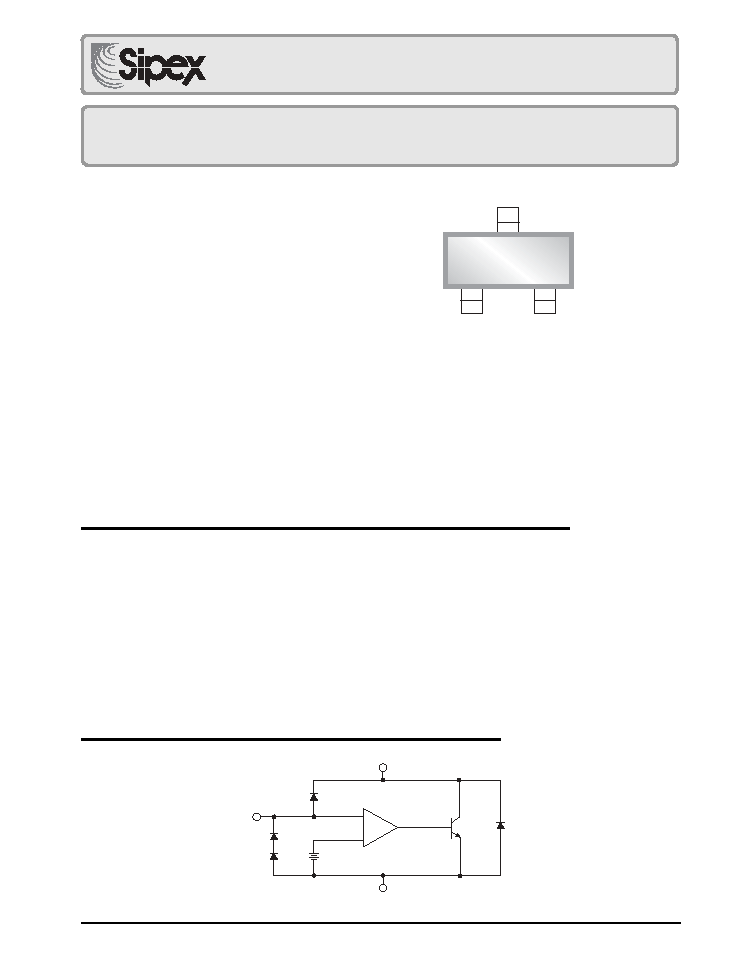
FUNCTIONAL DIAGRAM
+
-
1.24V
Reference
(R)
Anode (A)
Cathode (K)
1
3
2
SPX1432
ANODE
CATHODE
REF
1
2
3
2
Rev. 6/16/03 SPX1432 1.24V Precision Adjustable Shunt Regulator
© Copyright 2003 Sipex Corporation
Cathode-Anode Reverse Breakdown V
KZ
....................................... 22V
Anode-Cathode Forward Current, (<10ms) I
AK
................................. 1A
Operating Cathode Current I
KA
.................................................. 120mA
Reference Input Current I
REF
.......................................................... 1mA
Continuos Power Dissipation at 25
∞
C P
D
SOT-23 .................................................................. 200 mW
Junction Temperature T
J
........................................................... 150
∞
C
Storage Temperature T
STG
.............................................. -65 to 150
∞
C
Lead Temperature (Soldering 10 sec.) T
L
.................................. 300
∞
C
Stresses greater than those listed under ABSOLUTE MAXIMUM RATINGS may cause permanent damage to the device. This is a stress rating only
and functional operation of the device at these or any other conditions above those indicated in the operational sections of this specification is not
implied. Exposure to absolute maximum rating conditions for extended periods may affect reliability.
ELECTRICAL CHARACTERISTICS
Electrical characteristics are guaranted over the full junction temperature range (0
∞C to 105∞C). Ambient temperature must
be derated based upon power dissipation and package thermal characteristics. Unless otherwise specified, test conditions are:
V
KA
= V
REF
and I
K
= 10mA.
PARAMETER
SYMBOL
FIGURE CONDITIONS
MIN
TYP
MAX
UNITS
Accuracy 0.5%
SPX1432A
Output Voltage
V
REF
2
T
J
= 25
∞
C
1.234
1.240
1.246
V
Temperature Deviation
V
REF
2
0 < T
J
< 105
∞
C
6
12
mV
Line Regulation
V
REF
3
V
KA
= 1.25V to 15V
15
37
mV
Load Regulation
V
REF
2
I
K
= 100
µ
A to 100mA
10
30
mV
Reference Input Current
I
REF
3
T
J
= 25
∞
C, R1 = 10K
, R2 =
0.1
0.3
µ
A
Reference Input Current
I
REF
3
0 < T
J
< 105
∞
C,
0.05
0.2
µ
A
Temperature Coefficient
R1 = 10K
, R2 =
Minimim Cathode
I
K(MIN)
2
T
J
= 25
∞
C
60
80
µ
A
Current for Regulation
Off State Leakage
I
K(MIN)
4
V
REF
= 0V, V
KA
= 18V, T
J
= 25
∞
C
0.01
500
nA
PARAMETER
SYMBOL
FIGURE CONDITIONS
MIN
TYP
MAX
UNITS
Accuracy 1.0%
SPX1432
Output Voltage
V
REF
2
T
J
= 25
∞
C
1.228
1.240
1.252
V
Temperature Deviation
V
REF
2
0 < T
J
< 105
∞
C
9
18
mV
Line Regulation
V
REF
3
V
KA
= 1.25V to 15V
15
37
mV
Load Regulation
V
REF
2
I
K
= 100
µ
A to 100mA
10
30
mV
Reference Input Current
I
REF
3
T
J
= 25
∞
C, R1 = 10K
, R2 =
0.1
0.5
µ
A
Reference Input Current
I
REF
3
0 < T
J
< 105
∞
C,
0.05
0.4
µ
A
Temperature Coefficient
R1 = 10K
, R2 =
Minimim Cathode
I
K(MIN)
2
T
J
= 25
∞
C
60
100
µ
A
Current for Regulation
Off State Leakage
I
K(MIN)
4
V
REF
= 0V, V
KA
= 18V, T
J
= 25
∞
C
0.01
500
nA
RECOMMENDED CONDITIONS
PARAMETER
SYMBOL
RATING
UNIT
Cathode Voltage
V
KA
V
REF
to 20
V
Cathode Current
I
K
10
mA
TYPICAL THERMAL RESISTANCES
PACKAGE
JA
JC
TYPICAL
DERATING
SOT-23
575
∞
C/W
150
∞
C/W
1.7 mW/
∞
C
Typical deratings of the thermal resistances are given for ambient
temperature >25
∞
.
ABSOLUTE MAXIMUM RATINGS
3
Rev. 6/16/03 SPX1432 1.24V Precision Adjustable Shunt Regulator
© Copyright 2003 Sipex Corporation
0
5000
ppm
0
0.5
%
27ppm/
∞
C
0.0027% /
∞
C
0.0033mV /
∞
C
0
15
30
45
60
75
90
105
0
mV
-5
T
V
REF
Junction Temperature (
∞
C)
V
REF
(mV)
T
A
(
V
REF
at 25
∞
C
)
T
A
V
REF
x 100
∑
TC in % /
∞
C =
∑
TC in mV /
∞
C =
(
V
REF
at 25
∞
C
)
T
A
V
REF
x 10
6
∑
TC in ppm /
∞
C =
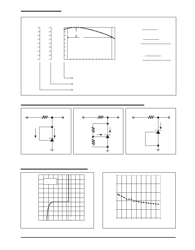
CALCULATION AVERAGE TEMPERATURE COEFICIENT (TC)
Figure 1. V
REF
VS Temperature.
TEST CIRCUITS
I
REF
V
KA =
V
REF
V
IN
I
K
I
REF
V
KA
V
IN
I
K
(V
REF
)
R1
R2
V
KA
V
IN
I
K (OFF)
Figure 2. Test Circuit for V
KA
= V
REF
Figure 3. Test Circuit for V
KA
> V
REF
Figure 4. Test Circuit for I
KOFF
-2
-1
0
1
2
3
1.24
15.0
12.5
10.0
7.5
5.0
2.5
0
-2.5
-5.0
-7.5
-10.0
V
KA
Cathode Voltage (V)
I
K
Cathode Current (mA)
V
KA
= V
REF
25
∞
C
TYPICAL PERFORMANCE CHARACTERISTICS
High Current Operating Characteristics.
Reference Input Current VS Ambient Temperature.
0
40
80
120
160
200
-60
-40
-20
0
20
40
60
80
100 120
T
A
-Ambient Temperature (∞C)
I
REF
-Reference Input Current (nA)
4
Rev. 6/16/03 SPX1432 1.24V Precision Adjustable Shunt Regulator
© Copyright 2003 Sipex Corporation
1.235
1.24
1.245
1.25
0.01
0.1
1
10
100
Ik--cathode Current (mA)
V
KA
--Cathode V
oltage (V)
-40
-30
-20
-10
0
0
3
6
9
12
15
18
21
V
KA
-Cathode Voltage (V)
D
VREF
(mV)
0.0001
0.0010
0.0100
0.1000
1.0000
10.0000
100.0000
1000.0000
-50
0
50
100
150
Ta Ambient Temperature (C)
Ikoff Cathode Current (nA)
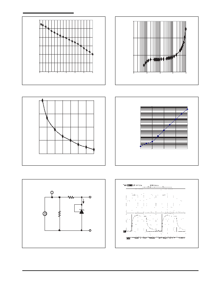
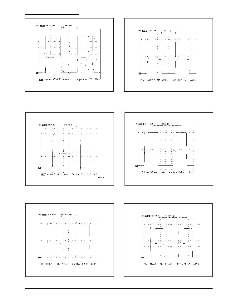
Reference Voltage VS Ambient Temperature.
Reference Voltage Load Regulation.
Reference Voltage Line Regulation.
Off State Leakage VS Ambient Temperature.
1.22
1.225
1.23
1.235
1.24
1.245
1.25
-60
-30
0
30
60
90
120
T
A
-Ambient Temperature (∞C)
V
REF
-Reference V
o
ltage (V)
Ch1-V
IN
Ch2-V
KA
I
KA
= 0 to 100
µA.
GND
V
IN
f
P
= 100kHz
50
R
V
OUT
I
K
Test Circuit for Pulse Response.
TYPICAL PERFORMANCE CHARACTERISTICS: Continued
5
Rev. 6/16/03 SPX1432 1.24V Precision Adjustable Shunt Regulator
© Copyright 2003 Sipex Corporation
I
KA
= 0 to 300
µA.
I
KA
= 0 to 1mA.
I
KA
= 0 to 10mA.
I
KA
= 0 to 50mA.
TYPICAL PERFORMANCE CHARACTERISTICS: Continued
I
KA
= 0 to 100mA
I
KA
= 0 to 80mA
6
Rev. 6/16/03 SPX1432 1.24V Precision Adjustable Shunt Regulator
© Copyright 2003 Sipex Corporation
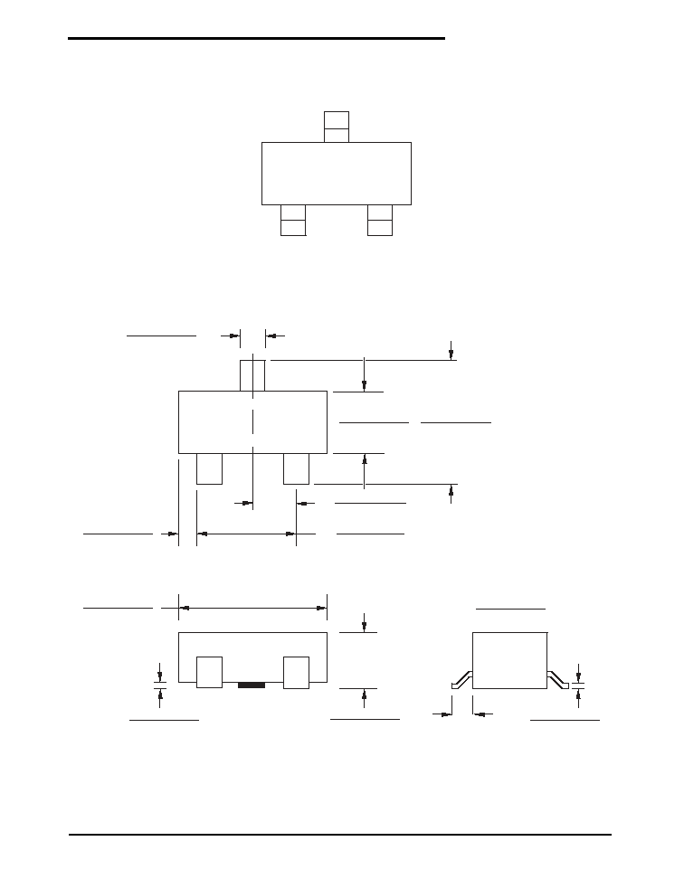
PACKAGE: 3 PIN SOT23
SOT23-3 (M)
0.015 - 0.018
(0.381 - 0.457)
0.020 - 0.024
(0.508 - 0.610)
0.110 - 0.120
(2.794 - 3.048)
0.001 - 0.004
(0.025 - 0.102)
0.030 - 0.041
(0.762 - 1.041)
0.018 - 0.024
(0.457 - 0.610)
0.070 - 0.080
(1.778 - 2.032)
0.035 - 0.040
(0.889 - 1.016)
0.047 - 0.055
(1.194 - 1.397)
0.083 - 0.098
(2.108 - 2.489)
0.003 - 0.005
(0.076 - 0.127)
ANODE
CATHODE
REF
1
3
2
Top View
7
Rev. 6/16/03 SPX1432 1.24V Precision Adjustable Shunt Regulator
© Copyright 2003 Sipex Corporation
Corporation
ANALOG EXCELLENCE
Sipex Corporation reserves the right to make changes to any products described herein. Sipex does not assume any liability arising out of the
application or use of any product or circuit described herein; neither does it convey any license under its patent rights nor the rights of others.
Sipex Corporation
Headquarters and
Sales Office
233 South Hillview Drive
Milpitas, CA 95035
TEL: (408) 934-7500
FAX: (408) 935-7600
Sales Office
22 Linnell Circle
Billerica, MA 01821
TEL: (978) 667-8700
FAX: (978) 670-9001
e-mail: sales@sipex.com
PART NUMBER
ACC
OUTPUT VOLTAGE
TOP MARK
PACKAGES
SPX1432AM ............ 0.5% .................. 1.24V .......................... W1 ............ 3-Pin SOT-23
SPX1432M ............... 1.0% .................. 1.24V ........................... F2 ............ 3-Pin SOT-23
ORDERING INFORMATION