1
Rev. 08/13/02 SPX2431L Precision Adjustable Shunt Regulator
© Copyright 2002 Sipex Corporation
Precision Adjustable Shunt Regulator
SPX2431L
DESCRIPTION
FEATURES
Trimmed Bandgap to 0.5% and 1.0%
Wide Operating Current 160
µ
A to 100mA
Extended Temperature Range:
0
∞
C to 105
∞
C
Low Temperature Coefficient 30 ppm/
∞
C
Offered in TO-92, SOIC, SOT-23-3
Replacement for TL431 and AS2431L
Low Cost Solution
Æ
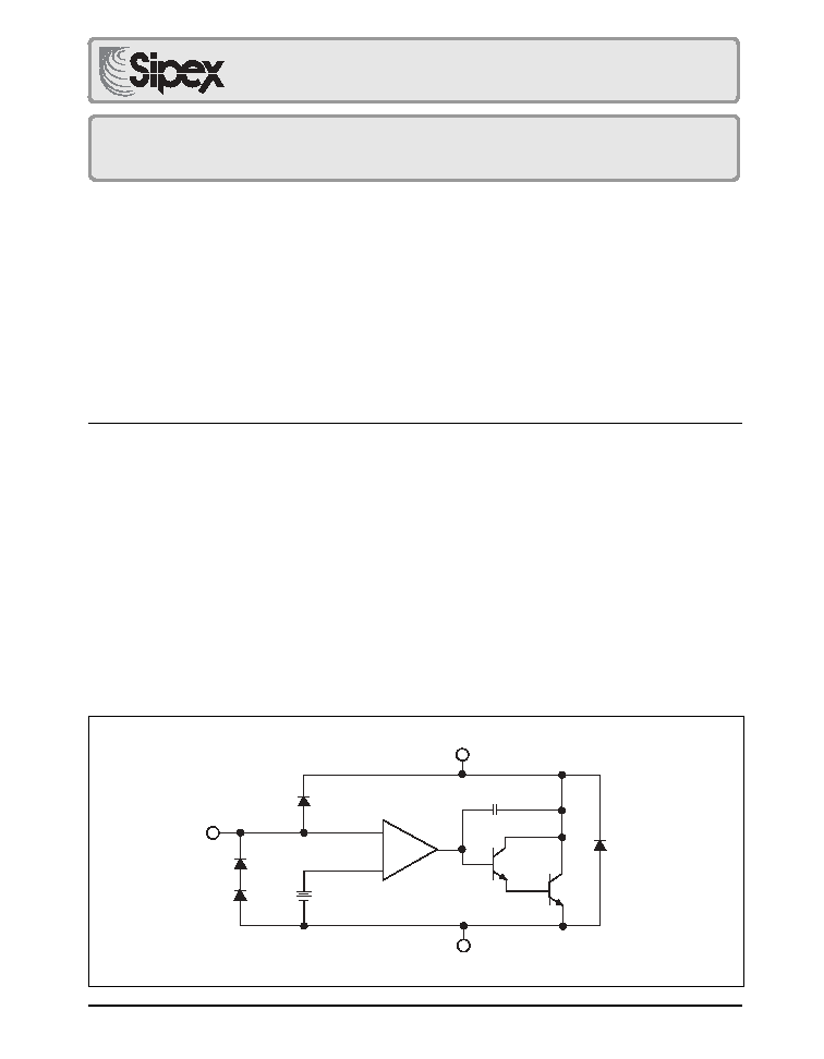
The SPX2431L is a 3-terminal adjustable shunt voltage regulator providing a highly accurate
bandgap reference (0.5%) and extremely low operating current (100
µ
A). The SPX2431L acts
as an open-loop error amplifier with a 2.5V temperature compensated reference. The
SPX2431L's thermal stability, wide operating current (100mA) and temperature range (0
∞
C to
150
∞
C) makes it suitable for a variety of applications. SPX2431LA tolerance of 0.5% is proven
to be sufficient to overcome all the other errors in the system to virtually eliminate the need for
trimming in the power supply manufacturer's assembly lines and contributes a significant cost
savings.
In the standard shunt configuration, the combination of a low temperature coefficient, sharp
turn on characteristics, low output impedance, and programmable output voltage makes this
precision reference an excellent error amplifier. The SPX2431L is available in TO-92, SOIC-8,
and SOT-23-3 package.
APPLICATIONS
Battery Operating Equipment
Adjustable Supplies
Switching Power Supplies
Error Amplifiers
Single Supply Amplifier
Monitors / VCRs / TVs
Personal Computers
BLOCK DIAGRAM
+
-
2.5V
Reference
(R)
Anode (A)
Cathode (K)
2
Rev. 08/13/02 SPX2431L Precision Adjustable Shunt Regulator
© Copyright 2002 Sipex Corporation
ABSOLUTE MAXIMUM RATINGS
Cathode-Anode Reverse Breakdown V
KA
....................................... 20V
Anode-Cathode Forward Current, (<10ms) I
AK
................................. 1A
Operating Cathode Current I
KA
.................................................. 100mA
Reference Input Current I
REF
....................................................... 1.0mA
Continuos Power Dissipation at 25
∞
C P
D
TO-92 ..................................................................... 775mW
SOT-23 .................................................................. 200 mW
SOIC-8 .................................................................... 750mW
Junction Temperature T
J
........................................................... 150
∞
C
Storage Temperature T
STG
.............................................. -65 to 150
∞
C
Lead Temperature (Soldering 10 sec.) T
L
.................................. 300
∞
C
NOTE: Stresses greater than those listed under ABSOLUTE MAXIMUM
RATINGS may cause permanent damage to the device. This is a stress
rating only and functional operation of the device at these or any other
conditions above those indicated in the operational sections of this
specification is not implied. Exposure to absolute maximum rating condi-
tions for extended periods may affect reliability.
TYPICAL THERMAL RESISTANCES
PACKAGE
0
JA
0
JC
TYPICAL DERATING
TO-92
160
∞
C/W 80
∞
C/W
6.3 mW/
∞
C
SOT-23
575
∞
C/W 150
∞
C/W
1.7 mW/
∞
C
SOIC-8
175
∞
C/W 45
∞
C/W
5.7 mW/
∞
C
Typical deratings of the thermal resistances are given for ambient
temperature >25
∞
.
ELECTRICAL CHARACTERISTICS
Electrical characteristics at 25
∞C I
K
= 10mA V
K
= V
REF
, unless otherwise specified.
PARAMETER
SYMBOL FIGURE CONDITIONS
MIN
TYP
MAX
MIN
TYP
MAX
UNITS
SPX2431LA
SPX2431
Reference Voltage
V
REF
2
2.490
2.503
2.515
2.470
2.495
2.520
V
2
T
J
= 0
∞
C to 150
∞
C
2.469
2.536
2.449
2.541
V
V
REF
withTemp.*
TC
2
0.07
0.20
0.07
0.20
mV/
∞
C
Ratio of Change in V
REF
V
REF
V
REF
to 10V
-2.7
-1.01
-2.7
-1.01
mV/V
to Cathode Voltage
V
K
3
10V to 20V
-2.0
-0.4
0.3
-2.0
-0.4
0.3
Reference Input Current
I
REF
3
0.7
4.0
0.7
4.0
µ
A
I
REF
Temp Deviation
I
REF
3
T
J
= 0
∞
C to 105
∞
C
0.4
1.2
0.4
1.2
µ
A
Min I
K
for Regulation
I
K(MIN)
2
160
160
µ
A
Off State Leakage
I
K(OFF)
4
V
REF
= 0V,
0.04
500
0.04
500
nA
V
KA
= 20V
Dynamic Output
Z
KA
2
z
1kHz
0.15
0.5
0.15
0.5
Impedance
I
K
= 0.16 to 100mA
Operating Range (T
J
) = -40
∞
C to 125
∞
C.
* See appropiate test circuit (Figure 2)
RECOMMENDED CONDITIONS
PARAMETER
SYMBOL
RATING
UNIT
Cathode Voltage
V
KA
V
REF
to 20
V
Cathode Current
I
K
10
mA
3
Rev. 08/13/02 SPX2431L Precision Adjustable Shunt Regulator
© Copyright 2002 Sipex Corporation
T
V
REF
0
15
30
45
60
75
90
105
-10
0.5
5000
0
0
0
0.07 mV/
∞
C
0.003 %/
∞
C
27 ppm/
∞
C
ppm
%
mV
Junction Temperature (
∞
C)
∑
TC in ppm/
∞
C =
∑
TC in %/
∞
C =
∑
TC in mV/
∞
C =
V
REF
(mV)
T
A
(
V
REF
at 25
∞
C
)
T
A
V
REF
x 100
(
V
REF
at 25
∞
C
)
T
A
V
REF
x 10
6
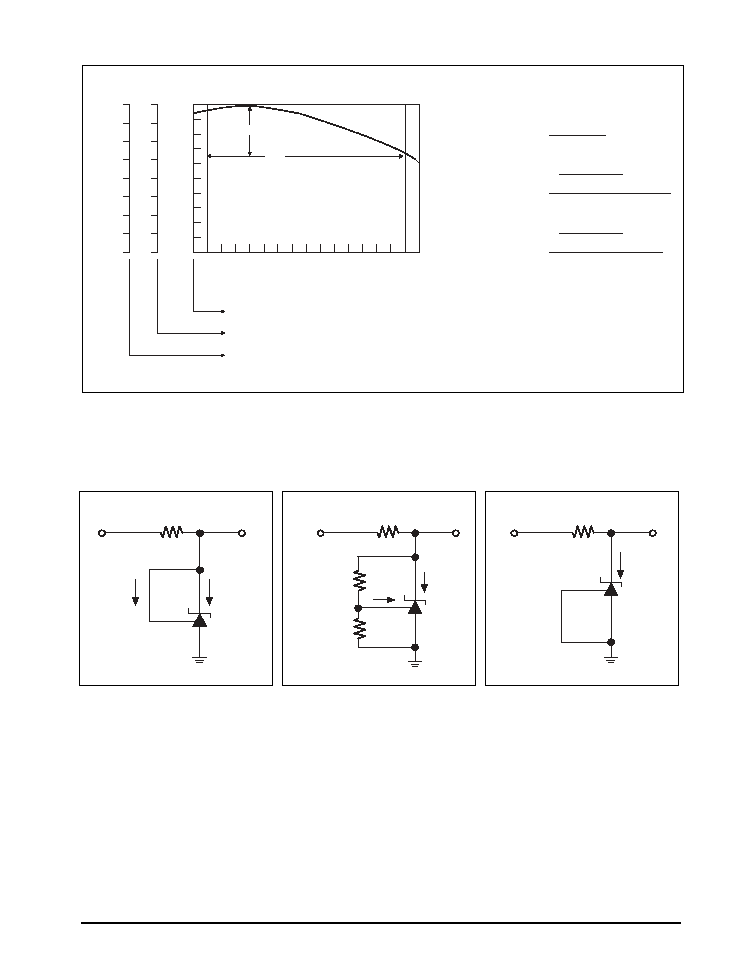
CALCULATING AVERAGE TEMPERATURE COEFFICIENT (TC)
Figure 1. V
REF
VS Temperature.
TEST CIRCUITS
I
REF
V
KA =
V
REF
V
IN
I
K
I
REF
V
KA
V
IN
I
K
(V
REF
)
R1
R2
V
KA
V
IN
I
K (OFF)
Figure 2. Test Circuit for V
KA
= V
REF
Figure 3. Test Circuit for V
KA
> V
REF
Figure 4. Test Circuit for I
KOFF
4
Rev. 08/13/02 SPX2431L Precision Adjustable Shunt Regulator
© Copyright 2002 Sipex Corporation
-2
-1
0
1
2
3
150
125
100
75
50
25
0
-25
-50
-75
-100
V
KA
Cathode Voltage (V)
I
K
Cathode Current (mA)
V
KA
= V
REF
0
∞
C to 105
∞
C
-60
-30
0
30
60
90
120
2.53
2.52
2.51
2.50
2.49
2.48
2.47
2.46
2.45
T
A
Ambient Temperature (
∞
C)
V
REF
Reference V
o
ltage (V)
V
KA
= V
REF
I
K
= 10mA
TYPICAL PERFORMANCE CHARACTERISTICS
Figure 5. High Current Operating Characteristics
Figure 6. Reference Voltage VS Ambient Tempetature
-1.0
0
1.0
2.0
3.0
270
240
210
180
150
120
90
60
30
0
-30
-60
V
KA
Cathode Voltage (V)
I
K
Cathode Current (
µ
A)
V
KA
= V
REF
0
∞
to 105
∞
C
105
∞
C
25
∞
C
-0
∞
C
-60
-30
0
30
60
90
120
3.0
2.5
2.0
1.5
1.0
0.5
0
T
A
Ambient Temperature (
∞
C)
I
REF
Reference Input Current (
µ
A)
R1 = 10k
R2 =
I
K
= 10mA
Figure 7. Low Current Operating Characteristics
Figure 8. Reference Input Current VS Ambient
Temperature
0
3
6
9
12 15
18
21
24
27 30
0
-10
-20
-30
-40
-50
V
KA
Cathode Voltage (V)
V
REF
(mV)
0
∞
C
25
∞
C
75
∞
C
125
∞
C
I
KA
= 10mA
Figure 9. Reference Voltage Line Regulation VS
Cathode Voltage and T
AMBIENT
10
100
1K
10K
100K
70
60
50
40
30
20
10
0
f Frequency (Hz)
Noise V
o
ltage nV/Hz
V
KA
= V
REF
I
K
= 10mA
T
A
= 25
∞
C
Figure 10. Noise Voltage VS Frequency
5
Rev. 08/13/02 SPX2431L Precision Adjustable Shunt Regulator
© Copyright 2002 Sipex Corporation
V
IN
V
OUT
V
IN
V
OUT
TYPICAL PERFORMANCE CHARACTERISTICS (continued)
-60
-30
0
30
60
90
120
0.150
0.125
0.100
0.075
0.050
0.025
0.0
T
A
Free Air Temperature
Z
KA
Dynamic Impedance (
)
V
KA
= V
REF
I
K
= 160
µ
to 100mA
f
1kHz
Figure 11. Low Frequency Dynamic Output Impedance
VS T
AMBIENT
10
100
1K
10K
100K
1M
10M
START 10.000Hz
STOP 50 000 000.000Hz
REF LEVEL
60.000dB
0.0deg
/DIV
10.000dB
45.000deg
MARKER 3 039
MAG (A/R)
MARKER 3 039
PHASE (A/R)
642.400Hz
0.057dB
6642.400Hz
81.770deg
GAIN
PHASE
60dB
50dB
40dB
30dB
20dB
10dB
0dB
-10dB
-20dB
-30dB
-40dB
215
∞
180
∞
135
∞
90
∞
45
∞
0
∞
-45
∞
-90
∞
-135
∞
-180
∞
-215
∞
Figure 12. Small Signal Gain and Phase VS Frequency;
I
K
= 10mA, T
A
= 25
∞C
I
K
V
IN
9
µ
F
15k
8.25k
V
OUT
GND
230
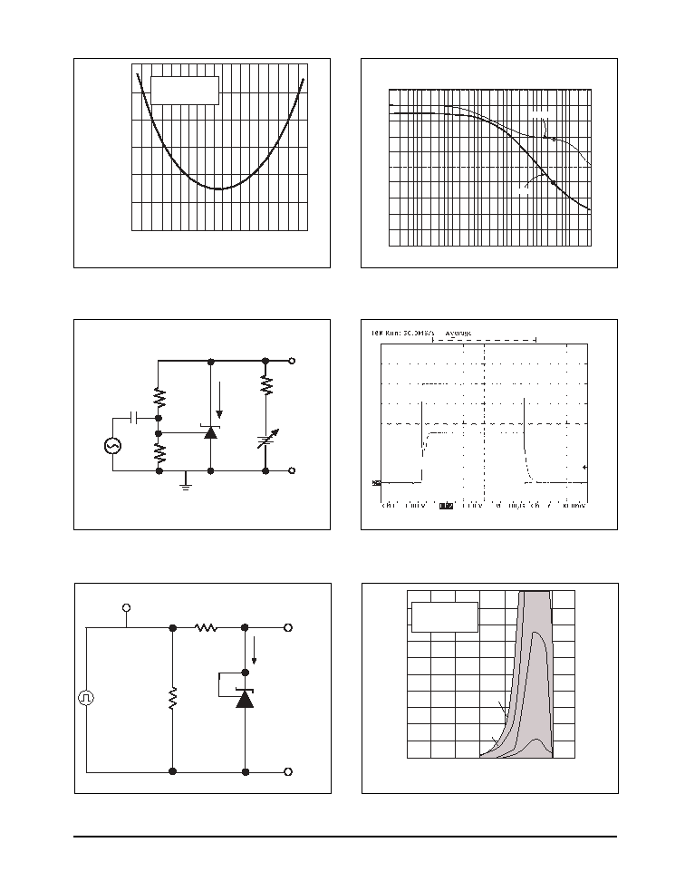
Figure 13. Test Circuit for Gain and Phase Frequency
Response
Figure 14. Frequency = 100kHz, I
K
= 10mA, T
A
= 25
∞C
Figure 15. Test Circuit for Pulse Response
Figure 16. Stability Boundary Conditions
I
K
V
OUT
GND
250
50
V
IN
f
p = 100kHz
10
0
10
1
10
2
10
3
10
4
10
5
10
6
10
7
100
90
80
70
60
50
40
30
20
10
0
C
L
Load Capacitance (pF)
I
K
Cathode Current (mA)
A: V
KA
= V
REF
B: V
KA
= 5V at I
K
=10mA
C: V
KA
=10V at I
K
=10mA
D: V
KA
=15V at I
K
=10mA
C
D
B
A
STABLE
STABLE
T
A = 25
∞
C