Rev. 12/7/00
SPX2730/31/32/33
3A High Current Low Dropout Voltage Regulator
Adjustable & Fixed Output,
Fast Response
(ADVANCED INFORMATION)
FEATURES
APPLICATIONS
∑ Adjustable Output Down To 1.2V
∑ Powering VGA & Sound Card
∑ 1% output accuracy @ 3.3V, 5.0V
∑ Power PCSupplies
∑ Output Current of 3A
∑ SMPS Post-Regulator
∑ Low Dropout Voltage 370mV(Typ.) @ 3A.
∑ High Efficiency "Green" Computer Systems
∑ Extremely Tight Load And Line Regulation
∑ High Efficiency Linear Power Supplies
∑ Extremely Fast Transient Response
∑ Portable Instrumentation
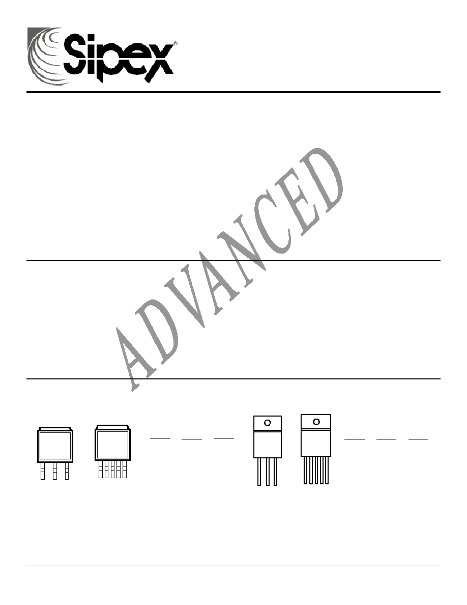
∑ Standard 3-Terminal Low Cost TO-220, TO-263
∑ Constant Current Regulators
∑ Reverse-battery and "Load Dump" Protection
∑ Adjustable Power Supplies
∑ Zero Current Shutdown Mode (5-Pin Versions)
∑ Battery charger
∑ Error Flag Signal Output Out-of Regulation (5-Pin Versions)
PRODUCT DESCRIPTION
The SPX2730/31/32/33 is a 3A high accuracy, low dropout voltage regulator (370mV(Typ)@ 3A). The SPX2730/31/32/33 is
designed for low voltage application that requires lower dropout voltage and faster transient response. This device is an excellent
choice for use in powering low voltage microprocessor that require a lower dropout, faster transient response to regulate from +2.5V
to 3.8V supplies and as a post regulator for switching supplies applications.
The SPX2730/31/32/33 offers full protection against over-current faults, reversed input polarity, reversed load insertion, and positive
and negative transient voltage. On-Chip trimming adjusts the reference voltage to 1%. Features such as enable pin, Error flag pin are
also included in the 5-pin package.
The SPX2730/31/32/33 are offered in 3 & 5 pin TO-220 & TO-263 packages compatible with other 3 terminal regulators.
PIN CONNECTIONS
Top View
TO-263-3 (T)
1
SPX2730
2
3
TO-263-5 (T)
Top View
4 5
SPX2731/32/33
1 2 3
Front View
TO-220-3 (U)
SPX2730
1
2
3
TO-220-5 (U)
Front View
5
4
3
2
1
SPX2731/32/33
SPX2731
SPX2732
SPX2733
1) ENABLE
2) INPUT
3) GND
4) OUTPUT
5) FLAG
1) ENABLE
2) INPUT
3) GND
4) OUTPUT
5) ADJUST
1) FLAG
2) INPUT
3) GND
4) OUTPUT
5) ADJUST
SPX2731
SPX2732
SPX2733
1) ENABLE
2) INPUT
3) GND
4) OUTPUT
5) FLAG
1) ENABLE
2) INPUT
3) GND
4) OUTPUT
5) ADJUST
1) FLAG
2) INPUT
3) GND
4) OUTPUT
5) ADJUST
Rev. 12/7/00
SPX2730/31/32/33
ABSOLUTE MAXIMUM RATINGS
Lead Temp. (Soldering, 5 Seconds) ................................ 260∞C
Maximum Input Voltage ...................................... 16V
Storage Temperature Range ......................................................-65∞ to +150∞C
Operating Junction Temperature Range
SPX2730/31/32/33 Control Section ................................ -45∞C +125∞C
SPX2730/31/32/33 Power Transistor............................... -45∞C +150∞C
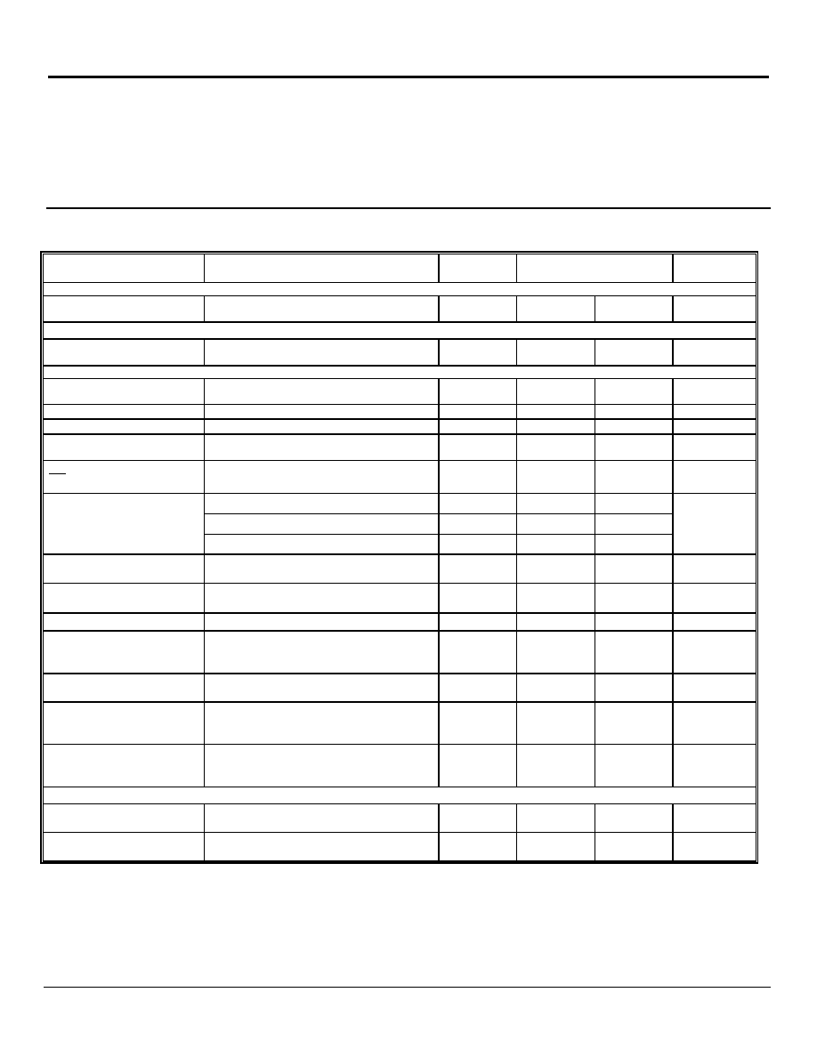
ELECTRICAL CHARACTERISTICS
(NOTE 1) at I
OUT
= 10mA, T
a
=25
∞C, unless otherwise specified.
PARAMETER
CONDITIONS Typ
SPX2730/31/32/33
Min Max
Units
3.3V Version
Output Voltage (Note 2)
I
OUT
= 10mA
10mA
I
OUT
3A, 4.75VV
IN
16V
3.3
3.3
3.270
3.240
3.330
3.360
V
5.0V Version
Output Voltage (Note 2)
I
OUT
= 10mA
10mA
I
OUT
3A, 5.5VV
IN
16V
5.0
5.0
4.95
4.90
5.05
5.10
V
All Voltage Options
Reference Voltage
1.240
1.228
1.215
1.252
1.265
V
Reference Voltage
(Note 8)`
1.203 1.277 V
Line Regulation
I
O
= 10mA, (V
OUT
+ 1V)
V
IN
16V
0.06
0.5 %
Load Regulation
V
IN
= V
OUT
+ 5V, 10mA
I
OUT
I
FULLLOAD
(Note 2, 6)
0.2 1 %
V
20
100
ppm/
∞C
T
Output Voltage (Note 6)
Temperature Coef.
I
O
= 100mA
80 175
I
O
= 1.5A
250
Dropout Voltage
I
O
= 3A
370 600
mV
Ground Current
I
O
= 1.5A, V
IN
= V
OUT
, +1V
I
O
= 3A
10
37
35
mA
I
GNDDO
Ground Pin Current at
Dropout
V
IN
= 0.5V less than specified V
OUT
I
OUT
= 10mA
0.9
mA
Current Limit
V
OUT
= 0V (Note 4)
4.5
3.0
A
Output Noise Voltage
(10Hz to 100kHz)
I
L
= 100mA
C
L
= 10
µF
C
L
= 33
µF
400
260
V
RMS
Adjust Pin
Bias Current
40
80
120
nA
Reference Voltage
Temperature
Coefficient
(Note 7)
20
ppm/
∞C
Adjust Pin Bias
Current Temperature
Coefficient
0.1
nA/
∞C
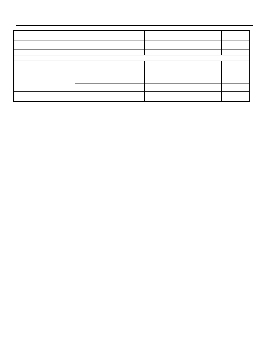
Flag Output (Error Comparator) SPX2731/SPX2733
Output Leakage
Current
V
OH
= 16V
0.01
1.00
2.00
µA
Output Low
Voltage
Device set for 5V. V
IN
= 4.5V
I
OL
= 250
µA
220 300
400
mV
Rev. 12/7/00
SPX2730/31/32/33
(Cont.)
Upper Threshold
Voltage
Device set for 5V (Note 9)
60
40
25
mV
Lower Threshold
Voltage
Device set for 5V (Note 9)
75
95
140
mV
Hysteresis
Device set for 5V (Note 9)
15
mV
ENABLE Input SPX2731/SPX2732
Input Logic Voltage
Low (OFF)
High (ON)
2.4
0.8
V
V
EN
= 16V
100
600
750
V
Enable Pin
Input Current
V
EN
= 0.8V
1
2
µA
Regulator Output
Current in Shutdown
(Note 10)
10
500
µA
Notes:
The Bold specifications apply to the full operating temperature range.
Note 1: Maximum positive supply voltage of 60V must be of limited duration (<100msec) and duty cycle.) The maximum continuous supply voltage is 16V.
Note 2: Full load current (I
FL
) is defined as 1.5A for the
Note 3: Dropout voltage is defined as the input-to output differential when the output voltage drops to 99% of its nominal value with V
OUT
+ 1V applied to V
IN
.
Note 4: V
IN
= V
OUT
(NOMINAL)
+1V. For example, use V
IN
= 4.3V for a3.3V regulator. Employ pulse-testing procedures to minimize temperature rise.
Note 5: Ground pin current is the regulator quiescent current. The total current drawn from the source is the sum of the load current to the ground current.
Note 6: Output voltage temperature coefficient is defined as the worst case voltage changed divided by the total temperature range.
Note 7: Thermal regulation is defined as the change in the output voltage at a time T after a change in power dissipation is applied, excluding load or line regulation
effects. Specifications are for a 200mA load pulse as V
IN
= 20V (a 4W pulse) for T = 10ms.
Note 8: V
REF
V
OUT
(V
IN
≠ 1), 2.3V
V
IN
16V, 10mA < IL I
FL
, TJ
T
JMAX
Note 9: Comparator threshold is expressed in terms of a voltage differential at the Adjust terminal below the nominal reference voltage measured a 6V input. To
express these thresholds in terms of output voltage change, multiply the error amplifier gain = V
OUT
/V
REF
= (R1 + R2)R2. For example, at a programmable output
voltage of 5V, the Error output is guaranteed to go low when the output drops by 95mVx 5V/ 1.240V = 38mV. Threshold remain constant as a percent of V
OUT
as V
OUT
is varied, with the dropout warning occurring at typically 5% below nominal, 7.7% guaranteed.
Note 10: V
EN
0.8V and V
IN
16V, V
OUT
= 0.
Rev. 12/7/00
SPX2730/31/32/33
APPLICATION HINTS
The SPX2730/31/32/33 incorporates protection against over-
current faults, reversed load insertion, over temperature
operation, and positive and negative transient voltage.
However, the use of an output capacitor is required in order to
insure the stability and the performances.
Thermal Consideration
Although the SPX2730/31/32/33 offers limiting circuitry for
overload conditions, it is necessary not to exceed the
maximum junction temperature, and therefore to be careful
about thermal resistance. The heat flow will follow the lowest
resistance path, which is the Junction-to-case thermal
resistance. In order to insure the best thermal flow of the
component, a proper mounting is required. Note that the case
of the device is electrically connected to the output. The
case has to be electrically isolated, a thermally conductive
spacer can be used. However do not forget to consider its
contribution to thermal resistance.
Assuming:
V
IN
= 10V, V
OUT
= 5V, I
OUT
= 1.5A, T
A
= 50
∞C/W,
Heatsink Case
= 6
∞C/W,
Heatsink Case
= 0.5
∞C/W,
JC
= 3
∞C/W
Power dissipation under this condition
P
D
= (V
IN
≠ V
OUT
) * I
OUT
= 7.5W
Junction Temperature
T
J
= T
A
+ P
D
* (
Case ≠ HS
+
HS
JC
)
For the Control Section
T
J
= 50 + 7.5*(0.5 + 6=3) = 121.25
∞C
121.25
∞C < T
J (max)
for the Control & Power Sections.
In both case reliable operation is insured by adequate junction
temperature.
Capacitor Requirements
The output capacitor is needed for stability and to minimize
the output noise. The required value of the capacitor varies
with the load. However, a minimum value of 10
µF Aluminum
will guarantee stability over load. A tantalum capacitor is
recommended for a fast load transient response
If the power source has high AC impedance, a 0.1
µF capacitor
between input & ground is recommended. This capacitor
should have good characteristics up to 250 kHz.
Minimum Load Current
To ensure a proper behavior of the regulator at light load, a
minimum load of 10mA for SPX2730/31/32/33 is required.
Adjustable Regulator Design
SPX2732/33are adjustable regulators and maybe programmed
for any value between 1.25V and 16V using two resistors.
The relation between the resistors is given by:
R
1
=R
2
(V
OUT
/1.240 ≠1)
Resistors have a large value up to 1m
in order to reduce the
current consumption. This might be interesting in the case of
widely varying load currents.
Error Flag
SPX2731/33 features an error indicating either an over current
fault or a low input voltage. This flag pulls low when such a
problem occurs and may sink 10mA. It is inoperative during
thermal shutdown.
Enable Input
SPX2731/32 features enable input allowing turning ON &
OFF the device. EN has been designed to be compatible with
TTL/CMOS logic. When the regulator is ON, the current
flowing through this pin is approximately 20
µA.
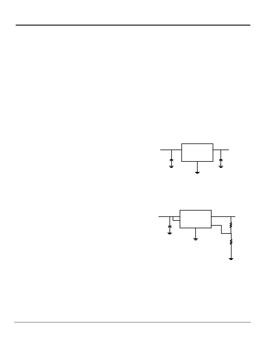
SPX2730
Fig.1 Basic Fixed Output Regulator
V
OUT
V
IN
SPX2732/33
Fig. 2 Adjustable Output Voltage Regulator
V
OUT
V
IN
1
2
3
4
5
R
2
R
1
For best results, the total series resistance should be
small enough to pass the minimum regulator load current
V
OUT
= V
REF
X [ 1 + (R
1
/R
2
) ]
Rev. 12/7/00
SPX2730/31/32/33
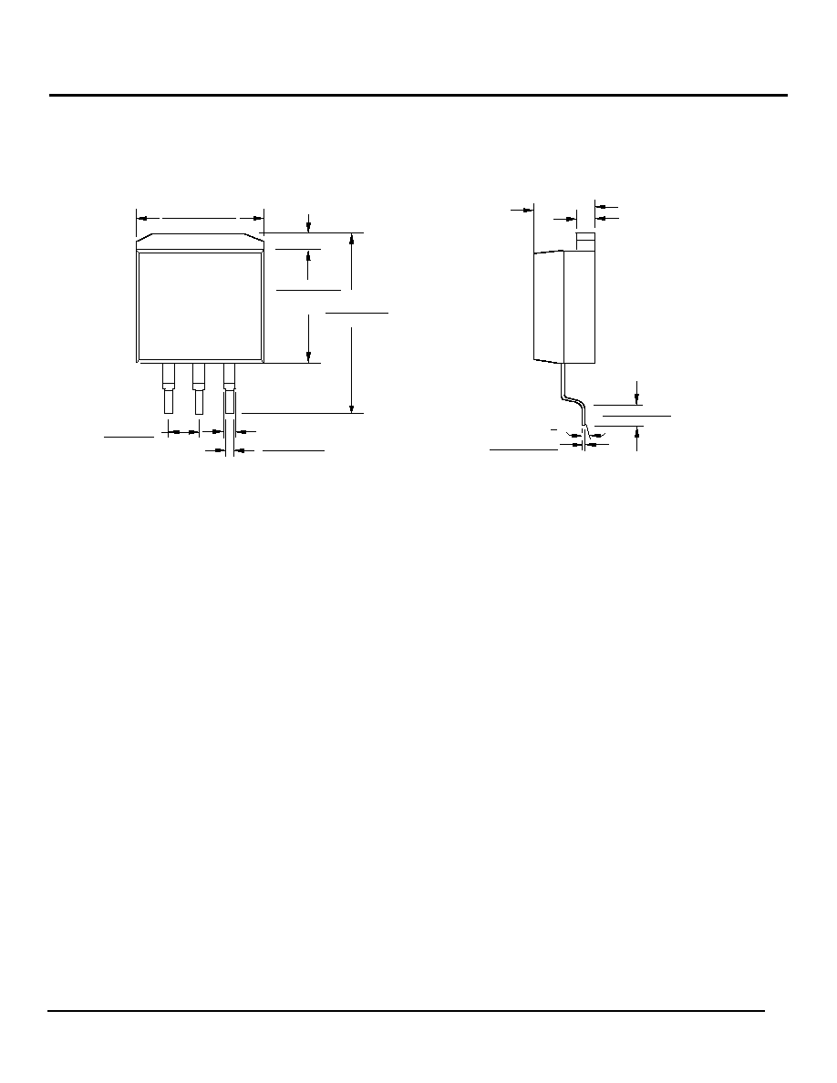
PACKAGE DRAWING
TO-263-3L (T)
0.103 BSC
0.050 (1.270)
0.600
+-
0.025
0.405
0.005
0.055 (1.397)
(10.287
0.127)
±
±
0.356
0.005
(9.042
0.127)
±
±
(15.24 0.635)
±
(2.616)
0.032
+-
0.001
(0.813 0.025)
+-
0.176 0.005
0.050 0.002
0.015
+-
0.003
0∞ 8∞
(0.381
0.074)
+-
0.100
0.010
(2.540
0.254)
±
±
(4.470 0.127)
±
(1.270
0.051)
±
±
±
Rev. 12/7/00
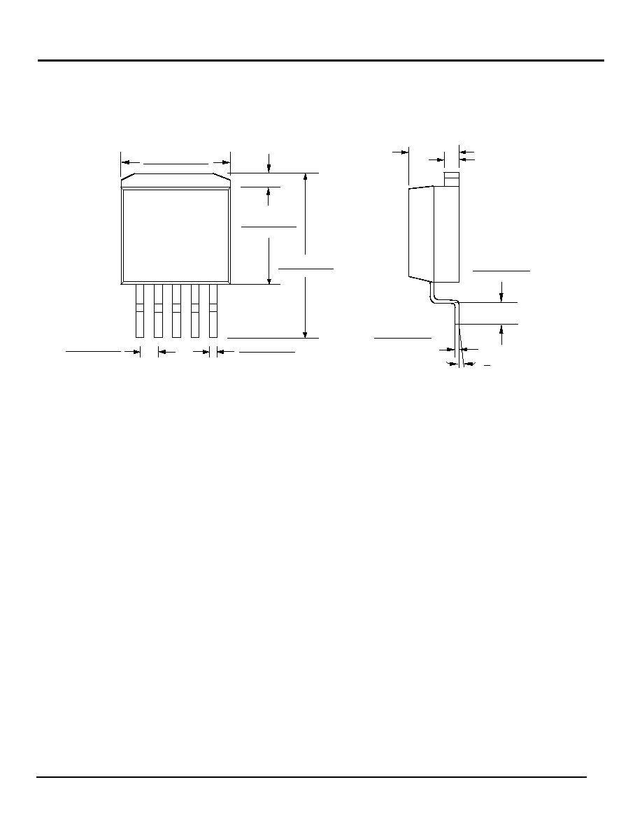
SPX2730/31/32/33
PACKAGE DRAWING
TO-263-5L (T)
0.405
0.005
0.055 (1.397)
0.356
0.005
±
(10.287 ± 0.127)
±
(9.042
0.127)
±
(15.24
0.635)
±
0.600
0.025
±
(1.702
0.127)
±
0.067
0.005
±
(0.813
0.076)
±
0.032
0.003
±
0.176
0.005
±
(4.470
0.127)
±
0.050
0.002
±
(1.270
0.051)
±
0.015 +- 0.003
0∞ 8∞
(0.381
0.074)
+-
0.100
0.010
(2.540
0.254)
±
±
Rev. 12/7/00
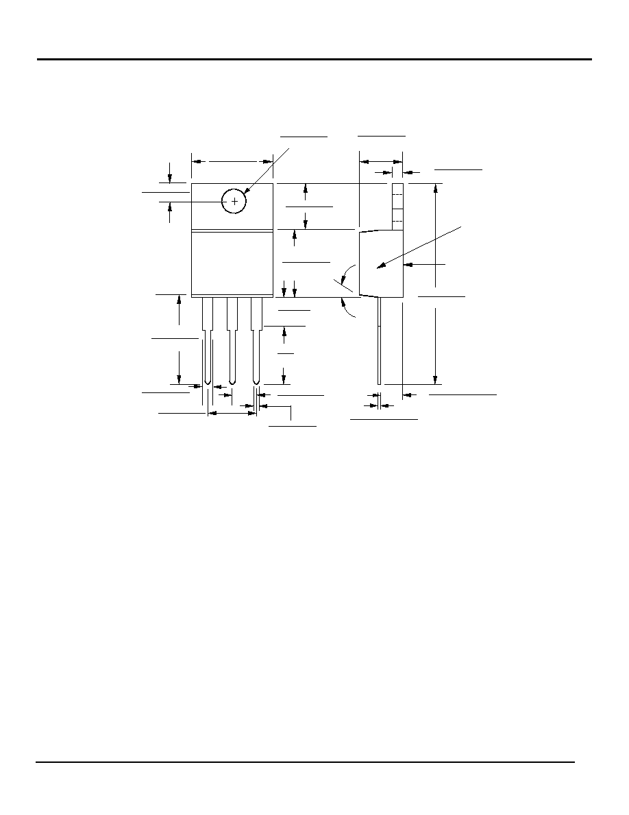
SPX2730/31/32/33
PACKAGE DRAWING
TO-220-3L (U)
0.408 ± 0.013
(10.36 ± 0.33)
0.110 ± 0.010
(2.794 ± 0.254)
0.250 ± 0.010
(6.350 ± 0.254)
0.151D ± 0.002
(3.835 D ± 0.051)
0.180 ± 0.005
(4.572 ± 0.127)
0.050 ± 0.002
(1.270 ± 0.051)
0.340 ± 0.010
(8.636 ± 0.254)
0.150 MIN
(3.81 MIN)
0.410
(10.41)
0.100 ± 0.010
(2.540 ± 0.254)
0.032 ± 0.005
(0.813 ± 0.127)
0.540 ± 0.015
(13.720 ± 0.381)
0.050 TYP
(1.27 TYP)
0.200 ± 0.010
(5.080 ± 0.254)
0.015 ± 0.010/-0.002
(0.381± 0.254/-0.051)
0.015 ± 0.010/-0.015
(2.667± 0.254/-0.381)
1.020 ± 0.015
(25.910 ± 0.381)
SEATING PLANE
Tapered 1
o
2 Sides
7
o
Typ.
Rev. 12/7/00
SPX2730/31/32/33
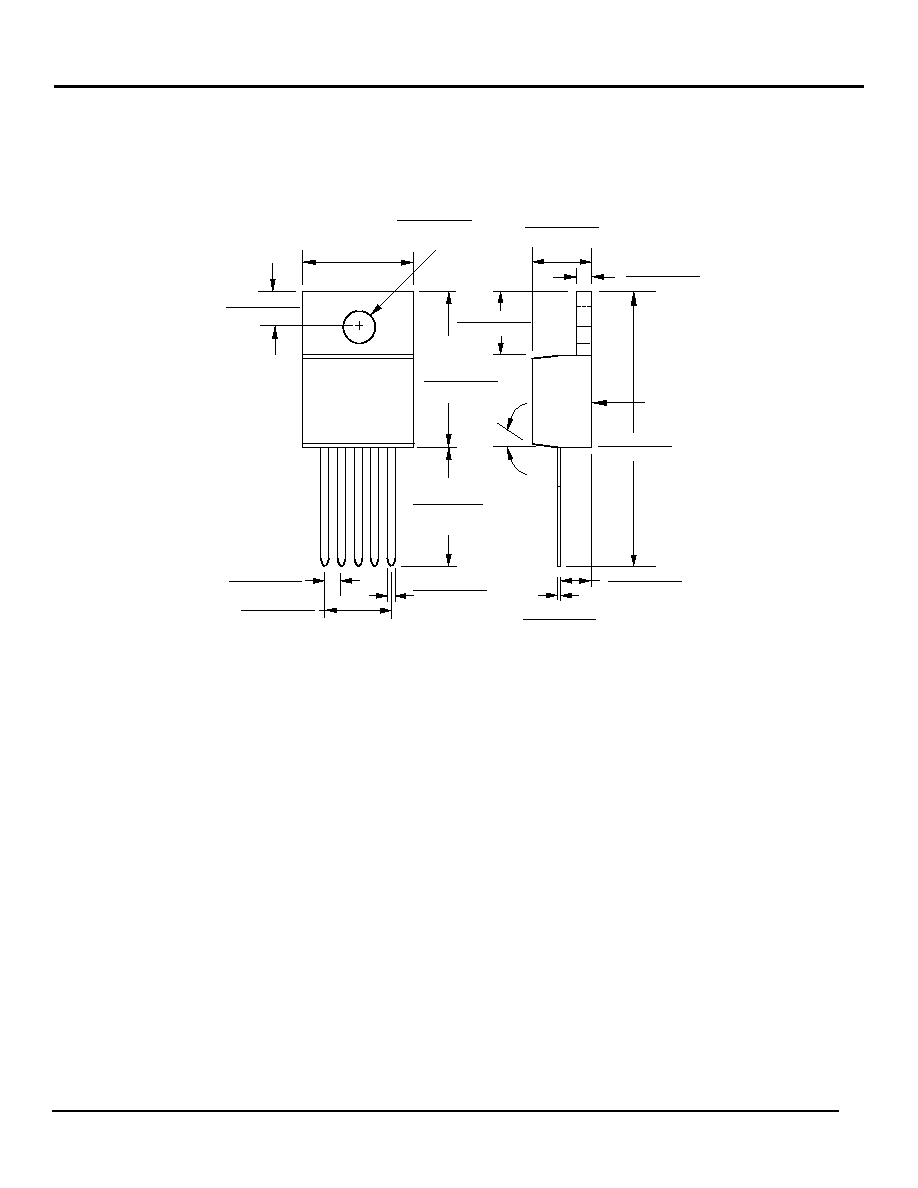
PACKAGE DRAWING
TO-220-5L (U)
0.108 +- 0.005
(2.74 +- 2.74)
0.400 +-0.005
(10.16+- 0.13)
0.150 D+-0.005
(3.81D +-0.13)
0.175 +- 0.005
(4.45 +- 0.13)
0.050 +- 0.005
(1.27 +- 0.13)
0.250 +- 0.005
(6.35 +- 0.13)
0.590 +- 0.005
(14.99 +- 0.13)
SEATING
PLANE
0.547 +- 0.005
(13.89 +- 0.005)
0.067 +- 0.005
(1.70 +- 0.127)
0.268 REF
(6.81 REF)
0.268 REF
0.032 +- 0.005
(0.81 +- 0.13)
0.015 +- 0.005
(0.38 +- 0.13)
0.105 +- 0.005
(2.67 +- 0.13)
1.137 REF
(28.88 REF)
7∞
Typ.
Rev. 12/7/00
SPX2730/31/32/33
ORDERING INFORMATION
Ordering No. Output Voltages
Packages
SPX2730U-3.3
3.3V
3 Lead TO-220
SPX2730U-5.0
5.0V
3 Lead TO-220
SPX2730T-3.3
3.3V
3 Lead TO-263
SPX2730T-5.0
5.0V
3 Lead TO-263
SPX2731U-3.3
3.3V
3 Lead TO-220
SPX2731U-5.0
5.0V
3 Lead TO-220
SPX2731T-3.3
3.3V
3 Lead TO-263
SPX2731T-5.0
5.0V
3 Lead TO-263
SPX2732U
Adj
5 Lead TO-220
SPX2732U-3.3
3.3V
3 Lead TO-220
SPX2732U-5.0
5.0V
3 Lead TO-220
SPX2732T
Adj
5 Lead TO-263
SPX2732T-3.3
3.3V
3 Lead TO-263
SPX2732T-5.0
5.0V
3 Lead TO-263
SPX2733U
Adj
5 Lead TO-220
SPX2733U-3.3
3.3V
3 Lead TO-220
SPX2733U-5.0
5.0V
3 Lead TO-220
SPX2733T
Adj
5 Lead TO-263
SPX2733T-3.3
3.3V
3 Lead TO-263
SPX2733T-5.0
5.0V
3 Lead TO-263
SIGNAL PROCESSING EXCELLENCE
Sipex Corporation
Headquarters and Main Offices:
22 Linnell Circle
Billerica, MA 01821
TEL: (978) 667-8700
FAX: (978) 670-9001
e-mail: sales@sipex.com
233 South Hillview Drive
Milpitas, CA 95035
TEL: (408) 935-7600
FAX: (408) 934-7500
Sipex Corporation reserves the right to make changes to any products described herein. Sipex does not assume any liability arising out of the application or use of any product or circuit described
hereing; neither does it convey any license under its patent rights nor the rights of others.
Corporation