Rev. 10/30/00
SPX2810
1A Low Dropout Voltage Regulator
Adjustable & Fixed Output,
Fast Response
FEATURES
APPLICATIONS
∑ Adjustable Output Down To 1.2V
∑ Portable Palmtop/Notebook Computer
∑ Fixed Output Voltages 1.5V, 2.5V, 3.0V, 3.3V, 5.0V
∑ SMPS Post-Regulator
∑ Output Current Of 1A
∑ Disk Drives
∑ Low Dropout Voltage 1.2V Typ.
∑ Portable Consumer Equipment
∑ Extremely Tight Load And Line Regulation
∑ Portable Instrumentation
∑ Current & Thermal Limiting
∑ Battery charger
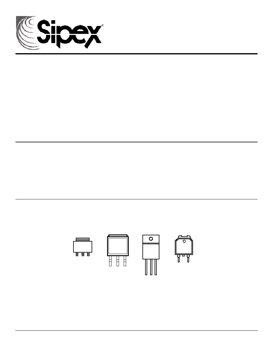
∑ Standard 3-Terminal Low Cost TO-220, TO-263, TO-252 & SOT-223
PRODUCT DESCRIPTION
The SPX2810 is a low power positive voltage regulator designed to source 1A output current. This device is an excellent choice for
use in battery-powered applications and portable computers. The SPX2810 features very low quiescent current and very low dropout
voltage of 1.2V at a full load and lower as output current decreases. This product is available as adjustable or fixed 1.5V, 2.5V, 3.0V,
3.3V, and 5V output voltages.
The SPX2810 is offered in a 3-pin surface mount packages SOT-223, TO-220, TO-252 & DD package. The output capacitor of 10
µF
or larger is needed for the output stability of SPX2810 as required by most other regulator circuits
PIN CONNECTIONS
Front View
TO-220-3 (U)
SPX2810
1
2
3
ADJ/GND V
OUT
V
IN
Top View
TO-263-3 (T)
1
SPX2810
2
3
ADJ/GND V
OUT
V
IN
Front View
TO-252 (R)
ADJ/GND
V
IN
V
OUT
3
2
1
SPX2810
Top View
SOT-223 (M3)
ADJ/ GND V
OUT
V
IN
SPX2810
1
3
2
Rev. 10/30/00
SPX2810
ABSOLUTE MAXIMUM RATINGS
Lead Temp. (Soldering, 10 Seconds) .............................. 300∞C
Input Voltage........................................................ 10V
Storage Temperature Range ............................ -65∞ to +150∞C
Input to Output Voltage Differential .................... 10V
Operating Junction Temperature Range ......................
SPX2810 Control Section.......................... -45∞C +125∞C
SPX2810 Power Transistor.........................-45∞C +150∞C
ELECTRICAL CHARACTERISTICS
(NOTE 1) at I
OUT
= 10mA, T
A
=25
∞C, unless otherwise specified.
PARAMETER CONDITIONS
Typ
SPX2810A
SPX2810
UNITS
Min Max Min Max
1.5V Version
1.485 1.515 1.470 1.530
Output Voltage (Note 2)
SPX2810-1.5V, 0 < I
OUT
< 1A, 3.3V<V
IN
<10V 1.5
1.47 1.53 1.455 1.545
V
2.5V Version
2.475 2.525 2.450 2.550
Output Voltage (Note 2)
SPX2810-2.5V, 0 < I
OUT
< 1A, 4.0V<V
IN
<10V 2.5
2.45 2.55 2.425 2.575
V
2.85V Version
2.822 2.879 2.793 2.907
Output Voltage (Note 2)
SPX2810-2.85V, 0
I
OUT
1A,
4.5V
V
IN
10V
2.85
2.793 2.907 2.650 2.936
V
3.0V Version
2.970 3.030 2.94 3.06
Output Voltage (Note 2)
SPX2810-3.0V, 0
I
OUT
1A, 4.5VV
IN
10V
3
2.940 3.060 2.79 3.09
V
3.3V Version
3.267 3.333 3.234 3.366
Output Voltage (Note 2)
SPX2810-3.3V, 0
I
OUT
1A, 4.8VV
IN
10V
3.3
3.234 3.366 3.069 3.399
V
5.0V Version
4.950 5.050 4.9
5.1
Output Voltage (Note 2)
SPX2810-5.0V, 0
I
OUT
1A, 6.5VV
IN
12V
5
4.900 5.100 4.65 5.15
V
All Voltage Options
1.250
Reference Voltage (V
REF
)
V
IN
7V, P Pmax
1.5V
(V
IN
-V
OUT
)
5.75V, 10mAI
OUT
1A
1.225
1.263
1.270
1.225
1.225
1.212
1.270
1.288
V
Min. Load Current (Note 3)
1.5V
(V
IN
≠V
OUT
)
5.75V
5 10 10
mA
Line Regulation (
V
REF
(V
in
)) 2.75V
V
IN
7V, I
OUT
=10mA, T
J
=25∫C (Note 3)
0.005 0.2 0.2
V
IN
7V, I
OUT
=0mA, T
J
=25∫C (Note 2)
0.005 0.2 0.2
%
10mA
I
OUT
1A, (V
IN
-V
OUT
)=3V, T
J
=25∫C
(Note 3)
0.05 0.3 0.3
Load Regulation(
V
REF
(I
OUT
))
0
I
OUT
1A, V
IN
=7V, T
J
=25∫C (Note 2)
0.05 0.3 0.3
%
Dropout Voltage
V
REF
=1% I
OUT
= 1A (Note 3)
I
OUT
1A (Note 2)
1.1 1.2 1.2
V
IN
=7V
Current Limit
I
OUT
(MAX)
1.4V
(V
IN
- V
OUT
) (Note3)
2 1.2 1.2 A
Rev. 10/30/00
SPX2810
ELECTRICAL CHARACTERISTICS (Cont.)
Long Term Stability
T
A
=125∫C, 1000 Hrs.
0.3
(Note 2)
1 1 %
Thermal Regulation (
V
OUT
(Pwr))
T
A
=25∫C, 20 ms pulse
0.01
0.020
0.020
%/W
Temperature Stability (
V
OUT
(T))
0.25
%
Output Noise, RMS
10Hz to 10kHz T
A
=25∫C 0.003
%
Vo
3.0
3.0
TO-220
Junction to Tab
Junction to Ambient
60
60
3.0
3.0
DD Package
Junction to Tab
Junction to Ambient
60
60
15
15
Thermal Resistance
SOT-223 Package
Junction to Tab
Junction to Ambient
156
156
The Bold specifications apply to the full operating temperature range.
Note 1: Changes in output voltage due to heating effects are covered under the specification for thermal regulation.
Note 2: Fixed Version Only
Note 3: Adjustable Version Only
∫C/W

Rev. 10/30/00
SPX2810
APPLICATION HINTS
The SPX2810 incorporates protection against over-current
faults, reversed load insertion, over temperature operation, and
positive and negative transient voltage. However, the use of
an output capacitor is required in order to improve the stability
and the performances.
Stability
The output capacitor is part of the regulator's frequency
compensation system. Either a 22
µF aluminum electrolytic
capacitor or a 10
µF solid tantalum capacitor between the
output terminal and ground guarantees stable operation for all
operating conditions.
However, in order to minimize overshoot and undershoot, and
therefore optimize the design, please refer to the section
`Ripple Rejection'.
Ripple Rejection
Ripple rejection can be improved by adding a capacitor
between the ADJ pin and ground as shown in figure 6. When
ADJ pin bypassing is used, the value of the output capacitor
required increases to its maximum (22
µF for an aluminum
electrolytic capacitor, or 10
µF for a solid tantalum capacitor).
If the ADJ pin is not bypass, the value of the output capacitor
can be lowered to 10
µF for an electrolytic aluminum capacitor
or 4.7
µF for a solid tantalum capacitor.
However the value of the ADJ-bypass capacitor should be
chosen with respect to the following equation:
C = 1 / ( 6.28 * F
R
* R
1
)
Where C
= value of the capacitor in Farads (select an
equal or larger standard value),
F
R
= ripple frequency in Hz,
R
1
= value of resistor R
1
in Ohms.
If an ADJ-bypass capacitor is use, the amplitude of the output
ripple will be independent of the output voltage. If an ADJ-
bypass capacitor is not used, the output ripple will be
proportional to the ratio of the output voltage to the reference
voltage:
M = V
OUT
/ V
REF
Where M = multiplier for the ripple seen when the ADJ pin
is optimally bypassed.
V
REF
= Reference Voltage
Reducing parasitic resistance and inductance
One solution to minimize parasitic resistance and inductance is
to connect in parallel capacitors. This arrangement will
improve the transient response of the power supply if your
system requires rapidly changing current load condition.
Thermal Consideration
Although the SPX2810 offers some limiting circuitry for
overload conditions, it is necessary not to exceed the
maximum junction temperature, and therefore to be careful
about thermal resistance. The heat flow will follow the lowest
resistance path, which is the Junction-to-case thermal
resistance. In order to insure the best thermal flow of the
component, a proper mounting is required. Note that the case
of the device is electrically connected to the output. In case
the case has to be electrically isolated, a thermally conductive
spacer can be used. However do not forget to consider its
contribution to thermal resistance.
Assuming:
V
IN
= 10V, V
OUT
= 5V, I
OUT
= 1.5A, T
A
= 50
∞C/W,
Heatsink Case
= 6
∞C/W,
Heatsink Case
= 0.5
∞C/W,
JC
= 3
∞C/W
Power dissipation under this condition
P
D
= (V
IN
≠ V
OUT
) * I
OUT
= 7.5W
Junction Temperature
T
J
= T
A
+ P
D
* (
Case - HS
+
HS
+
JC
)
For the Control Sections
T
J
= 50 + 7.5*(0.5+6=3) = 121.25
∞C
121.25
∞C < T
J (max)
for the Control & Power Sections.
In both case reliable operation is insured by adequate junction
temperature.
Rev. 10/30/00
SPX2810
Basic Adjustable Regulator
Output Voltage
Consider Figure 2. The resistance R
1
generates a constant
current flow, normally the specified load current of 10mA.
This current will go through the resistance R
2
to set the overall
output voltage. The current I
ADJ
is very small and constant.
Therefore its contribution to the overall output voltage is very
small and can generally be ignored.
Load Regulation
Parasitic line resistance can degrade load regulation. In order
not to affect the behavior of the regulator, it is best to connect
directly the R
1
resistance from the resistor divider to the case,
and not to the load. For the same reason, it is best to connect
the resistor R
2
to the Negative side of the load.
Output Voltage
The fixed voltage LDO voltage regulator are simple to use
regulators since the V
OUT
is preset to the specifications. It is
important however, to provide the proper output capacitance
for stability and improvement. For most operating conditions
a capacitance of 22uF tantalum or 100uF electrolytic will
ensure stability and prevent oscillation.
SPX2810
Fig.2 Basic Adjustable Regulator
V
IN
V
REF
V
OUT
= V
REF
* ( 1 + R
2
/R
1
) + I
ADJ
* R
2
I
ADJ
50µA
V
OUT
R
2
R
1
SPX2810
Fig.3 Basic Adjustable Regulator
V
IN
R
2
R
1
Connect R
2
to Load
R
L
Connect R
1
to
Case of Regulator
R
P
Parasitic Line
Resistance
SPX2810
Basic Fixed Regulator
V
IN
V
OUT
5V
C1
10uF
C2
10uF
3.3V