1
Date: 5/17/04 SPX2815 1.5A Low Dropout Voltage Regulator
© Copyright 2004 Sipex Corporation
1.5A Low Dropout Voltage Regulator
SPX2815
DESCRIPTION
FEATURES
Guaranteed 1.5A Output Current
Three Terminal Adjustable or Fixed
2.5V, 3.3V and 5.0V
Low Quiescent Current
Low Dropout Voltage of 1.1V at 1.5A
0.1% Line and 0.1% Load Regulation
Stable with 10uF Ceramic Capacitor
Overcurrent and Thermal Protection
Available Packages: TO-252,
TO-220, and TO-263
Similar to Industry Standard LT1086/
LT1586
Æ
The SPX2815 is a low power positive-voltage regulator designed to satisfy moderate power
requirements with a cost effective, small footprint solution. This device is an excellent choice for
use in battery-powered applications and portable computers. The SPX2815 features very low
quiescent current and a low dropout voltage of 1.1V at a full load. As output current decreases,
quiescent current flows into the load, increasing efficiency. SPX2815 is available in adjustable
or fixed 2.5V, 3.3V and 5.0V output voltages.
The SPX2815 is offered in several 3-pin surface mount packages: TO-252, TO-220 and TO-263.
An output capacitor of 10
µ
F ceramic or tantalum provides unconditional stability.
APPLICATIONS
Desktop PC's Servers
Powering VGA and Sound Cards
Cordless Phones
Battery Chargers
Adjustable Power Supplies
Portable Instrumentation
SMPS Post-Regulator
Constant Current Regulators
Disk Drives
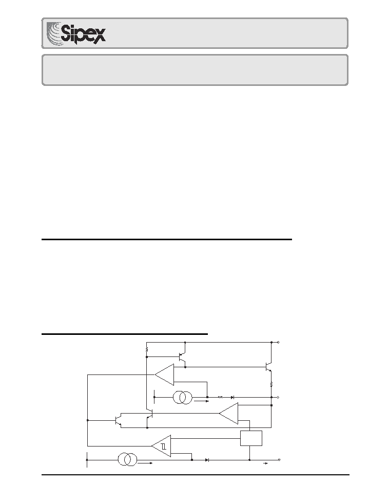
FUNCTIONAL DIAGRAM (Adjustable)
+
-
Current Limit
I
CL
I
TL
Thermal Limit
V
REF
AMP
V
OUT
V
IN
ADJ/GND
+
≠
I
ADJ
~ 50µA
≠
1.25V
_
+
Refer to Page 5 for Pinouts

2
Date: 5/17/04 SPX2815 1.5A Low Dropout Voltage Regulator
© Copyright 2004 Sipex Corporation
Power Dissipation.......................................Internally Limited
Lead Temperature (soldering, 5 seconds) ...............260
∞
C
Storage Temperature Range.......................-65
∞
C to +150
∞
C
Operating Junction Temperature Range.....-40
∞
C to +125
∞
C
Input Supply Voltage .................................................... +10V
Input to Output Voltage ................................................ +8.8V
ESD Rating .............................................................. 2kV min
PARAMETER
MIN
TYP
MAX
MIN
TYP MAX UNITS
CONDITIONS
2.5V Version
SPX2815A
SPX2815
Output Voltage
2.475 2.500
2.525 2.450 2.500
2.550
V
I
OUT
= 10mA, V
IN
=4.5V
2.450
2.550 2.425
2.575
10mA
I
OUT
3A, 4.25V
V
IN
10V
3.30V Version
Output Voltage
3.267 3.300
3.333 3.234 3.300
3.366
V
I
OUT
= 10mA, V
IN
=5V
3.234
3.366 3.201
3.399
10mA
I
OUT
3A, 4.75V
V
IN
10V
5.0V Version
Output Voltage
4.950 5.000
5.050 4.900 5.000
5.100
V
I
OUT
=10mA, V
IN
=7V
4.900
5.100 4.850
5.150
10mA
I
OUT
3A, 6.50V
V
IN
10V
All Voltage Options
Reference Voltage
1.238 1.250
1.262 1.225 1.250
1.275
V
I
OUT
=10mA, (V
IN
- V
OUT
)= 2V
1.225
1.275 1.212
1.287
10mA
I
OUT
3A, 1.5V
(V
IN
-V
OUT
)
10V
Output Voltage
0.3
0.5
%
Temperature Stability
Line Regulation
0.1
0.2
0.1
0.2
%
4.25V
V
IN
10V,V
OUT
=2.5V,I
OUT
=10mA
0.1
0.2
0.1
0.2
4.75V
V
IN
10V,V
OUT
=3.3V,I
OUT
=10mA
0.1
0.2
0.1
0.2
6.50V
V
IN
10V,V
OUT
=5.0V,I
OUT
=10mA
Load Regulation
0.1
0.3
0.1
0.3
%
10mA
I
OUT
1.5A, V
OUT
=2.5V
0.1
0.3
0.1
0.3
10mA
I
OUT
1.5A, V
OUT
=3.3V
0.1
0.3
0.1
0.3
10mA
I
OUT
1.5A, V
OUT
=5.0V
Dropout Voltage
1.00
1.00
V
I
OUT
=0.5A
(Note 2)
1.10
1.2
1.10
1.2
I
OUT
=1.5A
Quiescent Current
4
10
4
10
mA
Fixed voltage versions
Adjust Pin Current
50
120
50
120
µ
A
Current Limit
2.5
2.5
A
(V
IN
-V
OUT
)=5V
Thermal Regulation
0.01
0.1
0.01
0.1
%/W
25
∞
C, 30mS pulse
Ripple Rejection
60
75
60
75
dB
f
RIPPLE
=120Hz, (V
IN
-V
OUT
)=2V,
V
RIPPLE
=1V
PP
Long Term Stability
0.03
0.03
%
125
∞
C, 1000Hrs
RMS Output Noise
0.003
0.003
%
% of V
OUT
, 10Hz
f
10kHz
ELECTRICAL CHARACTERISTICS
at V
IN
=V
OUT
+ 1.5V, T
A
= 25
∞C, C
IN
= C
OUT
= 10
µF, I
OUT
=10mA, unless otherwise specified. The Boldface applies over the
full operating temperature range.
ABSOLUTE MAXIMUM RATINGS
3
Date: 5/17/04 SPX2815 1.5A Low Dropout Voltage Regulator
© Copyright 2004 Sipex Corporation
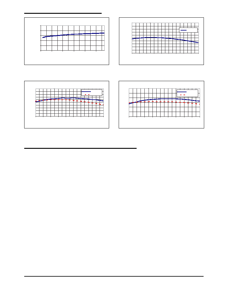
TYPICAL PERFORMANCE CHARACTERISTICS
Figure 1. Line Regulation for SPX2815U-3.3; I
OUT
=10mA
3.300
3.305
3.310
3.315
3.320
3.325
4.5
6.5
8.5
10.5
12.5
14.5
Vin (V)
V
out (V)
1.225
1.23
1.235
1.24
1.245
1.25
1.255
1.26
1.265
1.27
1.275
-50
-30
-10
10
30
50
70
90
110
130
Temp (C)
V
out (V)
1.25v Adj
Figure 2. V
OUT
vs Temperature, V
IN
=2.5V, I
OUT
=10mA
Figure 3. V
IN
=4.0V, I
OUT
=10mA
2.45
2.46
2.47
2.48
2.49
2.5
2.51
2.52
2.53
2.54
2.55
-50
-30
-10
10
30
50
70
90
110
130
Temp (C)
V
out (V)
2.5v Adj
2.5v Fixed
Figure 4. V
IN
=5.0V, I
OUT
=10mA
3.26
3.28
3.3
3.32
3.34
3.36
3.38
-50
-30
-10
10
30
50
70
90
110
130
Temp (C)
V
out (V)
3.3v Adj
3.3v Fixed
Output Capacitor
To ensure the stability of the SPX2815, an
output capacitor of at least 10
µF (ceramic or
tantalum) or 22
µF (aluminum) is required. The
value may change based on the application
requirements of the output load or temperature
range. The value of ESR can vary based on the
type of capacitor used in the applications to
guarantee stability. The recommended value
for ESR is 0.5
or less. A larger value of output
capacitance (up to 100
µF) can improve the load
transient response.
Soldering Methods
The SPX2815 die is attached to the heatsink lead
which exits opposite the input, output, and ground
pins.
Thermal Characteristics
The SPX2815 features the internal thermal lim-
iting to protect the device during overload con-
ditions. Special care needs to be taken during
continuous load conditions such that the maxi-
mum junction temperature does not exceed
125
∞C. Thermal protection is activated at >179∞C
and deactiviated at <165
∞C.
The thermal interaction from other components
in the application can effect the thermal resis-
tance of the SPX2815. The actual thermal
resistance can be determined with experimenta-
tion.
SPX2815 power dissipation is calculated as
follows:
P
D
= (V
IN
- V
OUT
)(I
OUT
)
Maximum Junction Temperature range:
T
J
= T
A
(max) + P
D
* thermal resistance
(junction-to-ambient)
Maximum junction temperature must not ex-
ceed the 125
∞C.
APPLICATION INFORMATION
4
Date: 5/17/04 SPX2815 1.5A Low Dropout Voltage Regulator
© Copyright 2004 Sipex Corporation
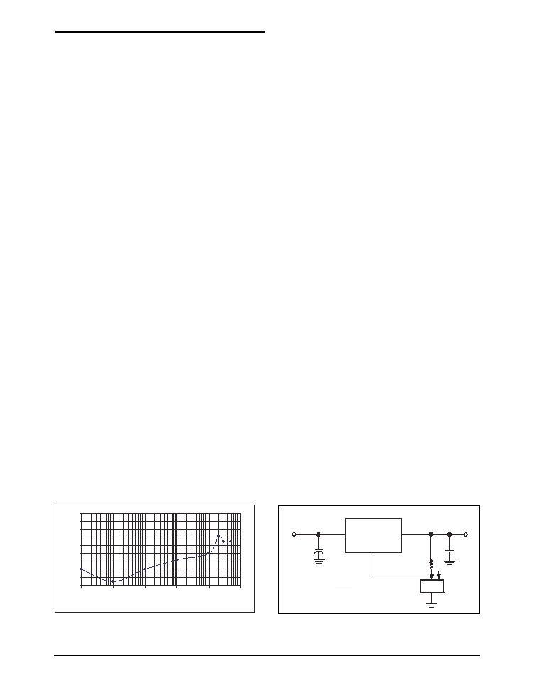
-90
-80
-70
-60
-50
-40
-30
-20
-10
0
10
100
1000
10000
100000
1000000
Frequency, Hz
Ripple Rejection, Db
Figure 5. Ripple Rejection; Vin=3.3V, Vout=1.8V (adj.),
Iload=200mA
Figure 6. Current Source
LOAD
ADJ
SPX2815
V
IN
C
1
OUT
IN
4.7
µ
F
C
2
I
OUT
R
1
V
REF
R
1
I
OUT
=
+
V
OUT
Ripple Rejection
Ripple rejection can be improved by adding a
capacitor between the ADJ pin and ground as
shown in Figure 8. When ADJ pin bypassing
is used, the value of the output capacitor
required increases to its maximum. If the ADJ
pin is not bypassed, the value of the output
capacitor can be lowered to 22
µF for an
electrolytic aluminum capacitor or 10
µF for a
solid tantalum capacitor (Fig 7).
However the value of the ADJ-bypass capaci-
tor should be chosen with respect to the
following equation:
C = 1 / ( 6.28 * F
R
* R
1
)
Where
C = value of the capacitor in Farads
(select an equal or larger standard value),
F
R
= ripple frequency in Hz,
R
1
= value of resistor R1 in Ohms.
If an ADJ-bypass capacitor is used, the
amplitude of the output ripple will be indepen-
dent of the output voltage. If an ADJ-bypass
capacitor is not used, the output ripple will be
proportional to the ratio of the output voltage
to the reference voltage:
M = V
OUT
/ V
REF
Where M = multiplier for the ripple seen when
the ADJ pin is optimally bypassed.
V
REF
=1.25V
Ripple rejection for the adjustable version is
shown in Figure 5.
Output Voltage
The output of the adjustable regulator can be
set to any voltage between 1.25V and 15V.
The value of V
OUT
can be quickly approxi-
mated using the formula
V
OUT
=1.25 *(R
1
+ R
2
)/R
1
A small correction to this formula is required
depending on the values of resistors R
1
and R
2
,
since the adjustable pin current (approx
50
µA) flows through R
2
. When I
ADJ
is taken
into account, the formula becomes
V
OUT
= V
REF
(1+ (R
2
/R
1
)) + I
ADJ
* R
2
where
V
REF
=1.25V
Layout Considerations
Parasitic line resistance can degrade load
regulation. In order to avoid this, connect R
1
directly to V
OUT
as illustrated in Figure 13.
For the same reason, R
2
should be connected
to the negative side of the load.
APPLICATION INFORMATION: Continued
5
Date: 5/17/04 SPX2815 1.5A Low Dropout Voltage Regulator
© Copyright 2004 Sipex Corporation
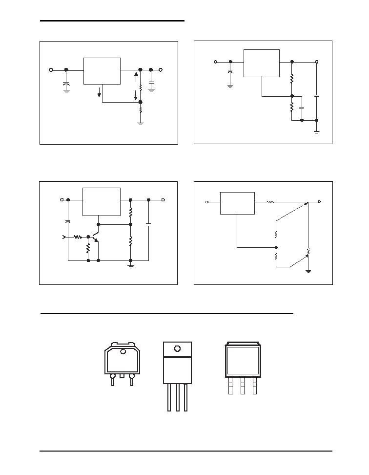
Figure 9. 5V Regulator with Shutdown
SPX2815
V
IN
R
1
R
2
10
µ
F
10
µ
F*
1k
,
330
1%
+
+
4.7
µ
F
C
1
*C
1
improves ripple rejection.
Z
C
should be ~ R1 at ripple frequency
5V
ADJ
IN
OUT
(Note A)
V
OUT
Note A: V
IN(MIN)
= (Intended V
OUT
) + (V
DROPOUT (MAX)
)
1%
1k
SPX2815
10
µ
F
1%
330W
1%
+
+
4.7
µ
F
5V
ADJ
IN
OUT
(Note A)
1K
1k
TTL
Input
2N3904
DROPOUT (MAX)
Note A: V
IN(MIN)
= (Intended V
OUT
) + (V
)
V
IN
Figure 10. Recommended Connections for Best Results
Figure 8. Improving Ripple Rejection
SPX2815
R
2
R
1
Connect R
2
to Load
R
L
Connect R to
Case of Regulator
R
P
Parasitic Line
Resistance
ADJ
V
OUT
V
IN
IN
OUT
I
ADJ
SPX2815
C
1
R
1
R
2
V
OUT
V
IN
C
2
V
OUT
= V
REF
(1+R
2
/R
1
) +I
ADJ
R
2
V
REF
50
µ
A
ADJ
4.7
µ
F +
Figure 7. Typical Adjustable Regulator
APPLICATION INFORMATION: Continued
Top View
TO-263-3 (T)
1
2
3
Front View
TO-220-3 (U)
1
2
3
Front View
TO-252 (R)
ADJ/GND
V
OUT
1
2
3
V
IN
ADJ/GND
V
OUT
V
IN
ADJ/GND
V
OUT
V
IN
PINOUTS