 | –≠–ª–µ–∫—Ç—Ä–æ–Ω–Ω—ã–π –∫–æ–º–ø–æ–Ω–µ–Ω—Ç: SPX2947T5 | –°–∫–∞—á–∞—Ç—å:  PDF PDF  ZIP ZIP |
1
Rev. B Date:01/20/04
SPX2945 400mA Low Dropout Voltage Regulator with Shutdown
©Copyright 2004 Sipex Corporation
SPX2945
DESCRIPTION
FEATURES
Output 3.3V, 5.0V at 400mA Output
Very Low Quiescent Current, 100
µ
A
Low Dropout Voltage, 420mV at 400mA
Extremely Tight Load and Line Regulation
Very Low Temperature Coefficient
Current & Thermal Limiting
Error Flag Warns Of Output Dropout
Logic-Controlled Electronic Shutdown
Output Programmable From 1.24V to 20V
(for SO-8)
Æ
The SPX2945 is a low power voltage regulator. This device is an excellent choice for use in battery-powered
applications such as cordless telephones, radio control systems, and portable computers. The SPX2945
features very low quiescent current (100
µ
A Typ.) and very low dropout voltage. This includes a tight initial
tolerance of 1% max and very low output temperature coefficient, making the SPX2945 useful as a low-
power voltage reference.
The error flag output feature is used as power-on reset for warning of a low output voltage, due to a falling
voltage input of batteries. Another feature is the logic-compatible shutdown input which enables the
regulator to be switched on and off. The SPX2945 is offered in 3-pin TO-220 package, SO-8 (same pin
out as SPX2951), SOT-223, surface mount 3-Pin TO-252, 3-Pin TO-263 packages and 5-Pin TO-263.
The regulator output voltage (of the 8-pin SO-8) may be pin-strapped for a 3.3V and 5.0V or programmed
from 1.24V to 20V with an external pair of resistors. Look for SPX2951 for 150mA and SPX2954 for 250mA
applications.
400mA Low Dropout Voltage Regulator with Shutdown
TO-220-3 (U)
1
2
3
V
IN
V
OU
GN
SPX2945
1
3
2
5
4
SPX2945
5 Pin TO-263
Er
V
IN
GND
V
OUT
SD
1
3
2
SOT-223 (M3)
V
IN
GN
V
OU
SPX2945
2
1
3
4
8
7
6
5
8-Pin Surface Mount
V
OU
SENS
SHUTDOWN
GN
V
IN
FEEDBACK
5V/ 3.3V TAP
ERRO
SPX2945
TO-252 (R)
1
2
3
V
IN
V
OU
GN
SPX2945
TO-263-5
V
IN
TO-263-3 (T)
V
OU
GN
SPX2945
3
2
1
(S)
(T5)
100K
ERROR
______
SD
V
OUT
GND
FB
+V
IN
0.01
µ
F
3
8
1
4
7
SHUTDOWN
INPUT
SPX2945
OFF
ON
+V
IN
5
10
µ
F
V
REF
R
2
R
1
+
ERROR
OUTPUT
1.2V to 20V
+
2.2
µ
F
+
SPX2945
V
IN
5V
IN
GND
OUT
0.1
µ
F
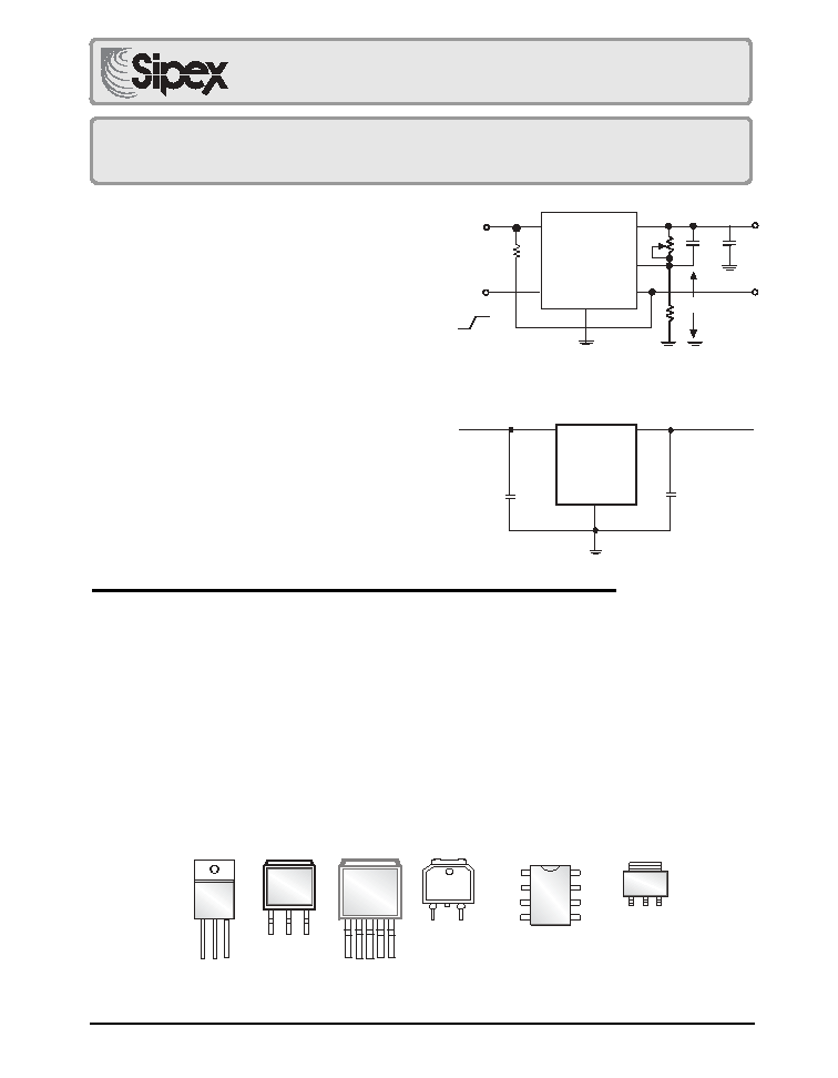
Adjustable Regulator
5V Regulator Circuit
2
Rev. B Date:01/20/04
SPX2945 400mA Low Dropout Voltage Regulator with Shutdown
©Copyright 2004 Sipex Corporation
ELECTRICAL CHARACTERISTICS
Electrical characteristics at V
IN
= V
O
+1V, I
O
= 1mA, C
OUT
= 2.2
µF, T
A
= 25
∞C, unless otherwise specified. The denotes
the specifications wich apply over full operating tempeture range -40
∞C to +85∞C, unless noted.
PARAMETER
CONDITIONS MIN TYP MAX
UNITS
(Note 2)
3.3V Version
Output Voltage
3.267 3.3 3.333 V
1mA
I
L
400mA 3.217 3.3 3.382
5.0V Version
Output Voltage
4.950 5.0 5.050 V
1mA
I
L
400mA 4.880 5.0 5.120
All Voltage Options
Output Voltage
20
100
ppm/
∞
C
Temperature Coefficient (Note1)
Line Regulation (Note 3) 6V
V
IN
20V (Note 4)
1.5
20
mV
Load Regulation (Note 3) I
L
=1 to 400mA 6
20 mV
30
Dropout Voltage (Note5) I
L
=1mA
60
100 mV
150
I
L
=400mA
360 450
700
Ground Current I
L
=1mA
100 200
µ
A
300
I
L
=150mA
2
4 mA
6
I
L
=300mA
4
8
12
I
L
=400mA
8
15
25
Current Limit V
OUT
=0
330
800
mA
Thermal Regulation
0.05 0.2 %/W
Output Noise,
10Hz to 100kHz,
C
L
=2.2
µ
F
400
µ
V
RMS
I
L
=100mA C
L
=33
µ
F
260
PSRR at 100KHz
31
dB
I
L
=100mA C
L
=10
µ
F
Adjustable 8 Pin Version only
Reference Voltage
1.210 1.235 1.260 V
Reference Voltage Over Temperature 1.185 1.285 V
Feedback Pin Bias Current
20
40 nA
60
Reference Voltage Temp.
20
ppm/
∞
C
Coefficient
Power Dissipation ........................................................ Internally Limited
Lead Temp. (Soldering, 5 Seconds) ............................................. 260
∞
C
Storage Temperature Range ........................................ -65
∞
C to +150
∞
C
Operating Junction Temperature Range ....................... -40
∞
C to +125
∞
C
Input Supply Voltage ......................................................... -20V to +26V
ABSOLUTE MAXIMUM RATINGS
Feedback Input Voltage ................................................ -1.5V to +26V
Shutdown Input Voltage ................................................ -0.3V to +26V
Error Comparator Output .............................................. -0.3V to +26V
ESD Rating ............................................................................ 2kV Min
3
Rev. B Date:01/20/04
SPX2945 400mA Low Dropout Voltage Regulator with Shutdown
©Copyright 2004 Sipex Corporation
PARAMETER CONDITIONS MIN TYP
MAX
UNITS
(Note 2)
Feedback Pin Bieas Current
0.1
nA/
∞
C
Temperature Coefficient
Output Leakage Current
V
0H
=20V
0.01
1
µ
A
2
Output Low Voltage
V
IN
=4.5V
150
250 mV
I
0L
=400
µ
A
400
Upper Threshold Voltage
(Note 6) 40 60
mV
25
Lower Threshold Voltage
(Note 6)
75
95 mV
140
Hysteresis
(Note 6)
15
mV
Input Logic Voltage
Low (Regulator ON)
0.7
V
High (Regulator OFF)
1.3
2.0
Shutdown Pin Input Current
VS=2.4V
30
50
µ
A
100
VS=26V
450
600
750
Regulator Output Current
(Note 7) 10 3
µ
A
in Shutdown
20
ELECTRICAL CHARACTERISTICS: Continued
Electrical characteristics at V
IN
= V
O
+1V, I
O
= 1mA, C
OUT
= 2.2
µF, T
A
= 25
∞C, unless otherwise specified. applies over the
full operating temperature range.
Note 1: Output or reference voltage temperature coefficients defined as the worst case voltage change divided by
the total temperature range.
Note 2: Unless otherwise specified all limits are guaranteed for T
j
= 25
∞
C, V
IN
= 6V, I
L
= 1mA and C
L
= 2.2
µ
F. Additional
conditions for the 8-pin versions are feedback tied to 5V/3.3V tap and output tied to output sense (V
OUT
= 5V) and
V
SHUTDOWN
0.8V.
Note 3: Regulation is measured at constant junction temperature, using pulse testing with a low duty cycle. Changes
in output voltage due to heating effects are covered under the specification for thermal regulation.
Note 4: Line regulation for the SPX2945 is tested at 150
∞
C for I
L
= 1 mA. For T
J
= 125
∞
C, line regulation is guaranteed
by design.
Note 5: Dropout voltage is defined as the input to output differential at which the output voltage drops 100 mV below
its nominal value measured at 1V differential at very low values of programmed output voltage, the minimum input
supply voltage of 2V ( 2.3V over temperature) must be taken into account.
Note 6: Comparator thresholds are expressed in terms of a voltage differential at the feedback terminal below the
nominal reference voltage measured at 6V input. To express these thresholds in terms of output voltage change,
multiply by the error amplifier gain = V
OUT
/V
REF
= (R1 + R2)/R2. For example, at a programmed output voltage of 5V,
the Error output is guaranteed to go low when the output drops by 95 mV x 5V/1.235 = 384 mV. Thresholds remain
constant as a percent of V
OUT
as V
OUT
is varied, with the dropout warning occurring at typically 5% below nominal, 7.5%
guaranteed.
Note 7: V
SHUTDOWN
2V, V
IN
26V, V
OUT
= 0, Feedback pin tied to 5V/3.3V Tap.

4
Rev. B Date:01/20/04
SPX2945 400mA Low Dropout Voltage Regulator with Shutdown
©Copyright 2004 Sipex Corporation
SPX2945 - 5.0V BLOCK DIAGRAM
FEEDBACK
INPUT
OUTPUT
UNREGULATED DC
SHUTDOWN
GROUND
ERROR
______
5V TAP
SENSE
5V at 400mA
MAX
TO CMOS OR
TTL
REFERENCE
ERROR DETECTION
COMPARATOR
ERROR
AMPLIFIER
1.23V
FROM
CMOS OR
TTL
+
+
+
+
+
+
60 mV
3
7
8
1
2
6
5
4
.
60k
330k
180k
.
.
1
µ
F
_
_
External Capacitors
The stability of the SPX2945 requires a 2.2
µF or
greater capacitor between output and ground.
Oscillation could occur without this capacitor.
Most types of tantalum or aluminum electrolytic
works fine here. For operations of below -25
∞C
solid tantalum is recommended since the many
aluminum types have electrolytes that freeze at
about -30
∞C. The ESR of about 5 or less and
resonant frequency above 500kHz are the most
important parameters in the value of the capaci-
tor. The capacitor value can be increased with-
out limit.
At lower values of output current, less output
capacitance is required for stability. For the
currents below 10mA the value of the capacitor
can be reduced to 0.5
µF and 0.15µF for 1mA.
More output capacitance needed for the 8-pin
version at voltages below 5V since it runs the
error amplifier at lower gain. At worst case
4.7
µF or greater must be used for the condition
of 250mA load at 1.23V output.
The SPX2945, unlike other low dropout regu-
lators will remain stable and in regulation with
no load in addition to the internal voltage di-
vider. This feature is especially important in
applications like CMOS RAM keep-alive.
If there is more than 10 inches of wire between
the input and the AC filter capacitor, or if a
battery is used as the input, then a 0.1
µF tanta-
lum or aluminum electrolytic capacitor should
be placed from the input to the ground.
Instability can occur if there is stray capaci-
tance to the SPX2945 feedback terminal (pin 7).
This could cause more problems when using a
higher value of external resistors to set the
output voltage.
This problem can be fixed by adding a 100pF
capacitor between output and feedback and
increasing the output capacitor to at least 3.3
µF.
APPLICATION INFORMATION
5
Rev. B Date:01/20/04
SPX2945 400mA Low Dropout Voltage Regulator with Shutdown
©Copyright 2004 Sipex Corporation
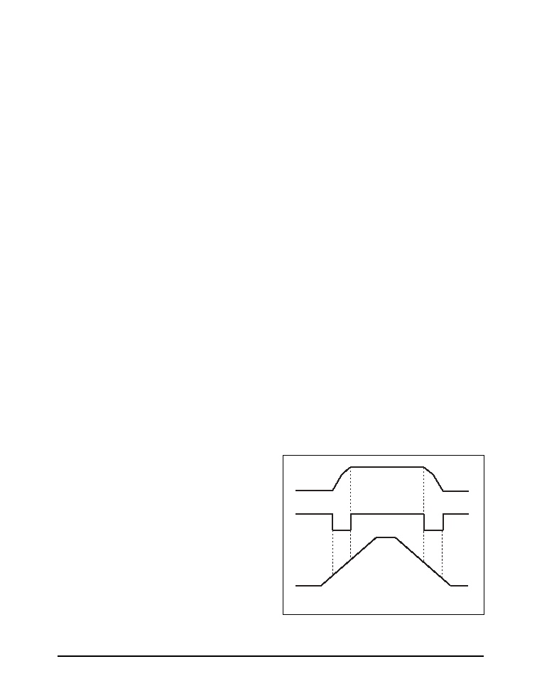
Error Detection Comparator Output
The Comparator produces a logic low output
whenever the SPX2945 output falls out of regu-
lation by more than around 5%. This is around
60mV offset divided by the 1.235 reference
voltage. This trip level remains 5% below
normal regardless of the programmed output
voltage of the regulator. Figure 1 shows the
timing diagram depicting the ERROR signal
and the regulator output voltage as the SPX2945
input is ramped up and down. The ERROR
signal becomes low at around 1.3V input, and
goes high around 5V input (input voltage at
which V
OUT
= 4.75). Since the SPX2945's
dropout voltage is load dependent, the input
voltage trip point (around 5V) will vary with the
load current. The output voltage trip point
(approx. 4.75V) does not vary with load.
The error comparator has an open-collector out-
put, which requires an external pull-up resistor.
Depending on the system requirements the re-
sistor may be returned to 5V output or other
supply voltage. In determining the value of this
resistor, note that the output is rated to sink
400
µA; this value adds to battery drain in a low
battery condition. Suggested values range from
100K to 1M
. If the output is unused this
resistor is not required.
Programming the Output Voltage of
SPX2945
The SPX2945 may be pin-strapped for 5V or
3.3V using its internal voltage divider by tying
Pin 1 (output) to Pin 2 (sense) and Pin 7 (feed-
back) to Pin 6 (5V/3.3V Tap).
Also, it may be programmed for any output
voltage between its 1.235V reference and its
20V maximum rating. As seen in Figure 2, an
external pair of resistors is required.
Refer to the below equation for the program-
ming of the output voltage::
V
OUT
= V
REF
x ( 1 + R
1
/ R
2
)+ I
FB
R
1
The V
REF
is 1.235 and I
FB
is the feedback bias
current, nominally -20nA. The minimum rec-
ommended load current of 1
µA forces an upper
limit of 1.2 M
on value of R
2
. If no load is
presented the I
FB
produces an error of typically
2% in V
OUT
, which may be eliminated at room
temperature by trimming R
1
. To improve the
accuracy choose the value of R
2
= 100k; this
reduces the error by 0.17% and increases the
resistor program current by 12
µA. Since the
SPX2945 typically draws 60
µA at no load with
Pin 2 open-circuited this is a small price to pay.
Reducing Output Noise
It may be an advantage to reduce the AC noise
present at the output. One way is to reduce the
regulator bandwidth by increasing the size of
the output capacitor. This is the only way that
noise can be reduced on the 3 lead SPX2945 but
is relatively inefficient, as increasing the ca-
pacitor from 1
µF to 220µF only decreases the
noise from 430
µV to 160µV Vrms for a 100kHz
bandwidth at 5V output. Noise could also be
reduced fourfold by a bypass capacitor across
R
1
, since it reduces the high frequency gain from
4 to unity. Pick
C
BYPASS
1 / 2R
1
x 200 Hz
or choose 0.01
µF. When doing this, the output
capacitor must be increased to 3.3
µF to main-
tain stability. These changes reduce the output
noise from 430
µV to 100µV Vrms for a 100kHz
bandwidth at 5V output. With the bypass ca-
pacitor added, noise no longer scales with out-
put voltage so that improvements are more dra-
matic at higher output voltages.
+
+
+
+
4.75V
OUTPUT
VOLTAGE
ERROR*
_______
INPUT
VOLTAGE
1.3V
5.0V
* See Application Info.
Figure 1. ERROR Output Timing
6
Rev. B Date:01/20/04
SPX2945 400mA Low Dropout Voltage Regulator with Shutdown
©Copyright 2004 Sipex Corporation
4
3
2
1
E
b
2
-A-
L
2
D
L
3
L
1
b
1
e
-C-
e1
D
1
E
1
BACK VIEW A-A
TERM 4
C
.010
M
A M
3 PLCS
-B-
A
A
1
C
1
c
8
A
A
SEATING
PLANE
H
L
NOTES
1. Refer To Applicable Symbol List.
2. Dimensions And Tolerancing Per Ansi Y14.5m - 1982.
3. Lead Dimension Uncontrolled in L3
4. Tab Contour Optional Within Dim. b2 & L2 And E1 & D1
5. D1 & E1 Establishes A Minimum Mounting Surface for
Terminal 4.
6. L is the Termal Length for Soldering.
7. Controlling Dimension: Inch
8. 2 Mils Suggested For Postive Contact At Mounting.
S
Y
M
B
O
L
MIN.
N
O
T
E
INCHES
MAX
MIN.
MAX
0.098
0.180
2.184
0.889
0.635
7.620
5.207
0.457
0.457
5.969
4.318
6.350
4.318
9.398
0.508
0.635
0.889
1.143
4
4,5
4,5
6
4
3
MM
2.3876
1.143
0.889
1.143
5.461
0.5842
0.5842
6.223
-
6.731
-
10.414
-
1.016
1.270
1.524
A
A1
b
b1
b2
c
c1
D
D1
E
E1
e
e1
H
L
L1
L2
L3
0.086
0.035
0.025
0.300
0.205
0.018
0.018
0.235
0.170
0.250
0.170
0.370
0.020
0.025
0.035
0.045
0.094
0.045
0.035
0.045
0.215
0.023
0.023
0.245
-
0.265
-
0.410
-
0.040
0.050
0.060
2.489
4.572
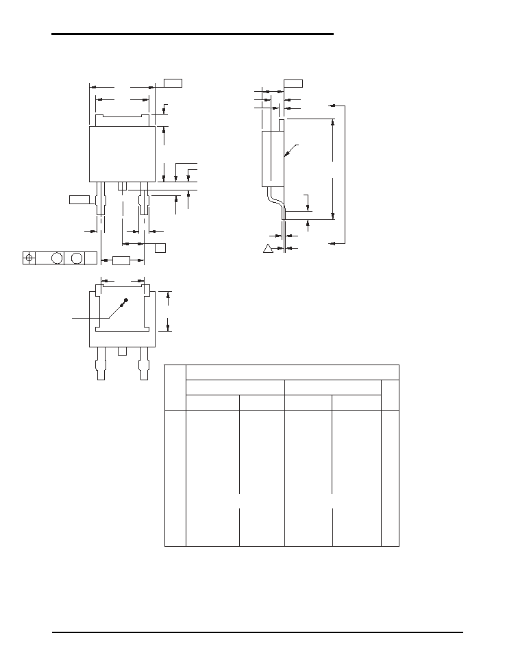
PACKAGE: 3 PIN TO-252
7
Rev. B Date:01/20/04
SPX2945 400mA Low Dropout Voltage Regulator with Shutdown
©Copyright 2004 Sipex Corporation
0.408
±
0.013
(10.36
±
0.33)
0.110
±
0.010
(2.794
±
0.254)
0.250
±
0.010
(6.350
±
0.254)
0.151D
±
0.002
(3.835 D
±
0.051)
0.180
±
0.005
(4.572
±
0.127)
0.050
±
0.002
(1.270
±
0.051)
0.340
±
0.010
(8.636
±
0.254)
0.150 MIN
(3.81 MIN)
0.410
(10.41)
0.100
±
0.010
(2.540
±
0.254)
0.032
±
0.005
(0.813
±
0.127)
0.540
±
0.015
(13.720
±
0.381)
0.050 TYP
(1.27 TYP)
0.200
±
0.010
(5.080
±
0.254)
0.015
±
0.010/-0.002
(0.381
±
0.254/-0.051)
0.015
±
0.010/-0.015
(2.667
±
0.254/-0.381)
1.020
±
0.015
(25.910
±
0.381)
SEATING
PLANE
Tapered 1
∞
2 Sides
7
∞
Typ.
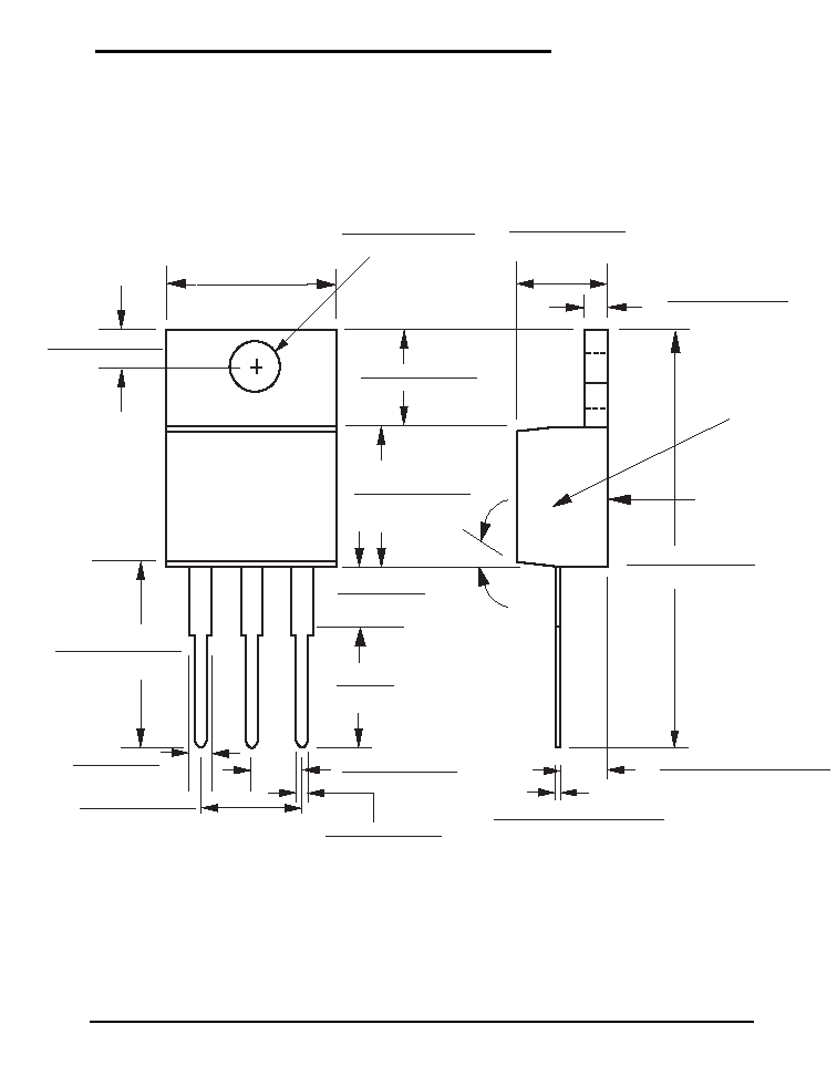
PACKAGE: 3 PIN TO-220
8
Rev. B Date:01/20/04
SPX2945 400mA Low Dropout Voltage Regulator with Shutdown
©Copyright 2004 Sipex Corporation
0.405 ± 0.005
(10.287 ± 0.127)
(9.042
0.127)
±
(15.24
0.635)
±
0.600
0.025
±
(0.813
0.076)
±
0.032
0.003
±
0.356 ± 0.005
0.055 (1.397)
0.176 ± 0.005 (4.470 ± 0.127)
0.050 ± 0.002 (1.270 ± 0.051)
0.015 +- 0.003
0∞ 8∞
(0.381
0.074)
+-
0.100
0.010
(2.540
0.254)
±
±
(1.702
0.127)
±
0.067
0.005
±
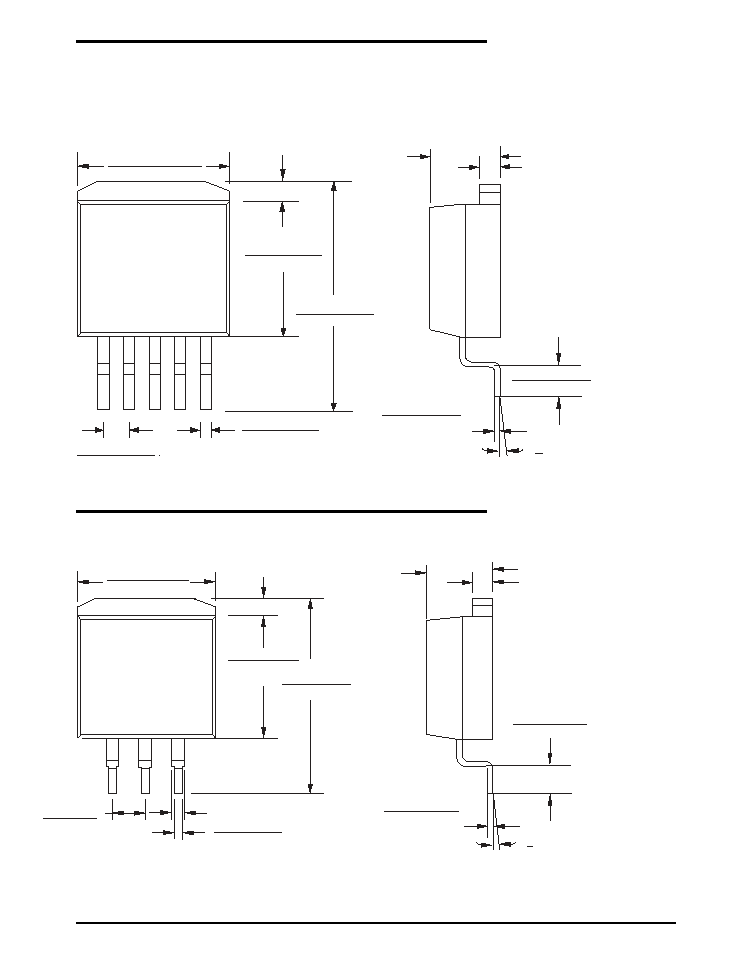
PACKAGE: 5 PIN TO-263
0.103 BSC
0.356
0.005
(9.042
0.127)
±
±
(15.24 0.635)
±
(2.616)
0.032
+-
0.001
(0.813
0.025)
+-
0.176 0.005
0.050 0.002
0.015
+-
0.003
0∞ 8∞
(0.381
0.074)
+
-
0.100
0.010
(2.540
0.254)
±
±
(4.470
0.127)
±
(1.270
0.051)
±
±
±
0.050 (1.270)
0.405 ± 0.005
(10.287 ± 0.127)
0.055 (1.397)
0.600 ± 0.025
PACKAGE: 3 PIN TO-263
9
Rev. B Date:01/20/04
SPX2945 400mA Low Dropout Voltage Regulator with Shutdown
©Copyright 2004 Sipex Corporation
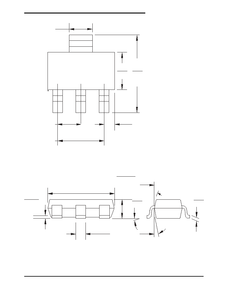
PACKAGE: 3 PIN SOT-223
0.116
0.124
0.146
0.130
0.295
0.264
0.041
0.033
0.0905 NOM
0.181 NOM
0.264
0.248
0.0040
0.0008
0.033
0.025
0.067
0.028
0.014
0.010
10
∞
C
16
∞
C
10
∞
C
16
∞
C
10
∞
C Max

10
Rev. B Date:01/20/04
SPX2945 400mA Low Dropout Voltage Regulator with Shutdown
©Copyright 2004 Sipex Corporation
ÿ
ÿ1
1.65
TOP VIEW
SEE VIEW C
8 PIN NSOIC
DIMENSIONS
Minimum/Maximum
(mm)
8 Pin NSOIC
(JEDEC MS-012,
AA - VARIATION)
COMMON HEIGHT DIMENSION
A
A1
A2
b
c
L
e
E1
E
L2
L1
1.35
4.90 BSC
0.40
0.31
0.51
SYMBOL
MIN NOM MAX
0.10
-
0.25
D
1.75
1.25
0.17
0.25
6.00 BSC
3.90 BSC
1.27 BSC
1.27
1.04 REF
0.25 BSC
0∫
5∫
8∫
15∫
L1
L
ÿ
ÿ1
ÿ1
Seating Plane
Gauge Plane
L2
VIEW C
A
A2
A1
SEATING PLANE
SIDE VIEW
e
E
E/2
E1
A
INDEX AREA
(D/2 X E1/2)
E1/2
D
b
1
c
WITH PLATING
BASE METAL
b
CONTACT AREA
-
-
-
-
-
-
-
PACKAGE: 8 PIN NSOIC
11
Rev. B Date:01/20/04
SPX2945 400mA Low Dropout Voltage Regulator with Shutdown
©Copyright 2004 Sipex Corporation
Corporation
ANALOG EXCELLENCE
Sipex Corporation reserves the right to make changes to any products described herein. Sipex does not assume any liability arising out of the
application or use of any product or circuit described herein; neither does it convey any license under its patent rights nor the rights of others.
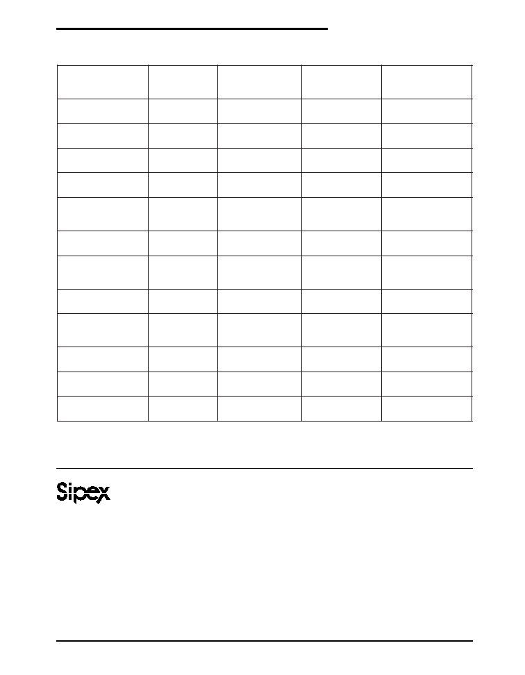
ORDERING INFORMATION
.
o
N
g
n
i
r
e
d
r
O
k
r
a
M
p
o
T
y
c
a
r
u
c
c
A
e
g
a
t
l
o
V
t
u
p
t
u
O
s
e
g
a
k
c
a
P
3
.
3
-
3
M
5
4
9
2
X
P
S
3
M
5
4
9
2
W
W
Y
Y
3
3
%
1
V
3
.
3
3
2
2
-
T
O
S
n
i
P
-
3
0
.
5
-
3
M
5
4
9
2
X
P
S
3
M
5
4
9
2
W
W
Y
Y
0
5
%
1
V
0
.
5
3
2
2
-
T
O
S
n
i
P
-
3
3
.
3
-
S
5
4
9
2
X
P
S
3
3
S
5
4
9
2
W
W
Y
Y
3
3
%
1
V
3
.
3
C
I
O
S
n
i
P
-
8
0
.
5
-
S
5
4
9
2
X
P
S
R
5
4
9
2
X
P
S
W
W
Y
Y
0
5
%
1
V
0
.
5
C
I
O
S
n
i
P
-
8
3
.
3
-
R
5
4
9
2
X
P
S
R
5
4
9
2
X
P
S
W
W
Y
Y
4
0
5
%
1
V
3
.
3
2
5
2
-
O
T
n
i
P
-
3
0
.
5
-
R
5
4
9
2
X
P
S
R
5
4
9
2
X
P
S
W
W
Y
Y
%
1
V
0
.
5
2
5
2
-
O
T
n
i
P
-
3
3
.
3
-
T
5
4
9
2
X
P
S
T
5
4
9
2
X
P
S
W
W
Y
Y
3
3
%
1
V
3
.
3
3
6
2
-
O
T
n
i
P
-
3
0
.
5
-
T
5
4
9
2
X
P
S
5
T
5
4
9
2
X
P
S
W
W
Y
Y
0
5
%
1
V
0
.
5
3
6
2
-
O
T
n
i
P
-
3
3
.
3
-
5
T
5
4
9
2
X
P
S
5
T
5
4
9
2
X
P
S
W
W
Y
Y
3
3
%
1
V
3
.
3
3
6
2
-
O
T
n
i
P
-
5
0
.
5
-
5
T
5
4
9
2
X
P
S
T
5
4
9
2
X
P
S
W
W
Y
Y
0
5
%
1
V
0
.
5
3
6
2
-
O
T
n
i
P
-
5
3
.
3
-
U
5
4
9
2
X
P
S
U
5
4
9
2
X
P
S
W
W
Y
Y
3
3
%
1
V
3
.
3
0
2
2
-
O
T
n
i
P
-
3
0
.
5
-
U
5
4
9
2
X
P
S
U
5
4
9
2
X
P
S
W
W
Y
Y
0
5
%
1
V
0
.
5
0
2
2
-
O
T
n
i
P
-
3
Sales Office
22 Linnell Circle
Billerica, MA 01821
TEL: (978) 667-8700
FAX: (978) 670-9001
e-mail: sales@sipex.com
Sipex Corporation
Headquarters and
Sales Office
233 South Hillview Drive
Milpitas, CA 95035
TEL: (408) 934-7500
FAX: (408) 935-7600