1
Rev:A Date: 3/8/04
SPX29500/01/02/03 5A Low Dropout Voltage Regulator
© Copyright 2004 Sipex Corporation
5A Low Dropout Voltage Regulator
Adjustable & Fixed Output, Fast Response Time
SPX29500/01/02/03
DESCRIPTION
FEATURES
Adjustable Output Down to 1.25V
1% Output Accuracy
Output Current of 5A
Low Dropout Voltage: 370mV @ 5A
Tight Line Regulation: 0.06%
Load Regulation: 0.2%
Fast Transient Response
Reverse-Battery Protection
Current Limit and Thermal Protection
Æ
The SPX29500/01/02/03 are 5A highly accurate voltage regulators with a low dropout voltage of 370mV
@ 5A. These regulators are specifically designed for low voltage applications that require a low dropout
voltage and a fast transient response. They are fully fault protected against over-current, reverse
battery, and positive and negative voltage transients. On-Chip trimming adjusts the reference voltage
to 1% initial accuracy. Other features in the 5 pin versions include Enable, and Error Flag.
The SPX29500/01/02/03 are offered in 3 & 5-pin TO-220 & TO-263 packages. For a 1.5A version, refer
to the SPX29150 data sheet. For a 3A version, refer to the SPX29300 datasheet.
APPLICATIONS
Powering VGA & Sound Card
Power PCTM Supplies
SMPS Post Regulator
High Efficiency "Green" Computer
Systems
High Efficiency Linear Power Supplies
Constant Current Regulators
Adjustable Power Supplies
Battery Charger
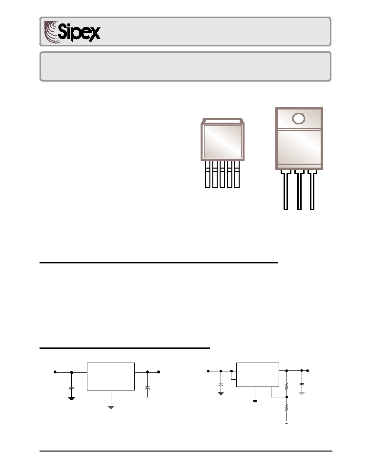
Figure 1. Fixed Output Linear Regulator
Figure 2. Adjustable Output Linear Regulator
SPX29502
V
OUT
V
IN
GND
ADJ
1
2
3
4
5
R1
R2
6.8µF
+
+
22µF
SPX29500
V
OUT
V
IN
6.8µF
+
+
22µF
1
2
3
TYPICAL APPLICATION CIRCUITS
1
2
3
SPX29502
5 Pin TO-263
EN
INPUT
GND
OUTPUT
ADJUST
GND V
OUT
V
IN
3
2
1
SP29500
3 Pin TO-220
Rev:A Date: 3/8/04
SPX29500/01/02/03 5A Low Dropout Voltage Regulator
© Copyright 2004 Sipex Corporation
2
ABSOLUTE MAXIMUM RATINGS
Lead Temperature (soldering, 5 seconds) ................260∞C
Storage Temperature Range........................-65∞C to +150∞C
Operating Junction Temperature Range......-40∞C to +125∞C
Input Voltage (Note 1) .................................................... 20V
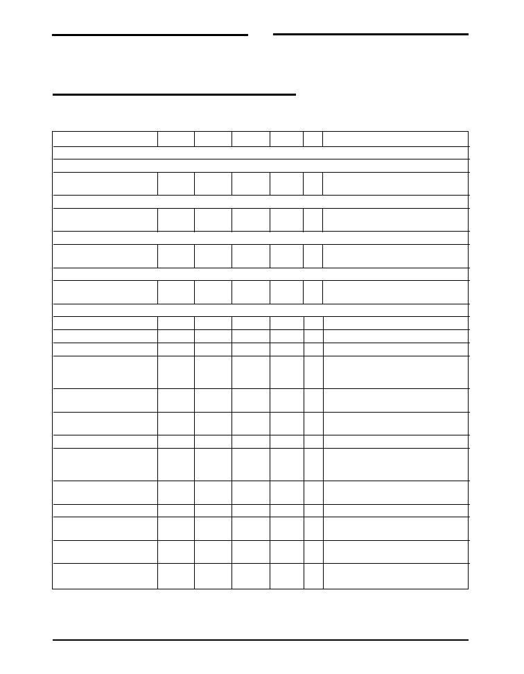
ELECTRICAL CHARACTERISTICS
Specifications are at V
IN
= V
OUT
+ 1V and I
OUT
= 10mA, C
IN
= 6.8
µF, C
OUT
= 22
µF, T
A
= 25
∞C, unless otherwise specified.
The
denotes the specifications which apply over the full operating temperature range, unless otherwise specified.
PARAMETER
MIN
TYP
MAX
UNITS
CONDITIONS
Fixed Voltage Options
SPX29500/01
1.8V Version
Output Voltage
1.782
1.800
1.818
V
I
OUT
= 10mA
1.764
1.800
1.836
10mA I
OUT
5A, 2.8V V
IN
16V
2.5V Version
Output Voltage
2.475
2.500
2.525
V
I
OUT
= 10mA
2.450
2.500
2.550
10mA I
OUT
5A, 3.5V V
IN
16V
3.3V Version
Output Voltage
3.267
3.300
3.333
V
I
OUT
= 10mA
3.234
3.300
3.366
10mA I
OUT
5A, 4.3V V
IN
16V
5.0V Version
Output Voltage
4.950
5.000
5.050
V
I
OUT
= 10mA
4.900
5.000
5.100
10mA I
OUT
5A, 6.0V V
IN
16V
All Voltage Options
SPX29500/01/02/03
Line Regulation
0.06
0.5
%
I
OUT
=10mA,(V
OUT
+1V) V
IN
16V
Load Regulation
0.2
1
%
V
IN
=V
OUT
+2V, 10mA I
OUT
I
FL
(Note 2)
V/T
20
100
ppm/∞C
V
OUT
Temp Coefficient (Note 5)
Dropout Voltage, except
80
250
mV
I
OUT
=250mA
1.8V
200
I
OUT
=2.5A
370
600
I
OUT
=5A
Ground Current
20
50
mA
I
OUT
=2.5A
(Note 4)
70
I
OUT
=5A
Ground Pin Current
3
mA
V
IN
=0.5V less than specified V
OUT,
at Dropout
I
OUT
=10mA
Current Limit
7.5
10
A
(Note 3)
Output Noise Voltage
425
µV
RMS
C
L
=22µF
(10Hz to 100kHz)
I
L
=100mA
350
C
L
=33µF
Reference Voltage
1.228
1.240
1.252
V
Adjustable version only
1.215
1.265
Reference Voltage
1.203
1.277
V
Adjustable version only (Note 7)
Adjust Pin Bias Current
40
80
nA
120
Reference Voltage
20
ppm/∞C
(Note 6)
Temp. Coeff.
Adjust Pin Bias
0.1
nA/∞C
Current Temp. Coeff.
OPERATING RATINGS
Input Voltage ................................................................... 16V
3
Rev:A Date: 3/8/04
SPX29500/01/02/03 5A Low Dropout Voltage Regulator
© Copyright 2004 Sipex Corporation
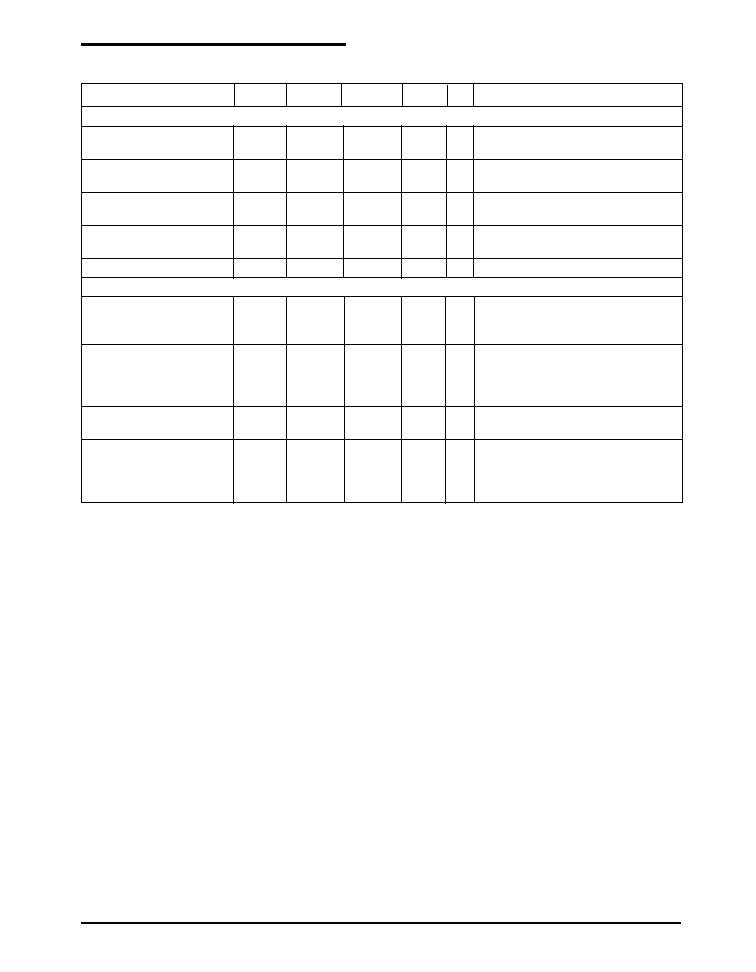
ELECTRICAL CHARACTERISTICS: Continued
Specifications are at V
IN
= V
OUT
+ 1V and I
OUT
= 10mA, C
IN
= 6.8
µF, C
OUT
= 22
µF, T
A
= 25
∞C, unless otherwise specified.
The
denotes the specifications which apply over the full operating temperature range, unless otherwise specified.
PARAMETER
MIN
TYP
MAX
UNITS
CONDITIONS
Flag Output
(Error Comparator)
SPX29501/03
Output Leakage
0.01
1
µA
V
OH
=16V
Current
2
Output Low Voltage
220
300
mV
Device set for 5V,V
IN
=4.5V, I
OL
=250µA
400
Upper Threshold
40
60
mV
Device set for 5V, (Note 8)
Voltage
25
Lower Threshold
75
95
mV
Device set for 5V, (Note 8)
Voltage
140
Hysteresis
15
mV
Device set for 5V, (Note 8)
Enable Input
SPX29501/02
Input Logic Voltage
Low (OFF)
0.8
V
(Note 10)
High (ON)
2.4
ENABLE Input Current
100
600
µA
V
EN
=16V
750
0.6
2
µA
V
EN
=0.8V
4
Regulator Output
10
µA
(Note 9)
Current in Shutdown
500
Thermal Resistance
2
∞C/W
TO-220 Junction to Case, at Tab
60
TO-220 Junction to Ambient
2
TO-263 Junction to Case, at Tab
60
TO-263 Junction to Ambient
NOTES:
Note 1: Maximum positive supply voltage of 20V must be of limited duration (<100ms) and duty cycle of less than 1%. The
maximum continuous supply voltage is 16V.
Note 2: Full load current (I
FL
) is defined as 5A.
Note 3: V
IN
= V
OUT
(NOMINAL)
+1V. For example, use V
IN
= 4.3V for a 3.3V regulator. Employ pulse-testing procedures to minimize
temperature rise.
Note 4 Ground pin current is the regulator quiescent current. The total current drawn from the source is the sum of the load current
plus the ground pin current.
Note 5: Output voltage temperature coefficient is defined as the worst case voltage change divided by the total temperature range.
Note 6: Thermal regulation is defined as the change in output voltage at time T after a change in power dissipation is applied,
excluding load / line regulation effects. Specifications for a 200mA load pulse as V
IN
= 20V (a 4W pulse) for t = 10ms.
Note 7: V
REF
V
OUT
(V
IN
-1), 2.3VV
IN
16V, 10mA I
L
I
FL
, T
j
< T
jmax
.
Note 8: Comparator threshold is expressed in terms of a voltage differential at the Adjust terminal below the nominal reference
voltage measured 6V input. To express these thresholds in terms of output voltage change, multiply the error amplifier gain =
V
OUT
/V
REF
= (R1 + R2)/R2. For example, at a programmable output voltage of 5V, the Error output is guaranteed to go low when
the output drops by 95mVx 5V/ 1.240V = 383mV. Threshold remain constant as a percent of V
OUT
as V
OUT
is varied, with the
dropout warning occurring at typically 5% below nominal, 7.7% guaranteed.
Note 9: V
EN
0.4V and V
IN
16V, V
OUT
= 0.
Note 10: Measured with I
OUT
= I
OUT
MIN (10mA).
Rev:A Date: 3/8/04
SPX29500/01/02/03 5A Low Dropout Voltage Regulator
© Copyright 2004 Sipex Corporation
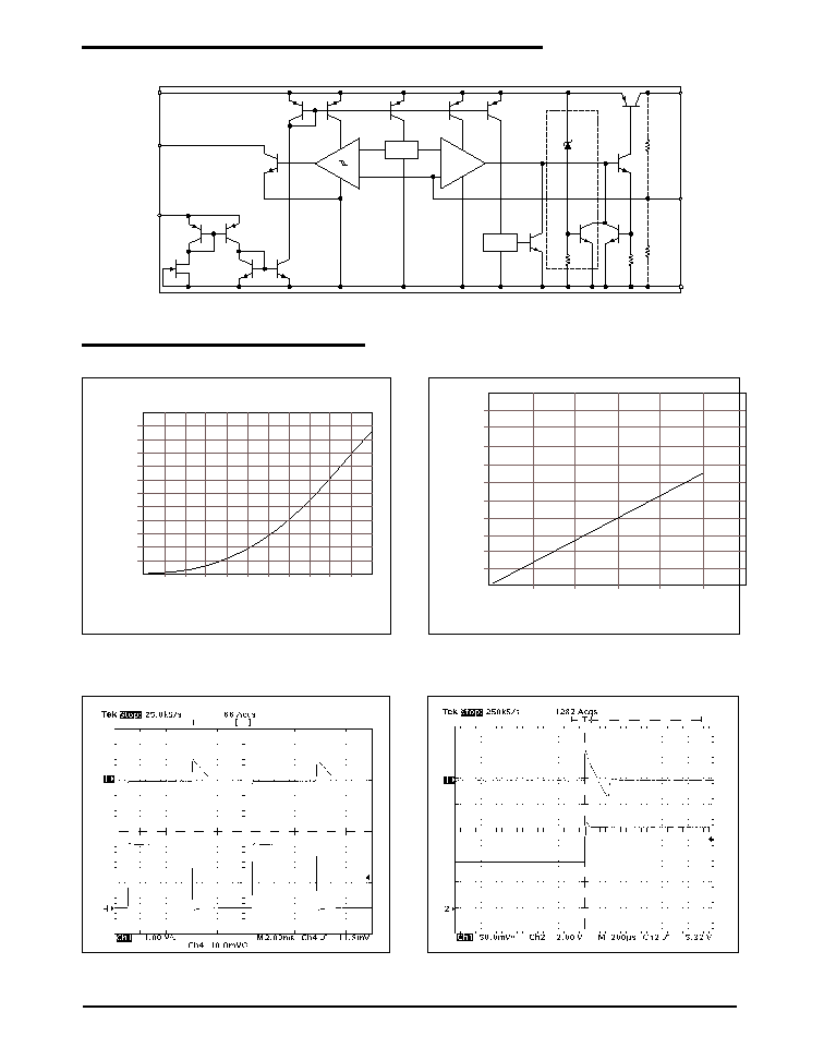
4
V
OUT
(AC)
I
OUT
(2A/DIV)
V
OUT
(AC)
V
IN
Reference
Thermal
Shutdown
EN
IN
OUT
ADJ
GND
O.V
I
LIMIT
20V
R1*
R2*
1.180V
1.240V
+
+
-
-
FLAG
FUNCTIONAL DIAGRAM
TYPICAL PERFORMANCE CHARACTERISTICS
0
10
20
30
40
50
60
70
80
90
100
110
120
Ground Current (mA)
0
1
2
3
4
5
Output Current (A)
Figure 3. Ground Current (mA) vs. Output Current (A)
Figure 4. Dropout (mV) vs. Output Current (A)
600
550
500
450
400
350
300
250
200
150
100
50
0
1
2
3
4
5
6
Output Current (A)
Dropout (mA)
Figure 5. Load Transient (V
IN
=4V, V
O
=3.3V, C
OUT
=22
µF,
10mA~5A)
Figure 6. Line Transient (C
OUT
=22
µF, I
O
=10mA)

5
Rev:A Date: 3/8/04
SPX29500/01/02/03 5A Low Dropout Voltage Regulator
© Copyright 2004 Sipex Corporation
APPLICATION INFORMATION
The SPX29500/01/02/03 incorporates protec-
tion against over-current faults, reversed load
insertion, over temperature operation, and posi-
tive and negative transient voltage.
Thermal Considerations
Although the SPX29500/01/02/03 offers limit-
ing circuitry for overload conditions, it is still
necessary to insure that the maximum junction
temperature is not exceeded in the application.
Heat will flow through the lowest resistance
path, the junction-to-case path. In order to insure
the best thermal flow of the component, proper
mounting is required.
TO-220 Design Example:
Assume that V
IN
= 8V, V
OUT
= 5V, I
OUT
= 5A, T
A
= 50
∞C,
HA
= 1
∞C/W,
CH
= 2
∞C/W, and
JC
=
2
∞C/W, where:
T
A
= ambient temperature,
HA
= heatsink to ambient thermal
resistance
CH
= case to heatsink thermal
resistance
JC
= junction to case thermal
resistance
The power calculated under these conditions is:
P
D
= (V
IN
≠ V
OUT
) * I
OUT
= 15W.
And the junction temperature is calculated as
T
J
= T
A
+ P
D
* (
HA
+
CH
+
JC
) or
T
J
= 50 + 15 * (1+2+2) = 125
∞C
Reliable operation is insured.
Capacitor Requirements
The output capacitor is needed to insure stability
and minimize the output noise. The value of the
capacitor varies with the load. However, a
minimum value of 22
µF aluminum capacitor
will guarantee stability over all load conditions.
A tantalum capacitor is recommended if a faster
load transient response is needed. If the power
source has a high AC impedance, a 0.1
µF ce-
ramic capacitor between input & ground is rec-
ommended.
Minimum Load Current
To ensure a proper behavior of the regulator
under light load, a minimum load of 10mA for
SPX29500/01/02/03 is required.
Adjustable Regulator Design
The SPX29502/03 are adjustable regulators that
can be programmed to any value between 1.24V
and 16V using 2 resistors, R1 and R2. The
relationship between the resistors is:
R1 = R2(V
OUT
/1.24-1).
Error Flag
The SPX29501/03 features an error flag that
indicates either an over current or under voltage
condition. The flag output goes low, sinking
10mA when either condition occurs.
Enable Input
The SPX29501/02 have an Enable function that
switches the regulator on and off. Their thresh-
olds are TTL compatible. Enabling the regulator
requires approximately 20
µA of current.
Typical Application Circuits
Figure 1 represents at typical fixed output regu-
lator. Figure 2 represents an adjustable output
regulator. The values of R1 and R2 set the output
voltage value as follows:
V
OUT
=V
REF
* [1 + (R1/R2)].
For best results, the total series resistance should
guarantee a minimum regulator load current of
10mA.