 | –≠–ª–µ–∫—Ç—Ä–æ–Ω–Ω—ã–π –∫–æ–º–ø–æ–Ω–µ–Ω—Ç: SPX2969W1 | –°–∫–∞—á–∞—Ç—å:  PDF PDF  ZIP ZIP |

1
Date: 8/4/04 SPX2969 150mA Low Dropout Voltage Regulator
© Copyright 2004 Sipex Corporation
150mA Low Dropout Voltage Regulator
SPX2969
DESCRIPTION
FEATURES
5V Fixed Output
150mA current capability
250mV Dropout
Programmable Reset Threshold
250µA Quiescent Current
Over Temperature Protection
Reverse Polarity Protection
Integrated Pull Up Resistor on Logic Outputs
-40∞ to 125∞C Operating Range
Available in 8 Pin and 14 Pin nSOIC or 20
Pin wSOIC packages.
Æ
Sipex's SPX2969 is a low dropout linear regulator with integrated PNP pass transistor. The part
is designed for automotive environment, and thus can withstand up to 45V and 125∞C
temperature range. The output voltage is set at a fixed 5V, and the part is guaranteed to deliver
at least 150mA. The SPX2969 provides multiple protection mechanisms, including over-
temperature and over-current conditions. The part has a built-in reset circuit to monitor when the
output voltage is below 4.65V. The reset voltage threshold can be programmed down to 3.5V
using an external resistor voltage divider, while the reset timing can be programmed via an
external capacitor. A built in comparator compares the signal of the pin SI, normally fed by a
voltage divider from the input voltage, with the reference and gives an early warning on the pin
SO. Both the sense output and the reset output delay signals contain integrated 20kOhm pull up
resistors. The part is available in three package types: 8 Pin and 14 Pin nSOIC or 20 Pin wSOIC
packages.
TYPICAL APPLICATION CIRCUIT
Advanced
GND
I
Q
SO
D
SI
12V
RO
5V
SPX2969
RADJ2
RADJ1 +
+
22µF
1000µF
RS1
RS2
0.1µF
RESET OUT
RADJ
APPLICATIONS
Automotive
Industrial
Wireless Base Station
1
2
3
4
5
6
7
8
I
SPX2969
8 PIN NSOIC
GND
SI
SO
RO
D
Q
RADJ
Now Available in Lead Free Packaging
2
Date: 8/4/04 SPX2969 150mA Low Dropout Voltage Regulator
© Copyright 2004 Sipex Corporation
Input Voltage ...................................................................... -40V to 45V
Input Current ............................................................... internally limited
Sense Input Voltage ........................................................... -40V to 45V
Sense Input Current ......................................................... -1mA to 1mA
Reset Threshold Voltage ....................................................... -0.3 to 7V
Reset Threshold Current ................................................... -10 to 10mA
Reset Delay Voltage ............................................................. -0.3 to 7V
Reset Delay Current .................................................... internally limited
Ground Current .................................................................. 50mA (min)
Reset Output Voltage ............................................................ -0.3 to 7V
Reset Output Current .................................................. internally limited
Sense Output Voltage ........................................................... -0.3 to 7V
Sense Output Current ................................................. internally limited
Output Voltage ...................................................................... -0.3 to 7V
Output Current ............................................................ internally limited
Thermal Data
Junction Ambient (8 Pin NSOIC) ............................................. 163∞C/W
Junction Ambient (20 Pin WSOIC) ............................................ 70∞C/W
Junction Ambient (14 Pin NSOIC) ............................................. 70∞C/W
Storage Temperature .................................................. -50∞C to +150∞C
Junction Temperature.(Note 1)...........................................-50∞C+150∞C
These are stress ratings only and functional operation of the device at
these ratings or any other above those indicated in the operation sections
of the specifications below is not implied. Exposure to absolute maximum
rating conditions for extended periods of time may affect reliability.
ELECTRICAL CHARACTERISTICS
V
IN
= 13.5V; -40∞C < T
J
< 125∞C.
The
denotes the specifications which apply over the full operating temperature range, unless
otherwise specified.
ABSOLUTE MAXIMUM RATINGS
Note 1: Specifications in the -40∞C to 150∞C range are guaranteed by design, not production tested.
Note 2: Drop voltage = V
I
- V
Q
measured when the output voltage has dropped 100mV from the nominal value obtained at 13.5V input.
Note 3: The reset threshold V
RT
can be decreased via an external voltage divider connected to the RADJ. In this case the reset condition is reached if
V
Q
< V
RT
and V
RADJ
< V
RAQDJ, TH
. Dimensioning the voltage divider according to: V
THRES
= V
RADJ, TH
X (R
ADJ1
+R
ADJ2
)/R
ADJ2.
R
E
T
E
M
A
R
A
P
L
O
B
M
Y
S
N
I
M
P
Y
T
X
A
M
S
T
I
N
U
S
N
O
I
T
I
D
N
O
C
e
g
a
t
a
l
o
V
t
u
p
t
u
O
V
Q
0
9
.
4
0
0
.
5
0
1
.
5
V
I
<
A
m
1
Q
A
m
0
0
1
V
<
V
6
I
V
6
1
<
t
i
m
i
L
t
n
e
r
r
u
C
I
Q
0
5
1
0
5
2
0
0
5
A
m
-
t
n
e
r
r
u
C
n
o
i
t
p
m
u
s
n
o
C
I
q
I
=
I
I
-
Q
I
q
-
0
4
2
0
0
3
A
µ
I
Q
j
T
,
A
m
1
<
C
∞
5
8
<
t
n
e
r
r
u
C
n
o
i
t
p
m
u
s
n
o
C
I
q
I
=
I
I
-
Q
I
q
-
0
5
2
0
0
7
A
µ
I
Q
A
m
0
1
=
t
n
e
r
r
u
C
n
o
i
t
p
m
u
s
n
o
C
I
q
I
=
I
I
-
Q
I
q
-
2
8
A
m
I
Q
A
m
0
5
=
e
g
a
t
l
o
V
p
o
r
D
V
R
D
-
5
2
.
0
5
.
0
V
I
Q
s
p
o
r
d
t
u
p
t
u
o
n
e
h
w
)
I
-
Q
(
A
m
0
0
1
=
)
2
e
t
o
n
e
e
s
(
%
2
w
o
l
e
b
n
o
i
t
a
l
u
g
e
R
d
a
o
L
V
Q
-
2
0
2
V
m
I
Q
A
m
0
0
1
o
t
A
m
5
=
n
o
i
t
a
l
u
g
e
R
e
n
i
L
V
Q
-
1
0
1
V
m
V
I
V
6
2
o
t
V
6
=
I
Q
A
m
1
=
r
o
t
a
r
e
n
e
G
t
e
s
e
R
e
g
a
t
l
o
V
d
l
o
h
s
e
r
h
T
V
T
R
0
5
.
4
5
6
.
4
0
8
.
4
V
-
t
s
u
j
d
A
t
e
s
e
R
V
H
T
,
J
D
A
R
6
2
.
1
5
3
.
1
4
4
.
1
V
V
Q
)
3
e
t
o
n
e
e
s
(
V
5
.
3
=
p
u
ll
u
P
t
e
s
e
R
-
0
1
0
2
0
4
K
-
e
g
a
t
l
o
V
n
o
i
t
a
r
u
t
a
S
V
T
A
S
,
O
R
-
1
.
0
4
.
0
V
R
n
r
e
t
n
i
3
Date: 8/4/04 SPX2969 150mA Low Dropout Voltage Regulator
© Copyright 2004 Sipex Corporation
ELECTRICAL CHARACTERISTICS
V
IN
= 13.5V; -40∞C < T
J
< 125∞C.
The
denotes the specifications which apply over the full operating temperature range, unless
otherwise specified.
R
E
T
E
M
A
R
A
P
L
O
B
M
Y
S
N
I
M
P
Y
T
X
A
M
S
T
I
N
U
S
N
O
I
T
I
D
N
O
C
r
o
t
a
r
e
n
e
G
t
e
s
e
R
g
n
i
h
c
t
i
w
S
y
a
l
e
D
r
e
p
p
U
d
l
o
h
s
e
r
h
T
V
D
U
4
.
1
8
.
1
2
.
2
V
-
g
n
i
h
c
t
i
w
S
y
a
l
e
D
r
e
w
o
L
d
l
o
h
s
e
r
h
T
V
D
L
3
.
0
5
4
.
0
0
6
.
0
V
-
y
a
l
e
D
e
g
a
t
l
o
V
n
o
i
t
a
r
u
t
a
S
r
o
t
i
c
a
p
a
C
V
T
A
S
,
D
-
-
1
.
0
V
V
Q
V
<
T
R
t
n
e
r
r
u
C
e
g
r
a
h
C
I
D
0
.
3
5
.
6
5
.
9
A
µ
V
D
V
1
=
H
`
L
e
m
i
T
y
a
l
e
D
t
D
7
1
8
2
-
s
m
C
D
F
n
0
0
1
=
L
`
H
e
m
i
T
y
a
l
e
D
t
t
-
1
-
s
µ
C
D
F
n
0
0
1
=
e
s
n
e
S
e
g
a
t
l
o
V
t
u
p
n
I
h
g
i
H
d
l
o
h
s
e
r
h
T
e
s
n
e
S
V
h
g
i
h
,
I
S
4
2
.
1
1
3
.
1
8
3
.
1
V
-
w
o
L
d
l
o
h
s
e
r
h
T
e
s
n
e
S
V
w
o
l
,
I
S
6
1
.
1
0
2
.
1
8
2
.
1
V
-
e
g
a
t
l
o
V
w
o
l
t
u
p
t
u
O
e
s
n
e
S
V
w
o
l
,
O
S
-
1
.
0
4
.
0
V
V
I
S
V
0
2
.
1
<
V
Q
V
3
>
R
n
r
e
t
n
i
p
u
ll
u
P
e
s
n
e
S
-
0
1
0
2
0
4
K
-
t
n
e
r
r
u
C
t
u
p
n
I
e
s
n
e
S
i
i
s
1
-
1
.
0
1
A
µ
-
e
m
i
T
e
s
n
o
p
s
e
R
e
s
n
e
S
-
2
s
µ
-
4
Date: 8/4/04 SPX2969 150mA Low Dropout Voltage Regulator
© Copyright 2004 Sipex Corporation
APPLICATIONS INFORMATION
The input capacitor C
I
is necessary for compensating line influences. Using a resistor of
approximately 1 in series with C
I
, the oscillating circuit consisting of input inductivity and input
capacitance can be damped. The output capacitor C
Q
is necessary for the stability of the
regulating circuit. Stability is guarantted at values 10µF and an ESR 10 within the operating
temerature range. For small tolerances of the reset delay the spread of the capacitance of the
delay capacitor and its temperature coefficient should be noted.
REFERENCE
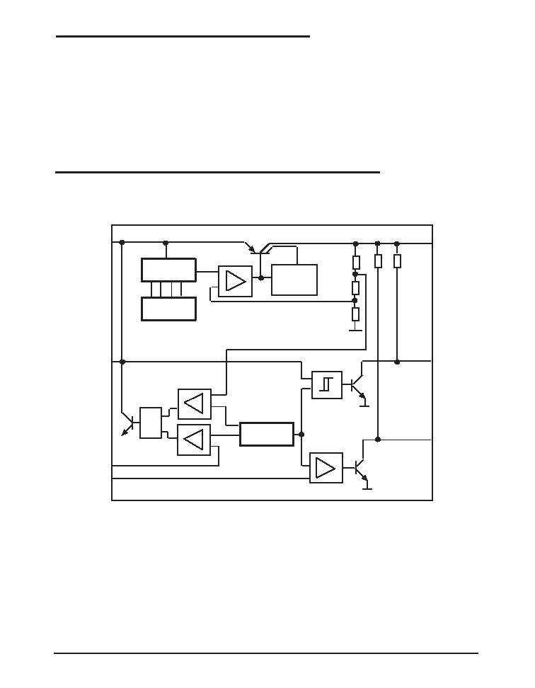
REFERENCE
TRIMMING
ERROR AMPLIFIER
SATURATION
CURRENT AND
CONTROL
&
SO
RO
Q
I
D
RADJ
SI
BLOCK DIAGRAM
5
Date: 8/4/04 SPX2969 150mA Low Dropout Voltage Regulator
© Copyright 2004 Sipex Corporation
PIN DESCRIPTION
R
E
B
M
U
N
N
I
P
E
M
A
N
N
I
P
)
C
I
O
N
N
I
P
8
(
N
O
I
T
P
I
R
C
S
E
D
1
V
N
I
.
r
o
t
i
c
a
p
a
c
c
i
m
a
r
e
C
a
h
t
i
w
D
N
G
o
t
k
c
o
l
b
.
t
u
p
n
I
2
N
I
E
S
N
E
S
Q
o
t
t
c
e
n
n
o
c
d
e
e
n
t
o
n
f
I
.
t
u
p
n
I
e
s
n
e
S
3
R
J
D
A
D
N
G
o
t
t
c
e
n
n
o
c
d
e
d
e
e
n
t
o
n
f
I
.
j
d
A
d
l
o
h
h
s
e
r
h
T
t
e
s
e
R
4
Y
A
L
E
D
.
r
o
t
i
c
a
p
a
c
a
i
v
D
N
G
o
t
t
c
e
n
n
o
c
,
e
m
i
t
y
a
l
e
d
t
c
e
l
e
s
o
T
.
y
a
l
e
D
t
e
s
e
R
5
D
N
G
d
n
u
o
r
G
6
T
E
S
E
R
t
i
p
e
e
K
.
r
o
t
s
i
s
e
r
a
a
i
v
Q
o
t
d
e
k
n
il
y
ll
a
n
r
e
t
n
i
s
i
t
u
p
t
u
o
r
o
t
c
e
ll
o
c
-
n
e
p
o
e
h
T
.
t
u
p
t
u
O
t
e
s
e
R
.
d
e
d
e
e
n
t
o
n
f
i
n
e
p
o
7
T
U
O
E
S
N
E
S
t
i
p
e
e
K
.
r
o
t
s
i
s
e
r
a
a
i
v
Q
o
t
d
e
k
n
il
y
ll
a
n
r
e
t
n
i
s
i
t
u
p
t
u
o
r
o
t
c
e
ll
o
c
-
n
e
p
o
e
h
T
.
t
u
p
t
u
O
e
s
n
e
S
.
d
e
d
e
e
n
t
o
n
f
i
n
e
p
o
8
V
T
U
O
0
1
<
R
S
E
,
r
o
t
i
c
a
p
a
c
F
µ
0
1
a
h
t
i
w
D
N
G
o
t
t
c
e
n
n
o
C
.
t
u
p
t
u
O
V
5
R
E
B
M
U
N
N
I
P
E
M
A
N
N
I
P
)
C
I
O
N
E
D
I
W
N
I
P
0
2
(
N
O
I
T
P
I
R
C
S
E
D
1
R
J
D
A
D
N
G
o
t
t
c
e
n
n
o
c
d
e
d
e
e
n
t
o
n
f
I
.j
d
A
d
l
o
h
s
e
r
h
T
t
e
s
e
R
2
Y
A
L
E
D
.
r
o
ti
c
a
p
a
c
a
i
v
D
N
G
o
t
t
c
e
n
n
o
c
,
e
m
it
y
a
l
e
d
t
c
e
l
e
s
o
T
.
y
a
l
e
d
t
e
s
e
R
3
C
N
t
c
e
n
n
o
C
o
N
4
D
N
G
d
n
u
o
r
G
5
D
N
G
d
n
u
o
r
G
6
D
N
G
d
n
u
o
r
G
7
D
N
G
d
n
u
o
r
G
8
C
N
t
c
e
n
n
o
c
o
N
9
C
N
t
c
e
n
n
o
c
o
N
0
1
T
E
S
E
R
p
e
e
K
.
r
o
t
s
i
s
e
r
p
u
ll
u
p
m
h
o
K
0
2
a
a
i
v
Q
o
t
d
e
k
n
il
y
ll
a
n
r
e
t
n
i
s
i
t
u
p
t
u
o
r
o
t
c
e
ll
o
c
-
n
e
p
o
e
h
T
.
t
u
p
t
u
O
t
e
s
e
R
.
d
e
d
e
e
n
t
o
n
fi
n
e
p
o
1
1
T
U
O
E
S
N
E
S
p
u
ll
u
p
m
h
o
k
0
2
a
a
i
v
t
u
p
t
u
o
e
h
t
o
t
d
e
k
n
il
y
ll
a
n
r
e
t
n
i
s
i
t
u
p
t
u
o
r
o
t
c
e
ll
o
c
n
e
p
o
e
h
T
.
t
u
p
t
u
o
e
s
n
e
S
.
d
e
d
e
e
n
t
o
n
fi
n
e
p
o
p
e
e
K
.
r
o
t
s
i
s
e
r
2
1
V
T
U
O
0
1
<
R
S
E
,
r
o
ti
c
a
p
a
c
F
u
0
1
a
h
ti
w
D
N
G
o
t
t
e
c
n
n
o
C
.
t
u
p
t
u
O
V
5
3
1
C
N
t
c
e
n
n
o
C
o
N
4
1
D
N
G
d
n
u
o
r
G
5
1
D
N
G
d
n
u
o
r
G
6
1
D
N
G
d
n
u
o
r
G
7
1
D
N
G
d
n
u
o
r
G
8
1
C
N
t
c
e
n
n
o
C
o
N
9
1
V
N
I
.
r
o
ti
c
a
p
a
c
c
i
m
a
r
e
c
a
h
ti
w
C
I
e
h
t
t
a
y
lt
c
e
r
i
d
D
N
G
o
t
s
s
a
p
y
B
.
t
u
p
n
I
0
2
N
I
E
S
N
E
S
V
o
t
t
c
e
n
n
o
c
d
e
d
e
e
n
t
o
n
f
I
.
t
u
p
n
I
e
s
n
e
S
T
U
O