
1
Rev. 2/3/03 SPX3940 1A Low Dropout Voltage Regulator
© Copyright 2003 Sipex Corporation
1A Low Dropout Voltage Regulator
Fixed Output, Fast Response
SPX3940
DESCRIPTION
FEATURES
1% Output Accuracy SPX3940A
Guaranteed 1.5A Peak Current
Low Quiescent Current
Low Dropout Voltage of 280mV at 1A
Extremely Tight Load and Line Regulation
Extremely Fast Transient Response
Reverse-battery Protection
Internal Thermal Protection
Internal Short Circuit Current Limit
Replacement for LM3940
Standard SOT-223, TO-220
and TO-263 packages
Æ
The SPX3940 is a 1A, accurate voltage regulators with a low drop out voltage of 280mV(typical)
at 1A. These regulators are specifically designed for low voltage applications that require a low
dropout voltage and a fast transient response. They are fully fault protected against over-current,
reverse battery, and positive and negative voltage transients.
The SPX3940 is offered in 3-pin SOT-223, TO-220 & TO-263 packages. For a 3A version, refer
to the SPX29300 data sheet.
APPLICATIONS
Powering VGA & Sound Card
Automotive Electronics
LCD Monitors
Cordless Telephones
Power PC
TM
Supplies
SMPS Post-Regulator
Laptop, Palmtop, and Notebook Computer
High Efficiency Linear Power Supplies
Portable Instrumentation
Constant Current Regulators
SPX3940
V
OUT
V
IN
+
6.8
µ
F
+
10
µ
F
1
2
3
Figure 1. Fixed Output Linear Regulator.
2
Rev. 2/3/03 SPX3940 1A Low Dropout Voltage Regulator
© Copyright 2003 Sipex Corporation
ABSOLUTE MAXIMUM RATINGS
Lead Temperature (soldering, 5 seconds) ................................. 260
∞
C
Storage Temperature Range ..................................... -65
∞
C to +150
∞
C
Operating Junction Temperature Range ................... -40
∞
C to +125
∞
C
Input Voltage (Note 5) ................................................................... 16V
NOTES:
Note 1: Dropout voltage is defined as the input to output differential when the output voltage drops to 99% of its normal value.
Note 2: V
IN
=V
OUT (NOMINAL)
+ 1V. For example, use V
IN
=4.3V for a 3.3V regulator. Employ pulse-testing procedures to minimize temperature rise.
Note 3: Ground pin current is the regulator quiescent current. The total current drawn from the source is the sum of the load current to the ground current.
Note 4: Thermal regulation is defined as the change in the output voltage at a time T after a change in power dissipation is applied, excluding load or line regulation effects.
Note 5: Maximum positive supply voltage of 20V must be of limited duration (<100ms) and duty cycle (<1%). The maximum continuous supply voltage is 16V.
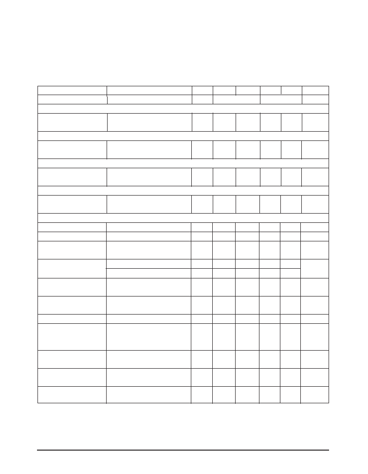
ELECTRICAL CHARACTERISTICS
At V
IN
=V
OUT
+ 1V and I
OUT
= 10 mA, C
IN
= 6.8
µ
F, C
OUT
= 10
µ
F; T
A
= 25
∞
C, unless otherwise specified.
The Boldface applies over the junction temperature range. Adjustable versions are set at 5.0V.
PARAMETER
CONDITIONS
TYP
MIN
MAX
MIN
MAX
UNITS
SPX3940A (1%)
SP3940 (2%)
1.8V Version
Output Voltage
I
OUT
= 10mA
1.8
1.782
1.818
1.764
1.836
V
10mA
I
OUT
1A, 6V
V
IN
16V
1.8
1.755
1.845
1.737
1.863
2.5V Version
Output Voltage
I
OUT
= 10mA
2.5
2.475
2.525
2.450
2.550
V
10mA
I
OUT
1A, 6V
V
IN
16V
2.5
2.437
2.563
2.412
2.588
3.3V Version
Output Voltage
I
OUT
= 10mA
3.3
3.267
3.333
3.234
3.366
V
10mA
I
OUT
1A, 6V
V
IN
16V
3.3
3.217
3.383
3.184
3.416
5.0V Version
Output Voltage
I
OUT
= 10mA
5.0
4.950
5.050
4.900
5.100
V
10mA
I
OUT
1A, 6V
V
IN
16V
5.0
4.875
5.125
4.825
5.175
All Voltage Options
Line Regulation
I
O
=10mA, (V
OUT
+1V)
V
IN
16V
0.2
1.0
1.0
%
Load Regulation
V
IN
=V
OUT
+1V, 10mA
I
OUT
1A
0.3
1.5
1.5
%
V
Output Voltage
20
100
100
ppm/
∞
C
T
Temperature Coef.
Dropout Voltage (Note 1)
I
O
=100mA
70
200
200
mV
(except 1.8V version)
I
O
=1A
280
550
550
Ground Current (Note 3)
I
O
=750mA, V
IN
=V
OUT
, + 1V
12
25
25
mA
I
O
=1A
18
I
GNDDO
Ground Pin
V
IN
=0.1V less than specified V
OUT
1.2
mA
Current at Dropout
I
OUT
= 10mA
Current Limit
V
OUT
=0V (Note 2)
2.2
1.5
1.5
A
Output Noise Voltage
C
L
= 10
µ
F
400
µ
V
RMS
(10Hz to 100kHz)
I
L
=100mA
C
L
=33
µ
F
260
Thermal Resistance
TO-220 Junction to Case, at Tab
3
∞
C/W
TO-220 Junction to Ambient
60
TO-263 Junction to Case, at Tab
3
∞
C/W
TO-263 Junction to Ambient
60
SOT-223 Junction to Case, at Tab
15
∞
C/W
SOT-223 Junction to Ambient
150
3
Rev. 2/3/03 SPX3940 1A Low Dropout Voltage Regulator
© Copyright 2003 Sipex Corporation
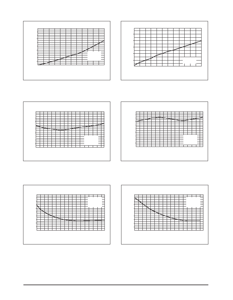
TYPICAL PERFORMANCE CHARACTERISTICS
Figure 2. Line Regulation
Figure 3. Load Regulation
Figure 4. Ground Current vs Load Current
Figure 5. Ground Current vs Input Voltage
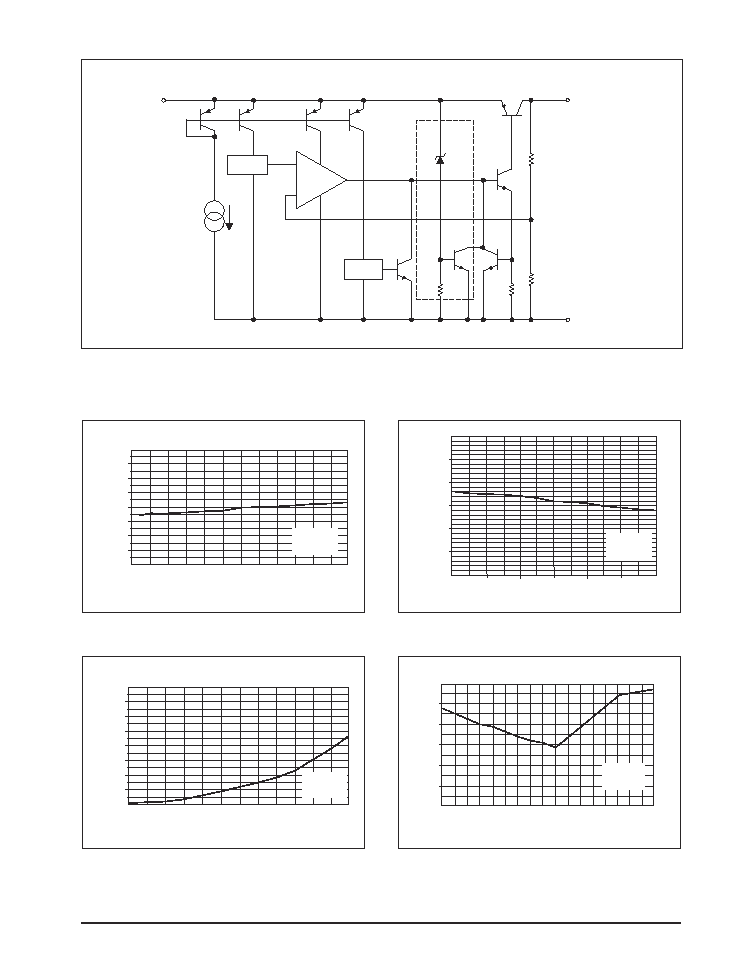
Reference
Thermal
Shutdown
IN
OUT
GND
O.V
I
LIMIT
28V
R1
R2
1.240V
+
-
Ibias
BLOCK DIAGRAM
3.310
3.305
3.300
3.295
3.290
3.285
3.280
3.3V Device
IL=4.3mA
CL=10
µ
F
0
0.25
0.5
0.75
1
1.25
1.5
IL (A)
V
OUT
(V)
V
OUT
(V)
3.320
3.315
3.310
3.305
3.300
3.295
3.290
3.285
3.280
V
IN
(V)
4
6
8
10
12
14
16
3.3V Device
IL = 10mA
CL = 10
µ
F
80.0
70.0
60.0
50.0
40.0
30.0
20.0
10.0
0.0
0
0.25
0.5
0.75
1
1.25
1.5
I
G
N
D
(m
A
)
IL (A)
3.3V Device
V
IN
= 4.3V
CL = 10
µ
F
100
95
90
85
80
75
70
-40
-20
0
20
40
60
80
100
120
I
GND
(
µ
A)
V
IN
(V)
3.3V Device
IL = 10 mA
CL = 10
µ
F
4
Rev. 2/3/03 SPX3940 1A Low Dropout Voltage Regulator
© Copyright 2003 Sipex Corporation
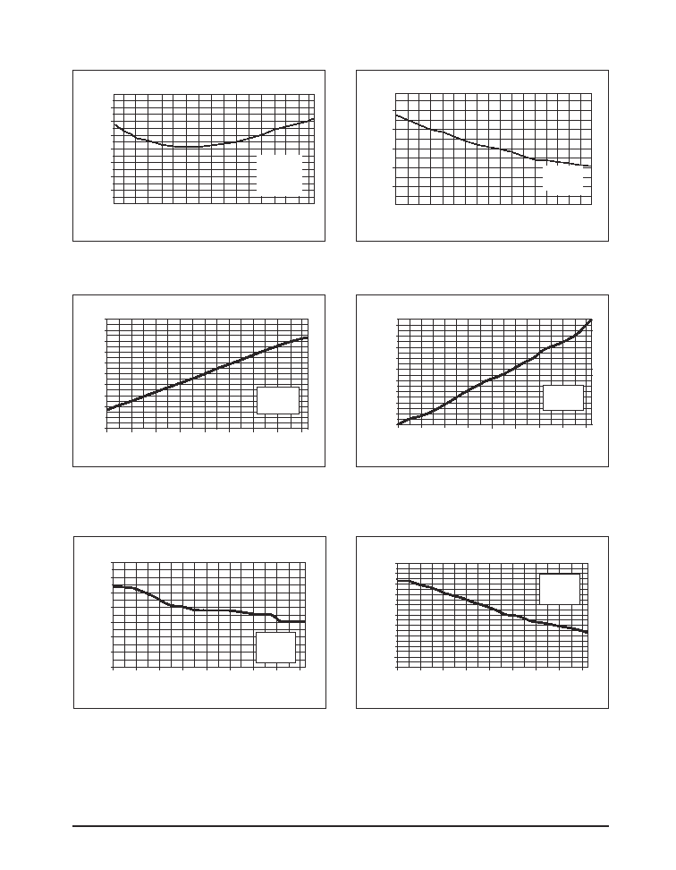
TYPICAL PERFORMANCE CHARACTERISTICS: Continued
Figure 6. Ground Current vs Load Current in Dropout
Figure 7. Dropout Voltage vs Load Current
Figure 8. Ground Current vs Temperature at
Figure 9. Output Voltage vs Temperature at
I
LOAD
= 10mA
I
LOAD
=10mA
100
90
80
70
60
50
40
30
20
10
0
3.3 Device
V
IN
= 3.2V
CL = 10
µ
F
0
0.25
0.5
0.75
1
1.25
1.5
IL(A)
I
GND
(mA)
280
270
260
250
240
230
220
210
200
190
180
-40
-20
0
20
40
60
80
100
120
I
GND
(
µ
A)
Temperature (
∞
C)
3.3V Device
V
IN
= 4.3V
IL = 10mA
CL = 10
µ
F
3.320
3.310
3.300
3.290
3.280
3.270
3.260
3.250
3.240
3.230
3.220
-40
-20
0
20
40
60
80
100
120
V
OUT
(V)
Temperature (
∞
C)
3.3V Device
V
IN
= 4.3V
IL = 10mA
CL = 10
µ
F
Figure 10. Ground Current vs Temperature at
Figure 11. Ground Current vs Temperature in Dropout
I
LOAD
=500mA
at I
LOAD
=750mA
600
500
400
300
200
100
0
0
0.25
0.5
0.75
1
1.25
1.5
V Dropout (mV)
IL (A)
3.3V Device
CL = 10
µ
F
7.00
6.80
6.60
6.40
6.20
6.00
5.80
5.60
5.40
5.20
5.00
-40
-20
0
20
40
60
80
100
120
I
GND
(mA)
Temperature (
∞
C)
3.3V Device
V
IN
= 4.3V
IL = 500mA
CL = 10
µ
F
30
29
28
27
26
25
24
23
22
21
20
-40
-20
0
20
40
60
80
100
120
I
GND
(mA)
Temperature (
∞
C)
3.3V Device
V
IN
= 3.2V
IL = 750mA
CL = 10
µ
F
5
Rev. 2/3/03 SPX3940 1A Low Dropout Voltage Regulator
© Copyright 2003 Sipex Corporation
TYPICAL PERFORMANCE CHARACTERISTICS: Continued
52.0
50.0
48.0
46.0
44.0
42.0
40.0
38.0
36.0
-40
-20
0
20
40
60
80
100
120
I
G
N
D
(m
A)
Temperature (
∞
C)
3.3V Device
V
IN
= 4.3V
IL=1.5A
CL = 10
µ
F
Figure 12. Ground Current vs Temperature at I
LOAD
= 1.5A
Figure 13. Ground Current vs Temperature in Dropout
at I
LOAD
=1.5A
100
95
90
85
80
75
70
-40
-20
0
20
40
60
80
100
120
I
G
N
D
m
A)
Temperature (
∞
C)
3.3V Device
V
IN
= 3.2V
IL = 1.5A
CL = 10
µ
F
350
330
310
290
270
250
230
210
190
170
150
-40
-20
0
20
40
60
80
Temperature (
∞
C)
V
DR
OPOUT
(mV)
120
100
3.3V Device
IL = 750mA
CL = 10
µ
F
Figure 14. Dropout Voltage vs Temperature at
I
LOAD
= 750mA
Figure 15. Dropout Voltage vs Temperature at
I
LOAD
= 1.5mA
Figure 16. Enable Current vs Temperature for V
EN
= 16V
2.00
1.90
1.80
1.70
1.60
1.50
1.40
1.30
1.20
1.10
1.00
-40
-20
0
20
40
60
80
Temperature (
∞
C)
V
TH
(V)
120
100
3.3V Device
V
IN
= 3.2V
IL = 750mA
CL = 10
µ
F
Figure 17. Enable Threshold vs Temperature
500
480
460
440
420
400
380
360
340
320
-40
-20
0
20
40
60
80
Temperature (
∞
C)
V
DR
OPOUT
(mV)
120
100
3.3V Device
IL = 1.5A
CL = 10
µ
F
35
30
25
20
15
10
5
0
-40
-20
0
20
40
60
80
Temperature (
∞
C)
I
EN
(
µ
A)
120
100
3.3V Device
V
IN
= 3.2V
IL = 750mA
CL = 10
µ
F