Rev. 12/19/00
1A Low Drop Out Voltage Regulator
with Shutdown
(PRELIMINARY INFORMATION)
FEATURES
APPLICATIONS
� Output Accuracy 3.3V, @ 1A Output
� Battery Powered Systems
� Very Low Quiescent Current
� Cordless Telephones
� Low Dropout Voltage
� Radio Control Systems
� Extremely Tight Load And Line Regulation
� Portable/Palm Top/Notebook Computers
� Very Low Temperature Coefficient
� Portable Consumer Equipment
� Current & Thermal Limiting
� Portable Instrumentation
� Error Flag Warns Of Output Dropout
� Automotive Electronics
� SMPS Post-Regulator
� Voltage Reference
PRODUCT DESCRIPTION
The SPX3940/41/42 is a low power voltage regulator. This device is an excellent choice for battery-powered applications such as
cordless telephones, radio control systems and portable computers. The SPX3940/41/42 features very low quiescent current (100
�A
Typ.) and very low dropout voltage. This includes a tight initial tolerance of 1% max and 2% max., and very low output temperature
coefficient, making the SPX3940/41/42 useful as a low-power voltage reference.
The error flag output feature is used as power-on reset for warning of a low output voltage, due to a falling voltage input of batteries.
Another feature is the logic-compatible shutdown input which enables the regulator to be switched on and off. The SPX3940/41/42 is
offered in 3-pin and 5-pin TO-220 package SOT-223, and surface mount TO-263 packages.
The regulator output voltage (of the 8-pin SO-8 and 5-pin TO-220 & TO-263) may be pin-strapped for a 3.3V or programmed from
1.24V to 29V with an external pair of resistors.
SPX3940
Front View
3
2
1
TO-263Package
V
OUT
GND/ ADJ
V
IN
SOT-223 Package
Front View
SPX3940
1
3
2
V
OUT
GND/
ADJ
V
IN
TO-263-5 Package
Top View
1 2 3 4 5
SPX3941/42
INPUT
GND
INPUT
ERROR
OUTPUT
GND
Five Lead Package Pin Functions:
1)
SPX3941
SPX3942
3)
4)
5)
ADJUST
SHUTDOWN
OUTPUT
SHUTDOWN
2)
Top View
SPX3941/42
TO-220-5 Package
5
4
3
2
1
TO-220 Package
Front View
SPX3940
V
OUT
GND/ ADJ
V
IN
Front View
TO-252 Package
3
2
1
SPX3940
ADJ/GND
V
IN
V
OUT
PIN CONNECTIONS
SPX3940/41/42
Rev. 12/19/00
SPX3940/41/42
ABSOLUTE MAXIMUM RATINGS
Power Dissipation..........................................Internally Limited
Input Supply Voltage ................................................... +7.5V
Lead Temp. (Soldering, 5 Seconds) ................................ 260�C
Feedback Input Voltage ..................................-1.5V to +30V
Storage Temperature Range .............................. -65� to +150�C
Shutdown Input Voltage..................................-0.3V to +30V
Operating Junction Temperature Range (Note 9)
Error Comparator Output ................................-0.3V to +30V
SPX3940/41/42...................................... -40C� to +125�C
ESD Rating ............................................................ 2KV Min
ELECTRICAL CHARACTERISTICS
at V
S
=�15V,T
A
=25�C, unless otherwise specified. Boldface applies over the full
operating temperature range.
PARAMETER
CONDITIONS
(Note 2)
Typ.
SPX3940A
Min Max
SPX3940/41
Min Max
UNITS
3.3V Version
Output Voltage
-
40
�C
T
J
+125�C
1mA
I
L
1A
3.3
3.3
3.267
3.217
3.333
3.382
3.234
3.185
3.366
3.415
V
All Voltage Options
Output Voltage
Temperature Coefficient
(Note 1)
20 100
150
ppm/�C
Line Regulation ( Note 3)
6V
V
IN
30V (Note 4)
20 40
60
mV
Load Regulation ( Note 3 )
I
L
= 50mA to 1mA
35
50
80
50
80
mV
Output Noise Voltage
BV = 10Hz � 100kHz
I
L
= 5mA
150
�V(rms)
Ground Current
4.5V<Vin<5.5V
I
L
= 5mA
Vin=5V
I
L
= 1A
10
110
15
20
200
250
15
20
200
250
mA
Current Limit
V
OUT
= 0
1.7
1.2
1.2
A
Thermal
Regulation
0.05 0.2 0.2 %/w
Dropout Voltage (Note 5)
I
L
= 1A
I
L
= 100mA
0.5
110
0.8
1.0
150
200
0.8
1.0
150
200
V
Adjustable Versions only
Typ
SPX3940/42
Reference Voltage
1.235
1.200
1.98
1.270
1.272
V
Reference Voltage
Over Temperature
(Note 6)
1.185
1.285 V
Feedback Pin Bias Current
20
60
80
nA
Reference Voltage
Temperature Coefficient
(Note 7)
50
ppm/�C
Feedback Pin Bias Current
Temperature Coefficient
0.1
nA/�C
Rev. 12/19/00
SPX3940/41/42
(Continued)
PARAMETER
CONDITIONS
(Note 2)
Typ. SPX3940/42
Min Max
UNITS
Output Leakage Current
V
0H
= 30V
0.01
1.00
2.00
�A
Output Low Voltage
V
IN
= 4.5V
I
0L
= 400
�A
150 250
400
mV
Upper Threshold Voltage
(Note 8)
60
40
25
mV
Lower Threshold Voltage
(Note 8)
75
95
140
mV
Hysteresis (Note
8)
15
mV
Input logic Voltage
Low (Regulator ON)
High (Regulator OFF)
1.3
2.0
0.7
V
Shut down Pin Input Current
V
S
= 2.4V
V
S
= 30V
30
450
90
150
800
1000
�A
Regulator Output Current in
Shutdown
3
15
25
�A
Note 1: Output or reference voltage temperature coefficients defined as the worst case voltage change divided by the total temperature range.
Note 2: Unless otherwise specified all limits are guaranteed for T
j
= 25
�C, V
IN
= 6V, I
L
= 100
�A and C
L
= 1
�F. Additional conditions for the 8-pin versions are
feedback tied to 5V tap and output tied to output sense (V
OUT
= 5V) and V
SHUTDOWN
0.8V.
Note 3: Regulation is measured at constant junction temperature, using pulse testing with a low duty cycle. Changes in output voltage due to heating effects are
covered under the specification for thermal regulation.
Note 4: Line regulation for the SPX3940/41/42 is tested at 150
�C for I
L
= 1 mA. For I
L
= 100
�A and T
J
= 125
�C, line regulation is guaranteed by design to 0.2%. See
typical performance characteristics for line regulation versus temperature and load current.
Note 5: Dropout voltage is defined as the input to output differential at which the output voltage drops 100 mV below its nominal value measured at 1V differential at
very low values of programmed output voltage, the minimum input supply voltage of 2V ( 2.3V over temperature) must be taken into account.
Note 6: V
REF
V
OUT
(Vin - 1V), 2.3 Vin30V, 100�AI
L
250 mA, T
J
T
JMAX
.
Note 7: Comparator thresholds are expressed in terms of a voltage differential at the feedback terminal below the nominal reference voltage measured at 6V input. To
express these thresholds in terms of output voltage change, multiply by the error amplifier gain = V
OUT
/V
REF
= (R1 + R2)/R2. For example, at a programmed output
voltage of 5V, the Error output is guaranteed to go low when the output drops by 95 mV x 5V/1.235 = 384 mV. Thresholds remain constant as a percent of V
OUT
as
V
OUT
is varied, with the dropout warning occurring at typically 5% below nominal, 7.5% guaranteed.
Note 8: V
SHUTDOWN
2V, V
IN
30V, V
OUT
=0, Feedback pin tied to 5V Tap.
Note 9: The junction -to-ambient thermal resistance of the TO-92 package is 180
�C/ W with 0.4" leads and 160�C/ W with 0.25" leads to a PC board.
The thermal resistance of the 8-Pin DIP package is 105
�C/W junction-to-ambient when soldered directly to a PC board. Junction-to-ambient thermal resistance for the
SOIC (S) package is 160
�C/W.
Rev. 12/19/00
SPX3940/41/42
APPLICATION HINTS
EXTERNAL CAPACITORS
The stability of the SPX3940/41/42 requires a 2.2
�F or greater
capacitor between output and ground. Oscillation could occur
without this capacitor. Most types of tantalum or aluminum
electrolytic works fine here. For operations of below -25
�C solid
tantalum is recommended since the many aluminum types have
electrolytes the freeze at about -30
�C. The ESR of about 5 or
less and resonant frequency above 500kHz are the most
important parameters in the value of the capacitor. The capacitor
value can be increased without limit.
At lower values of output current, less output capacitance is
required for stability. For the currents below 10mA the value of
the capacitor can be reduced to 0.5
�F and 0.15�F for 1A. More
output capacitance needed for the 8-pin version at voltages below
5V since it runs the error amplifier at lower gain. At worst case
5
�F or greater must be used for the condition of 250mA load at
1.23V output.
The SPX3940/41/42, unlike other low dropout regulators will
remain stable and in regulation with no load in addition to the
internal voltage divider. This feature is especially important in
application like CMOS RAM keep-alive. When setting the output
voltage of the SPX3940/41/42, a minimum load of 10mA is
recommended.
If there is more than 10 inches of wire between the input and the
AC filter capacitor or if a battery is used as the input then a 0.1
�F
tantalum or aluminum electrolytic capacitor should be placed
from the input to the ground.
Instability can occur if there is stray capacitance to the
SPX3940/41/42 feedback terminal (pin 7). This could cause
more problems when using a higher value of external resistors to
set the output voltage.
This problem can be fixed by adding a 100pF capacitor between
output and feedback and increasing the output capacitor to at least
3.3
�F.
ERROR DETECTION COMPARATOR OUTPUT
The Comparator produces a logic low output whenever the
SPX3940/41/42 output falls out of regulation by more than around
5%. This is around 60mV offset divided by the 1.235 reference
voltage. This trip level remains 5% below normal regardless of the
programmed output voltage of the regulator. Figure 1 shows the
timing diagram depicting the ERROR signal and the regulator output
voltage as the SPX3940/41/42 input is ramped up and down. The
ERROR signal becomes low at around 1.3V input, and goes high
around 5V input (input voltage at which Vout = 4.75). Since the
SPX3940/41/42's dropout voltage is load dependent, the input voltage
trip point (around 5V) will vary with the load current. The output
voltage trip point (approx. 4.75V) does not vary with load.
The error comparator has an open-collector output, which requires an
external pull-up resistor. Depending on the system requirements the
resistor may be returned to 5V output or other supply voltage. In
determining the value of this resistor, note that the output is rated to
sink 400
�A, this value adds to battery drain in a low battery
condition. Suggested values range from 100K to 1M
. If the output
is unused this resistor is not required.
PROGRAMMING THE OUTPUT VOLTAGE OF
SPX3940/41/42
The SPX3940/41/42 may be pin-strapped for 5V using its internal
voltage divider by tying Pin 1 (output) to Pin 2 (sense) and Pin 7
(feedback) to Pin 6 (5V Tap).
+
+
+
+
4 .7 5 V
O U T PU T
V O L T A G E
E R R O R *
_ _ _ _ _ _ _
IN P U T
V O L T A G E
1 .3 V
5 .0 V
F ig u r e 1 . E R R O R O u tp u t T im in g
_ _ _ _ _ _ _
* S e e A p p lica tio n In fo .
Rev. 12/19/00
SPX3940/41/42
Also, it may be programmed for any output voltage between its
1.235V reference and its 30V maximum rating. As seen in
Figure 2, an external pair of resistors is required.
Refer to the below equation for the programming of the output
voltage::
V
OUT
= V
REF
� ( 1 + R
1
\ R
2
)+ I
FB
R
1
The V
REF
is 1.235 and I
FB
is the feedback bias current, nominally
-20nA. The minimum recommended load current of 1
�A forces
an upper limit of 1.2 M
on value of R
2
.
If no load is presented
the I
FB
produces an error of typically 2% in V
OUT
, which may be
eliminated at room temperature by trimming R
1
. To improve the
accuracy choose the value of R2 = 100k this reduces the error by
0.17% and increases the resistor program current by 12
�A. Since
the LP2951 typically draws 60
�A at no load with Pin 2 open-
circuited this is a small price to pay
REDUCING OUTPUT NOISE
It may be an advantage to reduce the AC noise present at the output.
One way is to reduce the regulator bandwidth by increasing the size of
the output capacitor. This is the only way that noise can be reduced
on the 3 lead SPX3940/41/42 but is relatively inefficient, as
increasing the capacitor from 1
�F to 220�F only decreases the noise
from 430
�V to 160�V Vrms for a 100kHz bandwidth at 5V output.
Noise could also be reduced fourfold by a bypass capacitor across R
1
,
since it reduces the high frequency gain from 4 to unity. Pick
C
BYPASS
1 / 2R
1
� 200 Hz
or choose 0.01
�F. When doing this, the output capacitor must be
increased to 3.3
�F to maintain stability. These changes reduce the
output noise from 430
�V to 100�V Vrms for a 100kHz bandwidth at
5V output. With the bypass capacitor added, noise no longer scales
with output voltage so that improvements are more dramatic at higher
output voltages.
HEAT SINK REQUIREMENTS
Depending on the maximum ambient temperature and maximum
power dissipation a heat sink may be required with the
SPX3940/41/42. The junction temperature range has to be within
the range specified under Absolute Maximum Ratings under all
possible operating conditions. To find out if a heat sink is
required, the maximum power dissipation of the device needs to
be calculated. This is the maximum specific AC voltage that
must be taken into consideration at input. Figure 3 shows the
condition and power dissipation which should be calculated with
the following formula:
P
TOTAL
= (V
IN
- 5) I
L
+ (V
IN
)I
G
Next step is to calculate the temperature rise T
R
(max). T
J
(max)
maximum allowable junction temperature, T
A
(max) maximum
ambient temperature :
T
R
(max) = T
J
(max) - T
A
(max)
Junction to ambient thermal resistance
(j-A)
can be calculated
after determining of P
TOTAL &
T
R
(max):
(J-A)
= T
R
(max)/P
(max)
If the
(J-A)
is 60
�C/W or higher, the device could be operated
without a heat sink. If the value is below 60
�C/W then the heat
sink is required and the thermal resistance of the heat sink can be
calculated by the following formula,
(J-C)
junction to case,
(C-H)
case to heat sink,
(H-A)
heat sink to ambient:
(J-A)
=
(J-C)
+
(C-H)
+
(H-A)
+
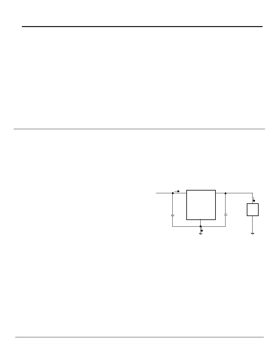
2.2 uF
+
SPX3940
I
IN
V
IN
I
G
I
L
3.3V
IN
OUT
GND
LOAD
I
IN
= I
L
+ I
G
Figure 3. 3.3V Regulator Circuit