 | –≠–ª–µ–∫—Ç—Ä–æ–Ω–Ω—ã–π –∫–æ–º–ø–æ–Ω–µ–Ω—Ç: SPX431S | –°–∫–∞—á–∞—Ç—å:  PDF PDF  ZIP ZIP |
Rev. 10/30/00
SPX431
Precision Adjustable Shunt Regulator
FEATURES
APPLICATIONS
∑ Trimmed Bandgap to 0.5%
∑ Battery Operating Equipments
∑ Wide Operating Current..........................1mA to 150mA
∑ Adjustable Supplies
∑ Extended Temperature Range....................0∞∞∞∞C to 105∞∞∞∞C
∑ Switching Power Supplies
∑ Low Temperature Coefficient ............................30 ppm/∞C
∑ Error Amplifiers
∑ Offered in TO-92, SOIC, SOT-89, SOT-23-5
∑ Single Supply Amplifier
∑ Improved Replacement in Performance for TL431
∑ Monitors / VCR / TV
∑ Low Cost Solution
∑ Personal Computers
PRODUCT DESCRIPTION
The SPX431 is a 3-terminal adjustable shunt voltage regulator providing a highly accurate 0.5% bandgap reference. SPX431 acts as an
open-loop error amplifier with a 2.5V temperature compensation reference. The SPX431 thermal stability, wide operating current
(150mA) and temperature range (0
∞C to 105∞C) makes it suitable for all variety of application that are looking for a low cost solution
with high performance. SPX431 tolerance of 0.5% is proven to be sufficient to overcome all of the other errors in the system to
virtually eliminate the need for trimming in the power supply manufactures assembly line and contribute a significant cost
savings.
The output voltage may be adjusted to any value between V
REF
and 36 volts with two external resistors. The SPX431 is operating an
extended temperature range of 0∞C to 105∞C. The SPX431 is available in TO-92, SO-8, SOT-89, and SOT-23-5 packages.
PIN CONFIGURATIONS
SOT-23-5 (M5)
3
2
1
Top View
SPX431
5
4
Top View
SPX431
SOT-89 (M1)
1
2
3
Bottom View
TO-92 (N)
1
3
2
N/C
REF
ANODE
CATHODE
CATHODE
ANODE
REF
Top View
2
1
3
4
8
7
6
5
SPX431
8-Pin Surface Mount (S)
CATHODE
REF
ANODE
ANODE
ANODE
ANODE
N/C
N/C
N/C CATHODE
ANODE
REF
Rev. 10/30/00
SPX431
ABSOLUTE MAXIMUM RATINGS
PARAMETER SYMBOL
RATING
UNITS
Cathode-Anode Reverse Breakdown
V
KA
37 V
Anode-Cathode Forward Current
I
AK
1 A
Operating Cathode Current
I
KA
150 mA
Reference Input Current
I
REF
10 mA
Continuous Power Dissipation at 25
∞ C
TO-92
SOT-23
8L SOIC
SOT-89
P
D
775
200
750
1000
mW
mW
mW
mW
Junction Temperature
T
J
150 ∞C
Storage Temperature
T
STG
- 65 to 150
∞C
Lead Temperature (Soldering 10 sec.)
T
L
300 ∞C
Stresses greater than those listed under ABSULUTE MAXIMUM RATINGS may cause permanent damage to the device. This is a stress rating only and functional
operation of the device at these or any other conditions above those indicated in the operational sections of this specification is not implied. Exposure to absolute
maximum rating conditions for extended periods may affect reliability.
RECOMMENDED CONDITIONS TYPICAL THERMAL RESISTANCES
PARAMETER SYMBOL
RATING
UNIT
PACKAGE 0
JA
0
JC
TYPICAL
DERATING
Cathode Voltage
V
KA
V
REF
to 20
V
TO-92
160
∞C/W 80
∞C/W 6.3
mW/
∞C
Cathode Current
I
K
10
mA
SOT-23
575
∞C/W 150
∞C/W 1.7
mW/
∞C
SOIC
175
∞C/W 45
∞C/W 5.7
mW/
∞C
SOT-89
110
∞C/W 8
∞C/W 9.1
mW/
∞C
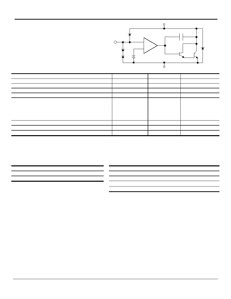
2.5V
+
-
REFERENCE
(R)
CATHODE (K)
ANODE (A)
Rev. 10/30/00
SPX431
ELECTRICAL CHARACTERISTICS
at 25∞C I
K
@ 10mA V
K
= V
REF
,
unless otherwise specified.
Parameter
Symbol
Test Conditions
Test Circuit
SPX431
Unit
Min Typ Max
Reference Voltage
V
REF
T
A
= 25
∞C
Over Temp.
1
1
2.490
2.469
2.503 2.515
2.536
V
V
V
REF
with Temp.
TC 1
0.07
0.20
mV/
∞C
Ratio of Change in V
REF
to
Cathode Voltage
V
REF
V
K
V
REF
to 10V
10V to 36V
2
-2.7
-2
-1.0
-0.4
0.3
mV/V
Reference Input Current
I
REF
2
0.7
4
µA
I
REF
Temp Deviation
I
REF
Over Temp.
2
0.4
1.2
µA
Min I
K
for Regulation
I
K(MIN)
1
0.4
1
mA
Off State Leakage
I
K(OFF)
V
REF
= 0V,
V
KA
= 36V
3
0.04
250 nA
Dynamic Output Impedance
Z
KA
1
0.15
0.5
TC = Test Circuit
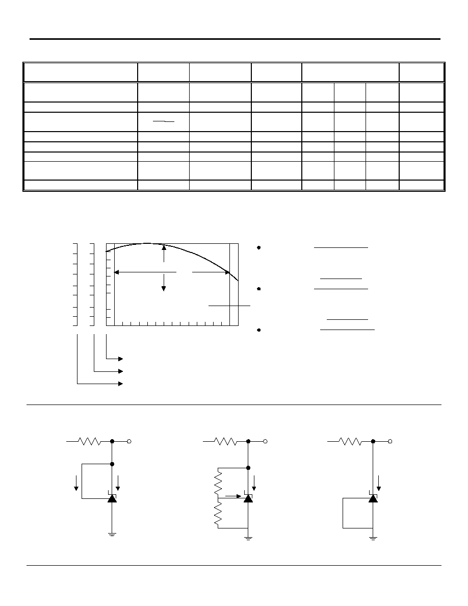
Calculating Average Temperature Coefficient (TC)
TEST CIRCUITS
ppm
mV
TC in mV/∞C =
V
REF
(mV)
T
A
TC in %/∞C =
V
REF
at 25∞C
T
A
V
REF
)
)
x 100
TC in ppm/∞C =
V
REF
at 25∞C
T
A
V
REF
)
)
x 10
6
5000
-55
0.06 mV/∞C
V
REF
0
0
0
%
-20
-10
0.5
Temperature (∞C)
0.002 %/∞C
24 ppm/∞C
-25
0
25
50
75 100 125
I
K
I
REF
V
IN
V
KA
= V
REF
V
IN
V
KA
I
K
R
1
R
2
(V
REF
)
Figure 1b. Test Circuit 2
Figure 1a. Test Circuit 1
V
IN
V
KA
I
K (OFF)
Figure 1c. Test Circuit 3
I
REF
Rev. 10/30/00
SPX431
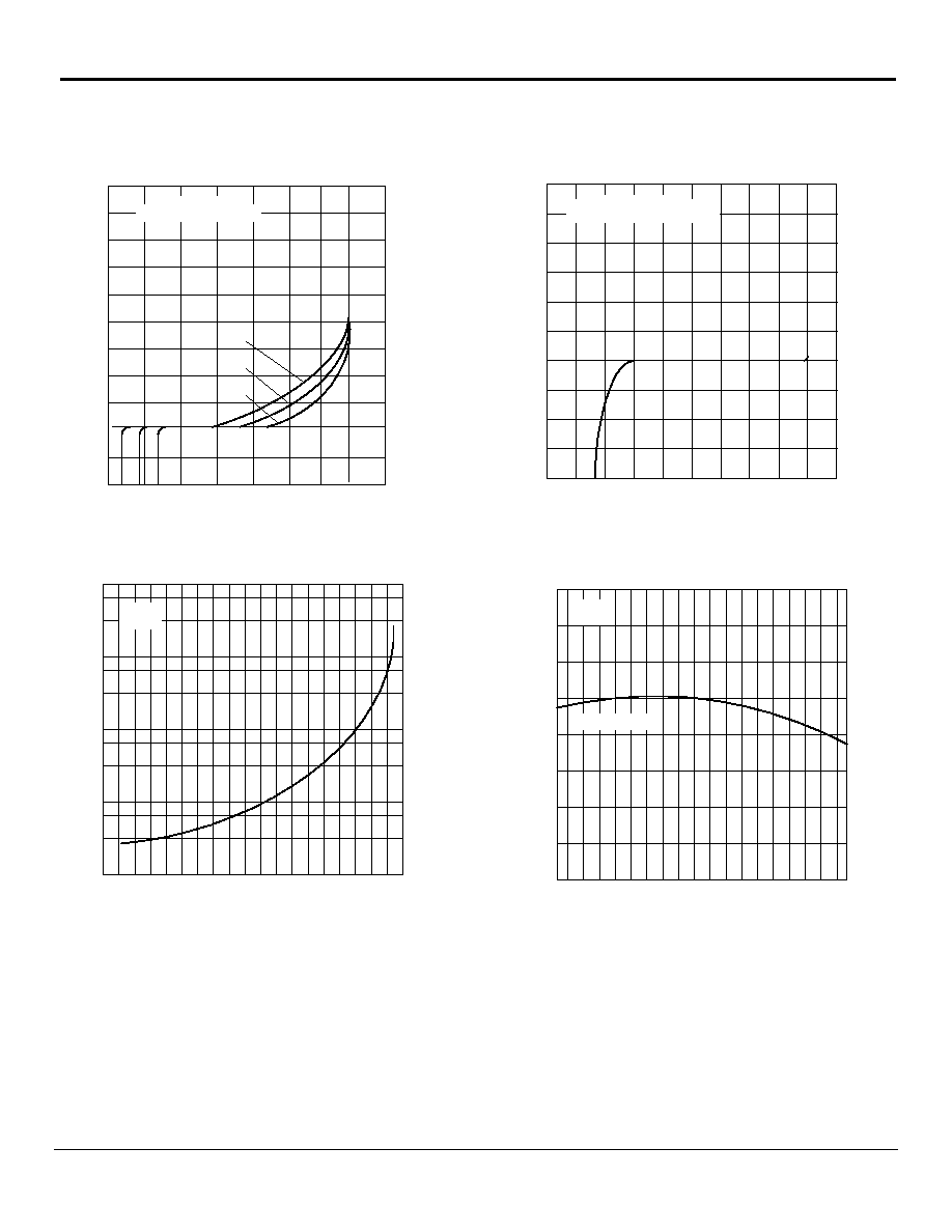
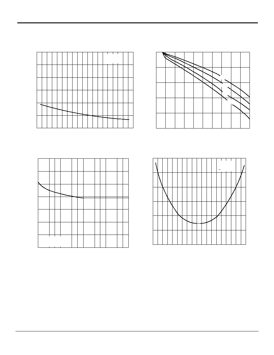
TYPICAL PERFORMANCE CURVES
V
R
EF
- Reference Voltage (V)
V
KA
- Cathode Voltage (V)
High Current Operating Characteristics
Figure 3
-2
-1
0
1
2
3
-100
-75
-50
-25
0
25
50
75
100
125
150
I
K
- Cathode Current (mA)
V
KA
= V
REF
Temperature Range: - 0∞C to 105 ∞C
Figure 4
Off State Leakage
-60
-30
0
30
60
90
120
0.01
0.1
1
10
100
T
A
- Ambient Temperature ( ∞C)
I
Z
off - Off State Cathode Current (nA)
V
KA
= 36V
V
REF
= 0V
Figure 5
T
A
- Ambient Temperature ( ∞C)
90
120
Reference Voltage vs. Ambient Temperature
-60
-30
0
30
60
2.45
2.46
2.47
2.48
2.49
2.50
2.51
2.52
2.53
V
KA
= V
REF
I
K
= 10 mA
V
REF
= 2.500 V at 25 ∞C
Figure 2
Low Current Operating Characteristics
V
KA
- Cathode Voltage (V)
900
800
700
600
500
400
300
200
100
0
-100
-200
1.0
-1.0
2.0
0
3.0
I
K
- Cathode Current (
µ
µ
µ
µ
A)
V
KA
= V
REF
Temperature Range: -0∞C to 125 ∞C
105 ∞C
25 ∞C
-0 ∞C
Rev. 10/30/00
SPX431
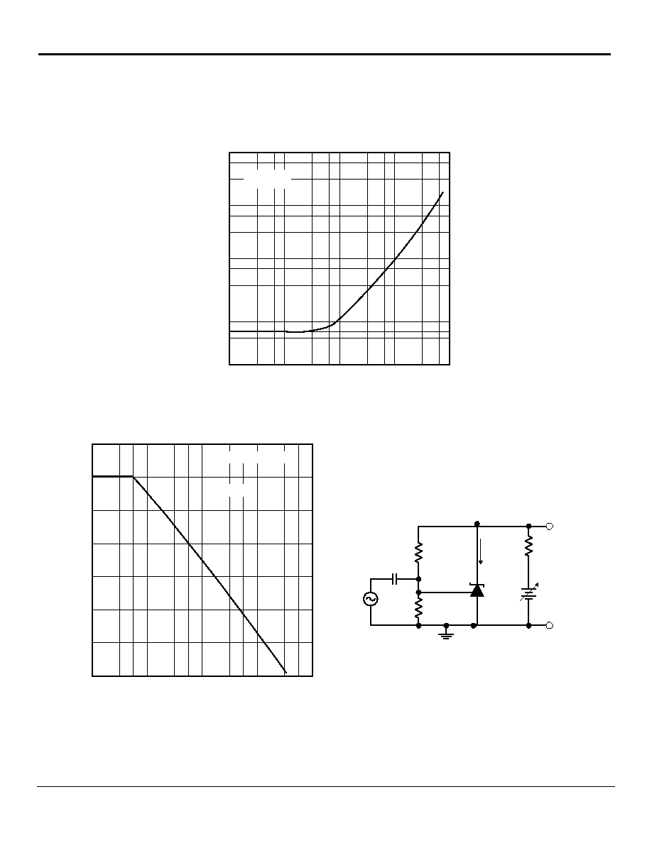
TYPICAL PERFORMANCE CURVES
30
Figure 8
f - Frequency (Hz)
Noise Voltage nV/
Hz
20
10
10
100
1 k
10 k
100 k
0
Noise Voltage
70
30
40
50
60
V
KA
= V
REF
I
K
= 10 mA
T
A
= 25∞C
T
A
- Free Air Temperature
Figure 9
Low Frequency Dynamic Output Impedance
Z
K
A
- Dynamic Impedance (
)
-60
-30
0
30
60
90
120
0.0
V
KA
= V
REF
I
KA
= 1 to 100 mA
f < 1 kHz
0.025
0.050
0.075
0.100
0.125
0.150
Figure 7
Reference Voltage Line Regulation
V
KA
- Cathode Voltage (V)
V
KA
- Cathode Voltage (V)
0
-10
-20
-30
-40
-50
0
3
6
9
12
15
18
21
24
27
105 ∞C
75 ∞C
25 ∞C
0 ∞C
T
A
- Ambient Temperature ( ∞C)
Figure 6
Reference Input Current
I
R
EF
- Reference Input Current (
µ
µ
µ
µ
A)
-60
-30
0
30
60
90
120
0
R1 = 10 k
R2 =
I
K
= 10 mA
0.5
1.0
1.5
2.0
2.5
3.0
Rev. 10/30/00
SPX431
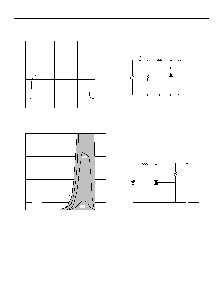
TYPICAL PERFORMANCE CURVES
Figure 11
10 M
Dynamic Output Impedance
Figure 10
f - Frequency (Hz)
Z
KA
- Dynamic Impedance
100
0.1
1.0
10
1 k
10 k
100 k
1 M
0.01
T
A
= 25 ∞C
I
K
= 1 to 100 mA
9
µF
15 k
8.25 k
GND
OUT
230
I
K
Small Signal Voltage Gain vs. Frequency
f - Frequency (Hz)
A
V
- Small Signal Voltage Gain (dB)
70
20
30
40
10
50
60
1 k
10 k
100 k
1 M
10 M
0
Temperature Range: -0∞C to 105 ∞C
I
K
= 10 mA
Rev. 10/30/00
SPX431
TYPICAL PERFORMANCE CURVES
OUT
GND
220
f
P
= 100 kHz
INPUT
MONITOR
50
Pulse Response
Figure 12
t - Time (
µ
µ
µ
µs)
Input and Output Voltages (V)
12
-1
0
1
2
3
4
5
6
11
10
9
8
7
6
5
4
3
2
1
0
150
10 k
I
K
C
L
Stability Boundary Conditions
Figure 13
C
L
- Load Capacitance (pF)
I
K
- Cathode Current (mA)
OUTPUT
INPUT
10
7
10
6
10
5
10
4
10
3
10
2
10
1
10
0
0
10
20
30
40
50
60
70
80
90
100
STABILITY
REGION
T
A
= 25 ∞C
A: V
KA
= V
REF
B: V
KA
= 5V at I
K
= 10 mA
C: V
KA
= 10V at I
K
= 10 mA
D: V
KA
= 15V at I
K
= 10 mA
D
C
A
B
Rev. 10/30/00
SPX431
ORDERING INFORMATION
Ordering No. Precision Output Accuracy
Packages
SPX431M5
0.5%
2.5V
5 Lead SOT-23
SPX431M1
0.5%
2.5V
5 Lead SOT-89
SPX431S
0.5%
2.5V
8 Lead SOIC
SPX431N
0.5%
2.5V
3 Lead TO-92
SIGNAL PROCESSING EXCELLENCE
Sipex Corporation
Headquarters and Main Offices:
22 Linnell Circle
Billerica, MA 01821
TEL: (978) 667-8700
FAX: (978) 670-9001
e-mail: sales@sipex.com
233 South Hillview Drive
Milpitas, CA 95035
TEL: (408) 935-7600
FAX: (408) 934-7500
Sipex Corporation reserves the right to make changes to any products described herein. Sipex does not assume any liability arising out of the application or use of any product or circuit described
hereing; neither does it convey any license under its patent rights nor the rights of others.
Corporation