 | –≠–ª–µ–∫—Ç—Ä–æ–Ω–Ω—ã–π –∫–æ–º–ø–æ–Ω–µ–Ω—Ç: SPX432A | –°–∫–∞—á–∞—Ç—å:  PDF PDF  ZIP ZIP |
1
Rev. 2/21/03 SPX432 1.24V Precision Adjustable Shunt Regulator
© Copyright 2003 Sipex Corporation
1.24V Precision Adjustable Shunt Regulator
SPX432
DESCRIPTION
FEATURES
Low Voltage Operation, 1.24V
Trimmed Bandgap to 0.5% and 1%
Wide Operating Current, 1mA to 80mA
Adjustable Output Voltage, V
REF
to 18V
Extended Temperature Range:
0
∞
C to 105
∞
C
Low Temperature Coefficient, 50 ppm/
∞
C
Offered in TO-92, SOIC, SOT-23-3
Replacement for TLV431, AS432
Æ
The SPX432 is a 3-terminal adjustable shunt voltage regulator providing a highly accurate 1.24V
bandgap reference with 0.5% tolerance. The SPX432's thermal stability, wide operating current
(80mA) and temperature range (0
∞C to 105∞C) makes it suitable for a variety of applications. SPX432
tolerance of 0.5% is proven to be sufficient to overcome all of the other errors in the system to virtually
eliminate the need for trimming in the power supply manufactures' assembly lines and contribute a
significant cost savings.
The SPX432 is an ideal voltage reference in an isolated feedback circuit for switch mode power
supplies. SPX432 offers many advantages over the TLV431 such as wider output voltage (18V vs.
6V), higher output current (80mA vs. 15mA) and a wider operating temperature range with a tighter
tolerance down to 0.5%.
APPLICATIONS
Switching Power Supplies
Adjustable Supplies
Error Amplifiers
Single Supply Amplifier
Monitors / VCRs / TVs
Personal Computers
Voltage References
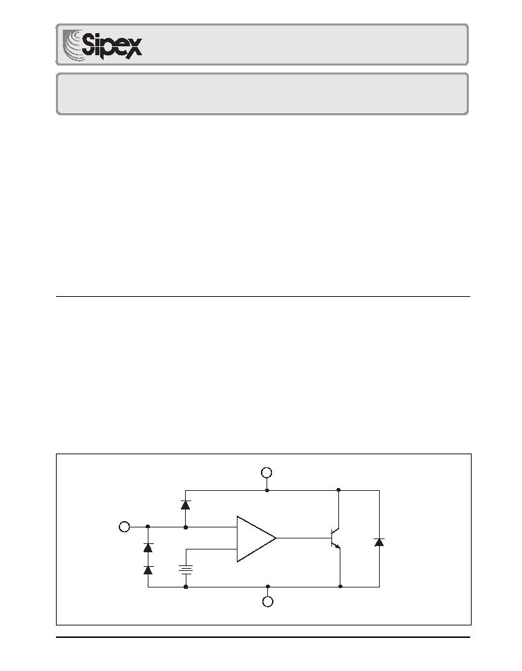
BLOCK DIAGRAM
Cathode (K)
1.24V
Reference
(R)
+
-
Anode (A)
2
Rev. 2/21/03 SPX432 1.24V Precision Adjustable Shunt Regulator
© Copyright 2003 Sipex Corporation
ABSOLUTE MAXIMUM RATINGS
Cathode-Anode Reverse Breakdown V
KA
....................................... 20V
Anode-Cathode Forward Current, (<10ms) I
AK
................................. 1A
Operating Cathode Current I
KA
.................................................... 80mA
Reference Input Current I
REF
.......................................................... 1mA
Continuous Power Dissipation at 25
∞
C P
D
TO-92 ..................................................................... 775mW
SOT-23 .................................................................. 200 mW
SOIC-8 .................................................................... 750mW
Junction Temperature T
J
........................................................... 150
∞
C
Storage Temperature T
STG
.......................................... -65
∞
C to 150
∞
C
Lead Temperature (Soldering 10 sec.) T
L
.................................. 300
∞
C
Stresses greater than those listed under ABSOLUTE MAXIMUM RATINGS may cause permanent damage to the device. This is a stress rating only
and functional operation of the device at these or any other conditions above those indicated in the operational sections of this specification is not
implied. Exposure to absolute maximum rating conditions for extended periods may affect reliability.
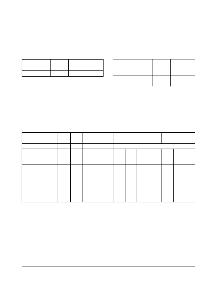
ELECTRICAL CHARACTERISTICS
Electrical characteristics are guaranted over the full junction temperature range (0
∞C to 105∞C). Ambient temperature must
be derated based upon power dissipation and package thermal characteristics. Unless otherwise specified, test conditions are:
V
KA
= V
REF
and I
K
= 10mA.
PARAMETER
SYMBOL
TEST
CONDITIONS
MIN
TYP
MAX
MIN
TYP
MAX
UNITS
CIRCUIT
SPX432A
SPX432
Output Voltage
V
REF
3a
1.2338
1.240
1.2462
1.2276
1.240
1.2524
V
Temperature Deviation
V
REF
3a
0 < T
J
< 105
∞
C
12
20
12
20
mV
Line Regulation
V
REF
3b
V
KA
= 1.25V to 15V
19
37
19
37
mV
Load Regulation
V
REF
3a
I
K
= 1mA to 80mA
12
30
12
30
mV
Reference Input Current
I
REF
3b
3
6
3
6
µ
A
Reference Input Current
I
REF
3b
0 < T
J
< 105
∞
C,
0.3
0.6
0.3
0.6
µ
A
Temperature Coefficient
Minimim Cathode
I
K(MIN)
3a
0.6
1
0.6
1
mA
Current for Regulation
Off State Leakage
I
K(MIN)
3c
V
REF
= 0V,
0.04
500
0.04
500
nA
V
KA
= 18V
RECOMMENDED CONDITIONS
PARAMETER
SYMBOL
RATING
UNIT
Cathode Voltage
V
KA
V
REF
to 18
V
Cathode Current
I
K
10
mA
TYPICAL THERMAL RESISTANCES
PACKAGE
0
JA
0
JC
TYPICAL
DERATING
TO-92
160
∞
C/W
80
∞
C/W
6.3mW/
∞
C
SOT-23
575
∞
C/W
150
∞
C/W
1.7 mW/
∞
C
SOIC-8
175
∞
C/W
45
∞
C/W
5.7mW/
∞
C
Typical deratings of the thermal resistances are given for ambient
temperature >25
∞
C.
3
Rev. 2/21/03 SPX432 1.24V Precision Adjustable Shunt Regulator
© Copyright 2003 Sipex Corporation
0
5000
ppm
0
0.5
%
27ppm/
∞
C
0.0027% /
∞
C
0.0033mV /
∞
C
0
15
30
45
60
75
90
105
0
mV
-5
T
V
REF
Junction Temperature (
∞
C)
V
REF
(mV)
T
A
(
V
REF
at 25
∞
C
)
T
A
V
REF
x 100
∑
TC in % /
∞
C =
∑
TC in mV /
∞
C =
(
V
REF
at 25
∞
C
)
T
A
V
REF
x 10
6
∑
TC in ppm /
∞
C =
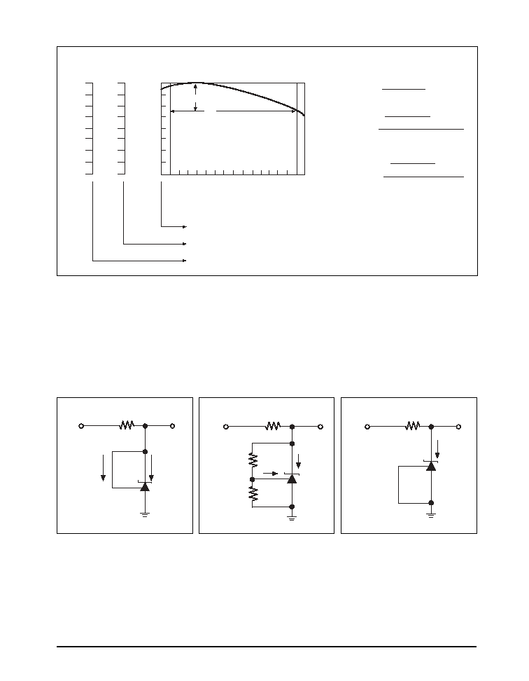
CALCULATION AVERAGE TEMPERATURE COEFICIENT (TC)
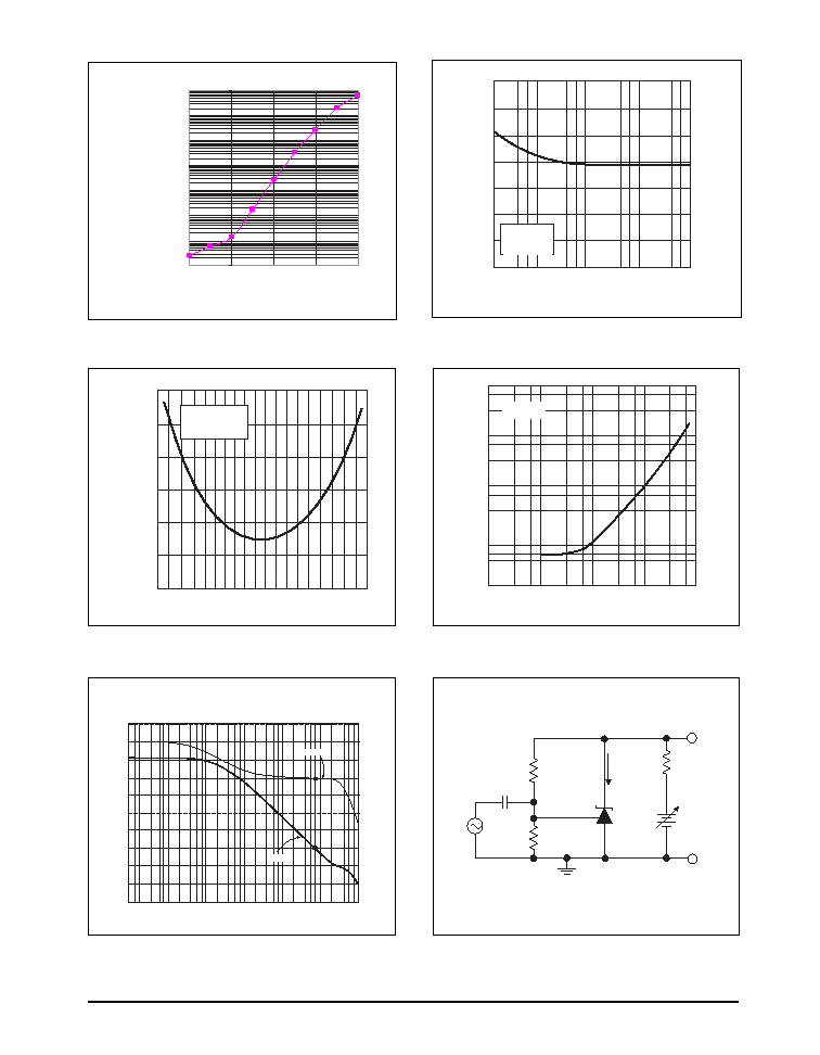
Figure 1. V
REF
VS Temperature.
TEST CIRCUITS
I
REF
V
KA =
V
REF
V
IN
I
K
I
REF
V
KA
V
IN
I
K
(V
REF
)
R1
R2
V
KA
V
IN
I
K (OFF)
Figure 2. Test Circuit for V
KA
= V
REF
Figure 3. Test Circuit for V
KA
> V
REF
Figure 4. Test Circuit for I
KOFF
4
Rev. 2/21/03 SPX432 1.24V Precision Adjustable Shunt Regulator
© Copyright 2003 Sipex Corporation
-2
-1
0
1
2
3
15.0
12.5
10.0
7.5
5.0
2.5
0
-2.5
-5.0
-7.5
-10.0
V
KA
Cathode Voltage (V)
I
K
Cathode Current (mA)
V
KA
= V
REF
0
∞
C to 105
∞
C
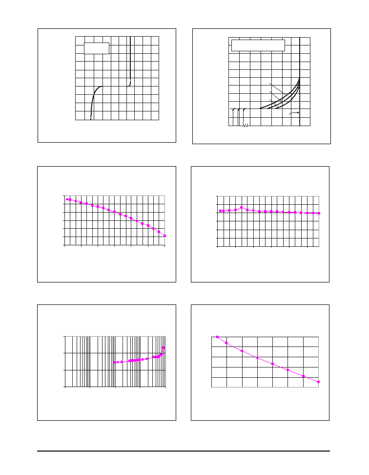
TYPICAL PERFORMANCE CHARACTERISTICS
900
800
700
600
500
400
300
200
100
0
-100
-200
-1.0
0
=
105 ∞C
25 ∞C
-0 ∞C
V
KA
- Cathode Voltage (V)
I
K
- Cathode Current (µA)
-0.5
0.25
0.5
0.75
1.0
1.25
1.5
1.24
V
KA
= V
REF
Temperature Range: 0
∞C to 105∞C
High Current Operating Characteristics.
V
KA
= V
REF,
I
KA
= 10mA.
Low Current Operating Characteristics.
V
KA
= V
REF,
Sweeping I
KA
, 25
∞C.
Reference Input Current VS Temperature; I
KA
= 10mA.
Reference Voltage Line Regulation; I
KA
= 10mA
,
Sweeping V
KA
, 25
∞C.
0
0.5
1
1.5
2
2.5
3
-60
-30
0
30
60
90
T
A
-Ambient Temperature (C)
I
REF
-Reference Input Current
(uA)
1.235
1.24
1.245
1.25
0.01
0.1
1
10
100
I
K
--cathode Current (mA)
V
KA
--Cathode V
oltage (V)
1.22
1.225
1.23
1.235
1.24
1.245
1.25
-60
-30
0
30
60
90
120
T
A
-Ambient Temperature (C)
V
REF
-Reference V
oltage (V)
-50
-40
-30
-20
-10
0
0
3
6
9
12
15
18
21
V
KA
-Cathode Voltage (V)
dV
REF
(mV)
5
Rev. 2/21/03 SPX432 1.24V Precision Adjustable Shunt Regulator
© Copyright 2003 Sipex Corporation
10
100
1K
10K
100K
70
60
50
40
30
20
10
0
f Frequency (Hz)
Noise V
oltage nV/
Hz
V
KA
= V
REF
I
K
= 10mA
T
A
= 25
∞
C
-60
-30
0
30
60
90
120
0.150
0.125
0.100
0.075
0.050
0.025
0.0
T
A
Free Air Temperature
Z
KA
Dynamic Impedance (
)
V
KA
= V
REF
I
K
= 1 to 80mA
f
1kHz
10
100
1K
10K
100K
1M
10M
START 10.000Hz
STOP 10 000 000.000Hz
REF LEVEL
0.0deg
70.000dB
/DIV
45.000deg
10.000dB
MARKER 735
PHASE (A/R)
MARKER 735
MAG (A/R)
074.781Hz
87.012deg
074.781Hz
0.047dB
GAIN
PHASE
60dB
50dB
40dB
30dB
20dB
10dB
0dB
-10dB
-20dB
-30dB
215
∞
180
∞
135
∞
90
∞
45
∞
0
∞
-45
∞
-90
∞
-135
∞
-180
∞
-215
∞
70dB
Off State Leakage; V
KA
= 18V, V
REF
= 0V.
Noise Voltage VS Frequency.
TYPICAL PERFORMANCE CHARACTERISTICS Continued:
10
µF
15k
3.03k
GND
230
I
K
V
IN
V
OUT
Low Frequency Dinamic Output Impedance VS T
AMBIENT
.
Small Signal Gain and Phase VS Frequency; I
K
= 10mA,
T
A
= 25
∞C.
Test Circuit for Gain and Phase Frequency Response.
0.0001
0.0010
0.0100
0.1000
1.0000
10.0000
100.0000
1000.0000
-50
0
50
100
150
T
A
Ambient Temperature (C)
I
KOFF
Cathode Current (nA)
100
0.1
1.0
10
1 k
10 k
100 k
1 M
0.01
T
A
= 25
∞C
I
K
= 1 to 80 mA
Z
KA
- Dynamic Impedance (
)
f - Frequency (Hz)
10 M
Dynamic Output Impedance T
A
= 25
∞C, I
KA
= 1 to 80mA.