1
Rev. 9/22/03 SPX5205 150mA, Low Noise LDO Voltage Regulator
© Copyright 2003 Sipex Corporation
150mA, Low-Noise LDO Voltage Regulator
SPX5205
DESCRIPTION
FEATURES
Low Noise Output LDO: 40µV
RMS
Possible
1% Initial Accuracy
Very Low Quiecent Current: 70µA
Low Dropout Voltage (210mV at 150mA)
Current and Thermal Limiting
Reverse-Battery Protection
Wide Range of Fix Output Voltages: 1.5V, 1.8V,
2.0V, 2.5V, 2.8V, 3.3V and 5.0V
Zero Off-Mode Current
Small 5-Pin SOT-23
Pin Compatible to MIC5205/MAX8877
(fixed Options Only) and AS3815
Æ
The SPX5205 is a positive voltage regulator with very low dropout voltage, output noise and ground current
(750µA at 100mA). V
OUT
has a tolerance of less than 1% and is temperature compensated. Fixed output
voltages 1.5V, 1.8V, 2.0V, 2.5V, 2.8V, 3.3V, and 5.0V and an adjustable version are available in a small
5-pin SOT-23 package. Other key features include zero off-mode current, reverse battery protection,
thermal shutdown and current limit. The SPX5205 is an excellent choice for use in battery-powered
applications, and where powe
r conservation is desired such as: cellular/ cordless telephones, radio control systems,
and portable computers.
APPLICATIONS
PDA
Battery Powered Systems
Cellular Phone
Cordless Telephones
Radio Control Systems
Laptop, Palmtop, and Notebook Computers
Portable Consumer Equipment
Portable Instrumentation
Bar Code Scanners
SMPS Post-Regulator
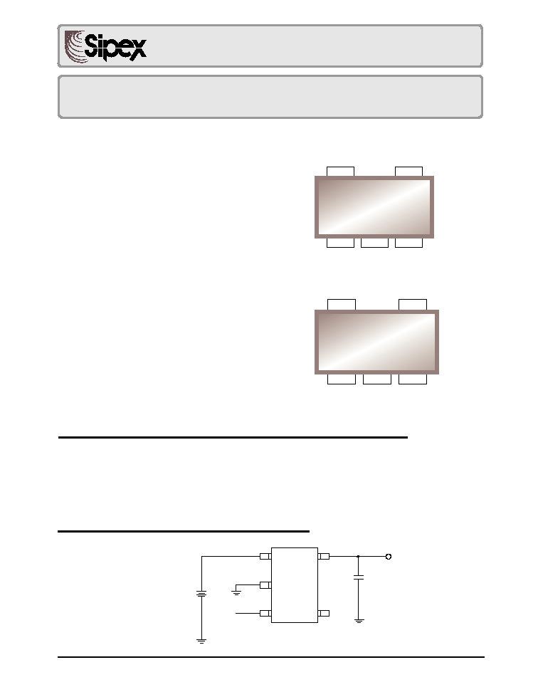
+
+
GND
EN
BYP
(Optn)
ENABLE may be tied directly to V
IN
SPX5205
1
2
3
4
5
V
IN
V
OUT
TOP View
1.0µF
TYPICAL APPLICATION CIRCUIT
5
4
1
2
3
SPX5205
5 Pin SOT-23
V
IN
BYP
GND
EN
V
OUT
5
4
1
2
3
SPX5205
5 Pin SOT-23
V
IN
ADJ/BYP
GND
EN
V
OUT
Fixed Output Voltage
Adjustable Output Voltage
2
Rev. 9/22/03 SPX5205 150mA, Low Noise LDO Voltage Regulator
© Copyright 2003 Sipex Corporation
Thermal Shutdown .................................................................... Internally Limited
Lead Temperature (Soldering, 5 seconds) ................................................. 260∞C
Operating Junction Temperature Range .................................... -40∞C to +125∞C
ELECTRICAL CHARACTERISTICS
T
J
=25∞C, V
IN
= V
OUT
+ 1V, I
L
= 100µA, C
L
= 1µF, and V
ENABLE
2.4V. The denotes the specifications which
apply over full temperature range -40∞C to +85∞C, unless otherwise specified.
PARAMETER
MIN
TYP
MAX
UNITS
CONDITIONS
Output Voltage Tolerance (V
OUT
)
-1
+1
%V
NOM
-2
+2
Output Voltage Temperature Coefficient
57
ppm/∞C
Line Regulation
0.03
0.1
%/V
V
IN
= V
OUT
+ 1V to 16V
0.2
Load Regulation
0.1
0.2
%
I
L
= 0.1mA to 150mA
0.5
Dropout Voltage (See Note 2)
30
50
mV
I
L
= 100µA
(V
IN
- V
O
)
70
140
190
mV
I
L
= 50mA
230
180
250
mV
I
L
= 100mA
300
210
275
mV
I
L
= 150mA
350
Quiescent Current (I
GND
)
0.05
1
µA
V
ENABLE
0.4V
5
V
ENABLE
0.25V
Ground Pin Current
70
125
µA
I
L
= 100µA
(I
GND
)
150
350
600
I
L
= 50mA
800
750
1000
I
L
= 100mA
1500
1300
1900
I
L
= 150mA
2500
Ripple Rejection (PSRR)
70
dB
Current Limit (I
LIMIT
)
360
500
mA
V
OUT
= 0V
Output Noise (e
NO
)
300
µV
RMS
I
L
= 10mA, C
L
= 1µF, C
IN
= 1µF
(10Hz - 100kHz.)
40
µV
RMS
I
L
= 10mA, C
L
= 10µF, C
BYP
=
1µF,C
IN
=1µF,(10Hz - 100kHz)
Input Voltage Level
0.4
V
OFF
Logic Low (V
IL
)
Input Voltage Level
2.0
ON
Logic High (V
IL
)
ENABLE Input Current
0.01
2
µA
V
IL
0.4V
3
20
V
IH
2.0V
ABSOLUTE MAXIMUM RATINGS
Input Supply Voltage ......................................... -20V to +20V
Enable Input Voltage ......................................... -20V to +20V
Input voltage ..................................................................................... +2.5V to 16V
Operating Junction Temperature Range .................................... -40∞C to +125∞C
Enable Input Voltage .............................................................................. 0V to V
IN
SOT-23-5 (
JA
) ................................................................................... See Note 1
RECOMMENDED OPERATING CONDITIONS
Note 1: The maximum allowable power dissipation is a function of maximum operating junction temperature, T
J (max)
, the junction to ambient thermal
resistance, and the ambient, J
A
, and the ambient temperature T
A
. The maximum allowable power dissipation at any ambient temperature is
given: P
D (max)
= (T
J (max)
- T
A
)/J
A
, exceeding the maximum allowable power limit will result in excessive die temperature; thus, the
regulator will go into thermal shutdown. The J
A
of the SPX5205 is 220∞C/W mounted on a PC board.
Note 2: Not applicable to output voltages of less than 2V.
3
Rev. 9/22/03 SPX5205 150mA, Low Noise LDO Voltage Regulator
© Copyright 2003 Sipex Corporation
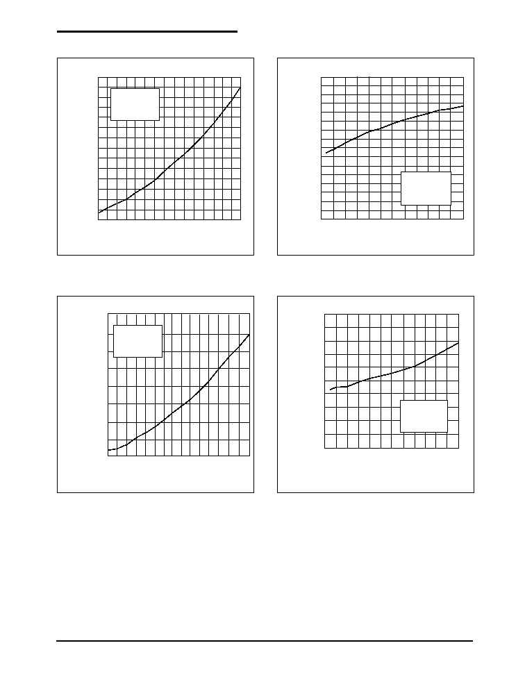
TYPICAL PERFORMANCE CHARACTERISTICS
Ground Current vs Load Current
Ground Current vs Input Voltage
1.40
1.20
1.00
0.80
0.60
0.40
0.20
0.00
0
50
100
150
I
L
(mA)
I
GND
(mA)
3.3V Device
V
IN
= 3.2V
C
L
= 1.0µF
110
100
90
80
70
60
50
40
30
4
6
8
10
12
14
16
V
IN
(V)
I
GND
(
µ
A)
V
O
= 3.3V
C
L
= 1.0µF
I
L
= 100µA
Ground Current vs Load Current in Dropout
Output Voltage vs Input Voltage
2.00
1.50
1.00
0.50
0.00
0
50
100
150
I
L
(mA)
I
GND
(mA)
3.3V Device
V
IN
= 4.3V
C
L
= 1.0µF
3.340
3.335
3.330
3.325
3.320
3.315
3.310
3.305
3.300
3.295
3.290
4
6
8
10
12
14
16
V
IN
(V)
V
OUT
(V)
3.3V Device
C
L
= 1.0µF
I
L
= 100µA
4
Rev. 9/22/03 SPX5205 150mA, Low Noise LDO Voltage Regulator
© Copyright 2003 Sipex Corporation
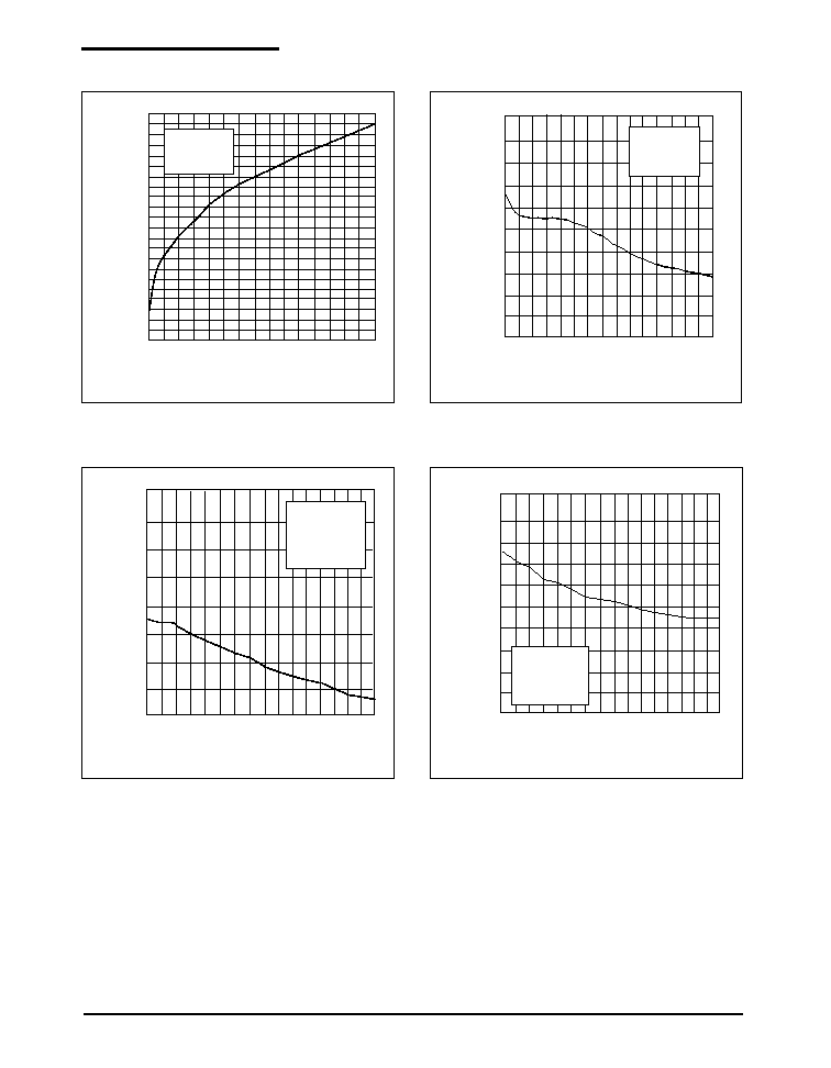
Dropout Voltage vs Load Current
Output Voltage vs Load Current
Ground Current vs Temperature at I
LOAD
=100
µA
Ground Current vs Temperature at I
LOAD
=100mA
200
150
100
50
0
0
50
100
150
I
L
(mA)
Dropout (mV)
V
O
=3.3V
V
IN
= 3.2V
C
L
= 1.0µF
3.310
3.308
3.306
3.304
3.302
3.300
0
50
100
150
I
L
(mA)
V
OUT
(V)
3.3V Device
V
IN
= 4.3V
C
L
= 1.0µF
90.0
80.0
70.0
60.0
50.0
-40
-20
0
20
40
60
80
100 120
Temperature (∞C)
I
GND
(
µ
A)
V
OUT
= 3.3V
V
IN
= 4.3V
C
L
= 1.0µF
I
L
= 100µA
950
850
750
650
550
450
-40
-20
0
20
40
60
80
100 120
Temperature (∞C)
I
GND
(
µ
A)
V
OUT
= 3.3V
V
IN
= 4.3V
C
L
= 1.0µF
I
L
= 100mA
TYPICAL PERFORMANCE CHARACTERISTICS: Continued
5
Rev. 9/22/03 SPX5205 150mA, Low Noise LDO Voltage Regulator
© Copyright 2003 Sipex Corporation
Ground Current in Dropout vs Temperature
Output Voltage vs Temperature
ENABLE Voltage, ON threshold vs Input Voltage
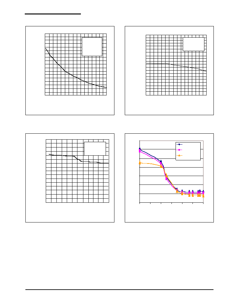
Output Noise vs. Bypass Capacitor Value
2.30
2.20
2.10
2.00
1.90
1.80
1.70
1.60
1.50
1.40
-40
-20
0
20
40
60
80
100 120
Temperature (∞C)
I
GND
(mA)
V
OUT
= 3.3V
V
IN
= 4.3V
C
L
= 1.0µF
I
L
= 150mA
1.60
1.50
1.40
1.30
1.20
1.10
1.00
0.90
0.80
4
6
8
10
12
14
16
V
IN
(V)
V
EN,
On Threshold
(V)
V
OUT
=3.3V
C
L
= 1.0µA
I
L
= 100µA
3.400
3.380
3.360
3.340
3.320
3.300
2.280
2.260
2.240
2.220
2.200
-40
-20
0
20
40
60
80 100 120
Temperature (∞C)
V
OUT
(V)
V
OUT
= 3.3V
V
IN
= 4.3V
C
L
= 1.0µF
TYPICAL PERFORMANCE CHARACTERISTICS: Continued
0
50
100
150
200
250
300
350
1
10
100
1000
10000
100000 1000000
Bypass Cap (pF)
uV RMS
Cin = 1uFT,
Cout = 1uFT
Cin = 1uFT,
Cout = 2.2uFT
Cin = 1uFT
Cout = 10uFT