 | –≠–ª–µ–∫—Ç—Ä–æ–Ω–Ω—ã–π –∫–æ–º–ø–æ–Ω–µ–Ω—Ç: SGL-0363 | –°–∫–∞—á–∞—Ç—å:  PDF PDF  ZIP ZIP |
Preliminary
Broomfield, CO 80021
1
EDS-104341 Rev D
The information provided herein is believed to be reliable at press time. Sirenza Microdevices assumes no responsibility for inaccuracies or omissions. Sirenza Microdevices assumes no responsibility for the use of this
information, and all such information shall be entirely at the user's own risk. Prices and specifications are subject to change without notice. No patent rights or licenses to any of the circuits described herein are implied or
granted to any third party. Sirenza Microdevices does not authorize or warrant any Sirenza Microdevices product for use in life-support devices and/or systems. Copyright 2001 Sirenza Microdevices, Inc.. All worldwide rights
reserved.
303 S. Technology Ct.
Phone: (800) SMI-MMIC http://www.sirenza.com
SGL-0363Z
5-2000 MHz Low Noise Amplifier
Silicon Germanium
Product Features
∑
Lead Free, RoHS Compliant & Green Package
∑
Low Power Consumption, 5.7mA @ 3.3V
∑
External Input Noise Match
∑
High Gain and Low Noise,
20dB and 1.1dB respectively @ 900MHz
∑
Operates from 2.7 to 3.3V
∑
Power Shutdown Capability using V
PC
∑
500V ESD, Class 1B
∑
Small Package: SOT-363
∑
High input overdrive capability, +18dBm
Applications
∑
Low Power LNA for ISM,
Cellular and Mobile Communications
Pb
RoHS Compliant
&
Package
Green
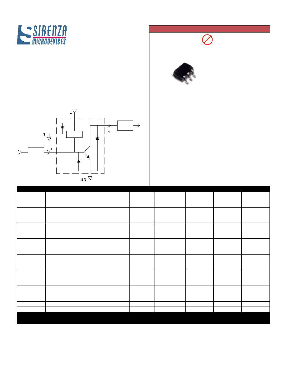
Product Description
Sirenza Microdevices' SGL-0363Z is a low power, low noise amplifier. It is
designed for 2.7 to 3.3V battery operation. The matching networks are
implemented externally which allows for optimum narrow-band performance
with 20dB typical gain and 1.1dB noise figure from 200-900MHz. This RFIC
uses the latest Silicon Germanium HBT process.
The matte tin finish on Sirenza's lead-free "Z" package is applied using a post
annealing process to mitigate tin whisker formation and is RoHS compliant per
EU Directive 2002/95. The package body is manufactured with green molding
compounds that contain no antimony trioxide or halogenated fire retardants.
RF Out
Simplified Device Schematic
Vpc
Gnd
RF In
Gnd
Active Bias
Network
Narrow-band
Matching
Network
Narrow-band
Matching
Network
Symbol
Parameters
Units
Frequency
Min.
Typ.
Max.
200 MHz
21
450 MHz
20
900 MHz
17
20
23
200 MHz
1.1
450 MHz
2.2
900 MHz
2.5
200 MHz
-3.8
450 MHz
-2.4
900 MHz
-7.1
200 MHz
1.0
450 MHz
1.1
900 MHz
1.1
200 MHz
14
450 MHz
12
900 MHz
15
200 MHz
20
450 MHz
19
900 MHz
12
200 MHz
24
450 MHz
25
900 MHz
27
I
D
Device Operating Current
mA
4.8
5.7
6.6
R
TH
, j-l
Thermal Resistance (junction - lead)
∞C/W
173
S
21
Small Signal Gain
dB
P
1dB
Output Power at 1dB Compression
dBm
IIP
3
Input Third Order Intercept Point
dBm
NF
Noise Figure
dBm
IRL
Input Return Loss
dBm
ORL
Output Return Loss
dBm
T
L
= 25∞C Z
S
= Z
L
= 50 Ohms Different Application Circuit per Band
S12
Reverse Isolation
dBm
Test Conditions: V
S
= 3.3V I
D
= 5.7mA Typ. IIP
3
Tone Spacing = 1MHz, Pout per tone = -15 dBm

Broomfield, CO 80021
2
EDS-104341 Rev D
Preliminary
303 S. Technology Ct.
Phone: (800) SMI-MMIC http://www.sirenza.com
SGL-0363Z 5-2000 MHz SiGe Low Noise Amplifier
Absolute Maximum Ratings
DCIV over Temperature
0
1
2
3
4
5
6
7
8
0
1
2
3
4
Vd (V)
Id
(
m
A
)
25C
-40C
85C
4 GHz
3 GHz
2 GHz
.9 GHz
.45 GHz
.2 GHz
S11 Vs.
Frequency
Insertion Gain & Isolation
0
5
10
15
20
25
30
0
0.5
1
1.5
2
2.5
3
3.5
4
Frequency (GHz)
G
a
in (
d
B
)
-35
-30
-25
-20
-15
-10
-5
Is
ola
t
ion (
d
B
)
Max Gain
Gain
Isolation
Note: S-parameters are de-embedded to the device leads with ZS=ZL=50
. The device was mounted on eval. board 125390-B and grounded like 900MHz
application circuit. De-embedded S-parameters can be downloaded from our website (www.sirenza.com)
2 GHz
3 GHz
4 GHz
.9 GHz
.45 GHz
.2 GHz
S22 Vs.
Frequency
Typical Performance - De-embedded S-parameters
Caution: ESD Sensitive
Appropriate precautions in handling, packaging
and testing devices must be observed.
Parameter
Absolute Limit
Max Device Current (I
D
)
20mA
Max Device Voltage (V
D
)
5.5 V
Max. RF Input Power* (See Note)
+18 dBm
Max. Junction Temp. (T
J
)
+150∞C
Operating Temp. Range (T
L
)
-40∞C to +85∞C
Max. Storage Temp.
+150∞C
I
D
V
D
< (T
J
- T
L
) / R
TH
, j-l T
L
=T
LEAD
Bias Conditions should also satisfy the following expression:
*Note: Load condition 1, Z
L
= 50 Ohms
Load condition 2, Z
L
= 10:1 VSWR
Operation of this device beyond any one of these limits may cause
permanent damage. For reliable continuous operation, the device
voltage and current must not exceed the maximum operating values
specified in the table on page one.
Parameter
Rating
ESD Rating - Human Body Model (HBM)
Class 1B
Moisture Sensitivity Level
MSL 1
Reliability & Qualification Information
This product qualification report can be downloaded at www.sirenza.com

Broomfield, CO 80021
3
EDS-104341 Rev D
Preliminary
303 S. Technology Ct.
Phone: (800) SMI-MMIC http://www.sirenza.com
SGL-0363Z 5-2000 MHz SiGe Low Noise Amplifier
200 MHz Application Circuit Data, V
S
= 3.3V, I
D
= 5.7mA
Note: Tuned for NF
Gain vs. Frequency
16
18
20
22
24
170
180
190
200
210
220
230
Frequency (MHz)
G
a
in (
d
B
)
S21_25C
S21_-40C
S21_85C
Input/Output Return Loss,
Isolation vs. Frequency, T=25C
-30
-25
-20
-15
-10
-5
0
170
180
190
200
210
220
230
Frequency (MHz)
dB
S11
S12
S22
P1dB vs. Frequency
-2
-1
0
1
2
3
4
5
6
170
180
190
200
210
220
230
Frequency (MHz)
P1
d
B
(
d
B
m
)
25C
-40C
85C
IM3 vs. Tone Power @200MHz
-80
-70
-60
-50
-40
-30
-19
-17
-15
-13
-11
-9
-7
-5
Pout per tone (dBm)
IM
3 (
d
B
c
)
25C
-40C
85C
OIP3 vs. Freq. (-15dBm Output Tones)
11
12
13
14
15
16
17
18
19
20
170
180
190
200
210
220
230
Frequency (MHz)
OI
P
3
(
d
B
m
)
25C
-40C
85C
Noise Figure vs. Frequency
0.4
0.6
0.8
1
1.2
1.4
1.6
1.8
2
170
180
190
200
210
220
230
Frequency (MHz)
NF
(
d
B)
85C
25C

Broomfield, CO 80021
4
EDS-104341 Rev D
Preliminary
303 S. Technology Ct.
Phone: (800) SMI-MMIC http://www.sirenza.com
SGL-0363Z 5-2000 MHz SiGe Low Noise Amplifier
450 MHz Application Circuit Data, V
S
= 3.3V, I
D
= 5.7mA
Note: Tuned for NF
Gain vs. Frequency
16
18
20
22
24
420
430
440
450
460
470
480
Frequency (MHz)
G
a
in
(
d
B
)
S21_25C
S21_-40C
S21_85C
Input/Output Return Loss,
Isolation vs. Frequency, T=25C
-30
-25
-20
-15
-10
-5
0
420
430
440
450
460
470
480
Frequency (MHz)
dB
S11
S12
S22
P1dB vs. Frequency
-2
-1
0
1
2
3
4
5
6
420
430
440
450
460
470
480
Frequency (MHz)
P1
d
B
(
d
Bm
)
25C
-40C
85C
IM3 vs. Tone Power @450MHz
-80
-70
-60
-50
-40
-30
-19
-17
-15
-13
-11
-9
-7
-5
Pout per tone (dBm)
IM
3 (
d
B
c
)
25C
-40C
85C
OIP3 vs. Freq. (-15dBm Output Tones)
11
12
13
14
15
16
17
18
19
20
420
430
440
450
460
470
480
Frequency (MHz)
OI
P
3
(
d
B
m
)
25C
-40C
85C
Noise Figure vs. Frequency
0.4
0.6
0.8
1
1.2
1.4
1.6
1.8
2
420
430
440
450
460
470
480
Frequency (MHz)
NF
(
d
B)
25C
85C

Broomfield, CO 80021
5
EDS-104341 Rev D
Preliminary
303 S. Technology Ct.
Phone: (800) SMI-MMIC http://www.sirenza.com
SGL-0363Z 5-2000 MHz SiGe Low Noise Amplifier
900 MHz Application Circuit Data, V
S
= 3.3V, I
D
= 5.7mA
Note: Tuned for NF
Gain vs. Frequency
16
18
20
22
24
870
880
890
900
910
920
930
Frequency (MHz)
G
a
in
(
d
B
)
S21_25C
S21_-40C
S21_85C
Input/Output Return Loss,
Isolation vs. Frequency, T=25C
-30
-25
-20
-15
-10
-5
0
870
880
890
900
910
920
930
Frequency (MHz)
dB
S11
S12
S22
P1dB vs. Frequency
-2
-1
0
1
2
3
4
5
6
870
880
890
900
910
920
930
Frequency (MHz)
P1
d
B
(
d
B
m
)
25C
-40C
85C
OIP3 vs. Freq. (-15dBm Output Tones)
11
12
13
14
15
16
17
18
19
20
870
880
890
900
910
920
930
Frequency (MHz)
OI
P
3
(d
B
m
)
25C
-40C
85C
IM3 vs. Tone Power @900MHz
-80
-70
-60
-50
-40
-30
-19
-17
-15
-13
-11
-9
-7
-5
Pout per tone (dBm)
IM
3
(
d
B
c
)
25C
-40C
85C
Noise Figure vs. Frequency
0.4
0.6
0.8
1
1.2
1.4
1.6
1.8
2
870
880
890
900
910
920
930
Frequency (MHz)
NF
(
d
B)
85C
25C