
The information provided herein is believed to be reliable at press time. Sirenza Microdevices assumes no responsibility for inaccuracies or ommisions.
Sirenza Microdevices assumes no responsibility for the use of this information, and all such information shall be entirely at the user's own risk. Prices and specifications are subject to change without
notice. No patent rights or licenses to any of the circuits described herein are implied or granted to any third party. Sirenza Microdevices does not authorize or warrant any Sirenza Microdevices product
for use in life-support devices and/or systems.
Copyright 2002 Sirenza Microdevices, Inc. All worldwide rights reserved.
303 South Technology Court, Broomfield, CO 80021
Phone: (800) SMI-MMIC
http://www.sirenza.com
1
EDS-102750 Rev D
Preliminary
Consumer products, such as Set-Top boxes, PVR's, Home
Gateways, and Cable Modems, often require a technique
for "splitting" the incoming RF CATV signal, to perform var-
ious functions, such as picture-in-picture, VOIP, data, and
video recording.
Sirenza Microdevices' CGA-0116 is a high performance 3-
output broadband CATV active splitter-amplifier, designed
for operation at 5V. It offers flat gain, high isolation, high
IP2, and low power consumption.
This RFIC uses the latest Silicon Germanium
Heterostructure Bipolar Transistor (SiGe HBT) process
featuring 2 micron emitters.
Key Specifications
Symbol
Parameters: Test Conditions
Z
0
= 75
, V
CC
= 5.0V, I = 150mA, T
BP
= 30�C
Unit
Min.
Typ.
Max.
f
0
Frequency of Operation
MHz
50
870
I
Current
135
150
165
P
1dB
Output Power at 1dB Compression - Channels 1&2 @ 500MHz
dB
�
V
114.5
116
Output Power at 1 dB Compression - Channel 3 @ 870MHz
dB
�
V
118.5
120
S
21
Small Signal Gain - Channels 1&2 @ 870MHz
dB
1.8
2.3
2.8
Small Signal Gain - Channel 3 @ 870MHz
dB
6.5
7.5
8.5
IRL
Input Return Loss 50MHz to 870MHz
dB
7.5
9
ORL
Output Return Loss 50MHz to 870MHz
dB
11
13
OIP
3
Output Third Order Intercept Point - Channels 1&2 @ 500MHz
dB
�
V
127
129
Output Third Order Intercept Point - Channel 3 @ 500MHz
dB
�
V
132
134
OIP
2
Output Second Order Intercept Point - Channels 1&2 @ 500MHz
dB
�
V
146
149
Output Second Order Intercept Point - Channel 3 @ 500MHz
dB
�
V
152
155
NF
Noise Figure - Channels 1&2 @ 870Mhz
dB
7.5
8.5
Noise Figure - Channel 3 @ 870MHz
dB
7.5
8.5
S
12
Isolation, Channel-to-Channel 50MHz to 870MHz
dB
32
35
Isolation, Output-to-Input 50MHz to 870MHz
dB
37
40
R
TH, j-l
Thermal Resistance (junction - lead)
�C/W
70
Functional Block Diagram
CGA-0116
3-Output Active Splitter for CATV
Product Features
Applications
�
Broad Frequency Band: 50 to 870 MHz
�
Flat Gain Response: <
6
0.5 dB Variance
�
Internally Matched to 75
�
High Isolation between Output Ports: >35 dB
�
High IP2: >149 dB
�
V
�
Single Voltage Supply
�
Patent Pending
�
Set-top Box
�
Cable Modem
�
PVR
Product Description
16 pin TSSOP Package with Exposed Ground Pad
Vctl 3
GND
Vin
Vb
IN
Rb
GND
Vctl 1
Ch3
GND
GND
Vctl 2
Ch2
GND
GND
Ch1
1
2
3
4
5
6
7
8
16
15
14
13
12
11
10
9

303 South Technology Court, Broomfield, CO 80021
Phone: (800) SMI-MMIC
http://www.sirenza.com
2
EDS-102750 Rev D
Preliminary
CGA-0116 3-Output CATV Active Splitter
Pin Out Description
Pin #
Function
Description
1
Vctl 3
Gain adjust for Output 3. This pin should be bypassed to ground for max gain
2,7,10
11,14,
15
GND
Connection to ground.
3
Vin
Voltage supply connection for input. This pin should be bypassed with a suitable capacitor.
4
Vb
Bias connection for input. This pin should be bypassed with a suitable capacitor
5
IN
RF input pin. This pin requires a DC blocking capacitor
6
Rb
Input bias resistor connection for setting bias current. This pin should be connected to groung for specified
operation.
8
Vctl 1
Gain adjust for Output 3. This pin should be bypassed to ground for max gain
9
Ch. 1
RF Output 1 and DC supply pin. This pin required the use of an external blocking capacitor and RF choke.
12
Ch. 2
RF Output 2 and DC supply pin. This pin required the use of an external blocking capacitor and RF choke.
13
Vctl 2
Gain adjust for Output 3. This pin should be bypassed to ground for max gain
16
Ch. 3
RF Output 3 and DC supply pin. This pin required the use of an external blocking capacitor and RF choke.
Back-
side
GND
The exposed backside paddle needs to be well grounded with multiple vias. This is the main electrical GND
and the main thermal path.
Caution: ESD Sensitive
Appropriate precaution in handling, packaging
and testing devices must be observed.
Simplified Device Schematic
Absolute Maximum Ratings
Parameters
Value
Unit
Current
200
mA
Device Voltage (V
D
)
6.0
V
Power Dissipation
1.2
W
Operating Lead Temperature (T
L
)
-40 to +85
�C
RF Input Power
15
dBm
Storage Temperature Range
-40 to +150
�C
Operating Junction Temperature (T
J
)
+150
�C
Operation of this device beyond any one of these limits may
cause permanent damage. For reliable continuous operation
the device voltage and current must not exceed the maximum
operating values specified in the table on page one.
Bias conditions should also satisfy the following expression:
I
D
V
D
< (T
J
- T
L
) / R
TH'
j-l
RFout
RFout
RFout
RFin
303 South Technology Court, Broomfield, CO 80021
Phone: (800) SMI-MMIC
http://www.sirenza.com
3
EDS-102750 Rev D
Preliminary
CGA-0116 3-Output CATV Active Splitter
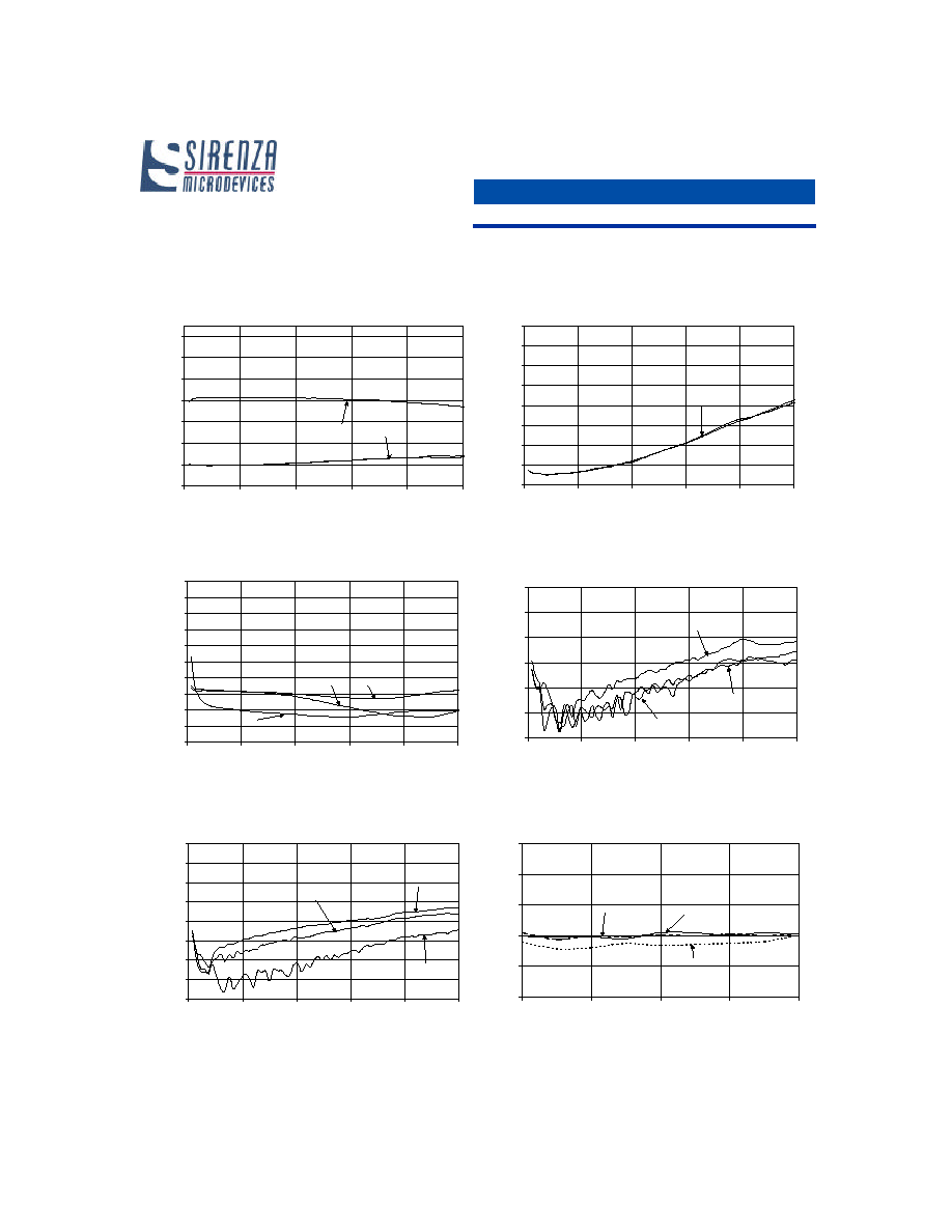
Evaluation Board Data (V
CC
= 5.0V, I
CC
= 150mA)
Gain vs Frequency
0
2
4
6
8
10
12
14
0
200
400
600
800
1000
Frequency (MHz)
Gain (dB)
Ch 1 & Ch 2
Ch 3
Input Return Loss Vs. Freq
-16
-14
-12
-10
-8
-6
-4
-2
0
0
200
400
600
800
1000
Frequency (MHz)
s11 (dB)
Ch 1
Output Return Loss vs Frequency
-20
-18
-16
-14
-12
-10
-8
-6
-4
-2
0
0
200
400
600
800
1000
Frequency(MHz)
S22 (dB)
Ch 2
Ch 1
Ch 3
Isolation Channel Output to RF Input
-80
-70
-60
-50
-40
-30
-20
0
200
400
600
800
1000
Frequency (MHz)
dB
Ch 2 to Input
Ch 3 to Input
Ch 1 to Input
Isolation vs Frequency
-80
-70
-60
-50
-40
-30
-20
-10
0
0
200
400
600
800
1000
Frequency(MHz)
dB
Ch 3 to Ch 2
Ch 2 to Ch 1
Ch 3 to Ch 1
Noise Figure vs Frequency
5
6
7
8
9
10
100
300
500
700
900
Frequency (MHz)
NF (dB)
Ch 1
Ch 2
Ch 3

303 South Technology Court, Broomfield, CO 80021
Phone: (800) SMI-MMIC
http://www.sirenza.com
4
EDS-102750 Rev D
Preliminary
CGA-0116 3-Output CATV Active Splitter
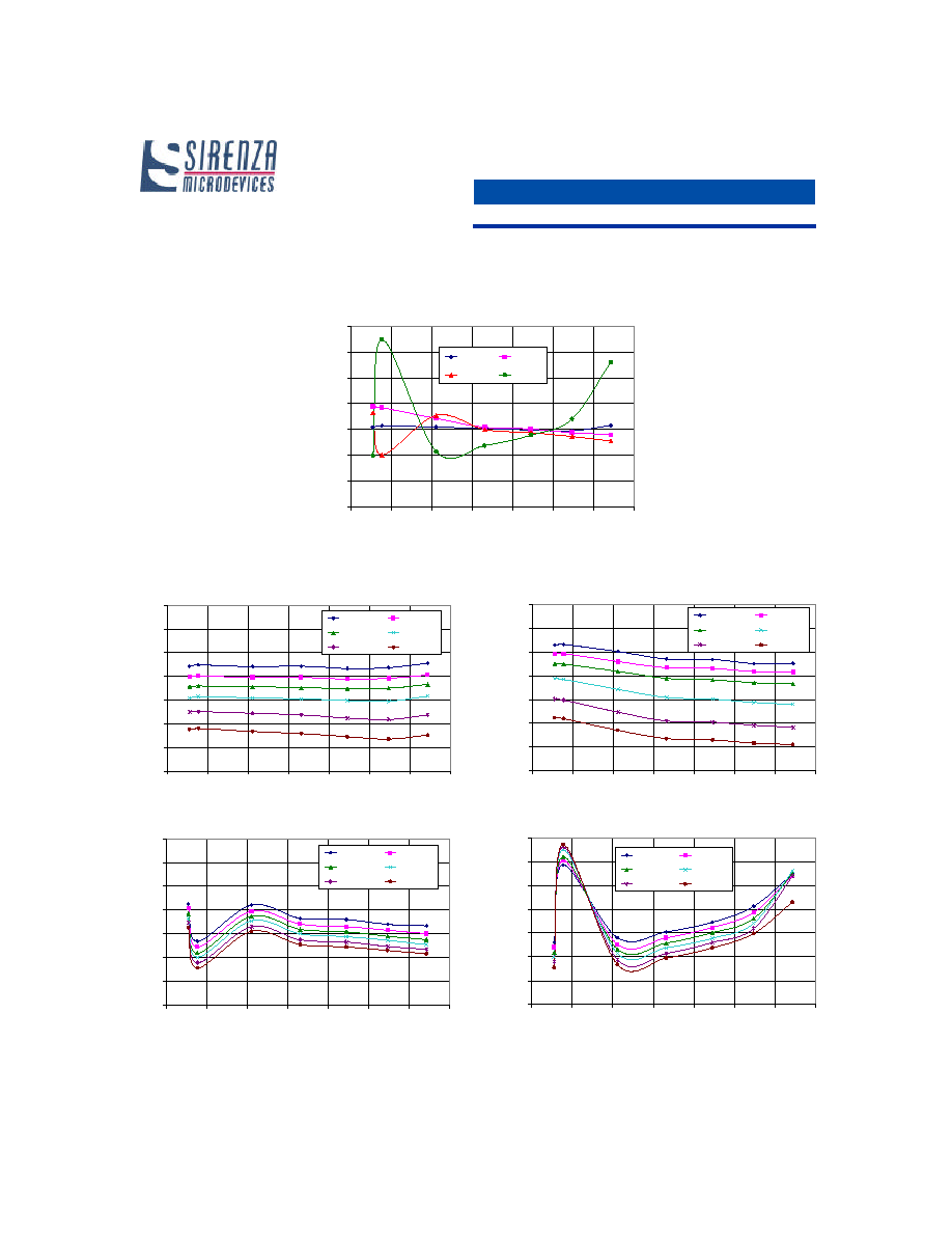
Channel 1 Gain vs Temperature
0
1
2
3
4
5
6
0
200
400
600
800
1000
Frequency(MHz)
dB
- 40c
+ 85c
+ 25c
Channel 2 Gain vs Temperature
0
1
2
3
4
5
6
0
200
400
600
800
1000
Frequency (MHz)
Gain(dB)
- 40c
+ 25c
+ 85c
Ch 3 Gain vs Temperature
5
6
7
8
9
10
0
200
400
600
800
1000
Frequency(MHz)
Gain(dB)
- 40c
+ 25c
+85c
P1dB vs. Temperature (500 MHz)
100
105
110
115
120
125
130
-40
-15
10
35
60
85
Temperature (C)
P1dB (dB
�
V)
Channel
3
Channel 1 & 2
IP3 vs. Temperature (500 MHz)
120
125
130
135
140
145
150
-40
-15
10
35
60
85
Temperature (C)
IP3 (dB
�
V)
Ch 1 & 2
Ch3
Evaluation Board Data (V
CC
= 5.0V, I
CC
= 150mA)
IP2 vs. Temperature (500 MHz)
130
135
140
145
150
155
160
165
170
-40
-15
10
35
60
85
Temperature (C)
IP2 (dB
�
V)
Ch1 & Ch2
Ch3

303 South Technology Court, Broomfield, CO 80021
Phone: (800) SMI-MMIC
http://www.sirenza.com
5
EDS-102750 Rev D
Preliminary
CGA-0116 3-Output CATV Active Splitter
30
40
50
60
70
80
90
100
0
100
200
300
400
500
600
700
Frequency (MHz)
dBc
XMOD
CTB
CSO+
CSO-
Evaluation Board Data (V
CC
= 5.0V, I
CC
= 150mA)
Channel 1 and 2 Composite Performance:
Ch. 1 Measured Data Shown
Channel 1 & 2 Composite Performance vs. Input Power Level, 100 Ch., Flat:
CTB/CSO/XMOD, Ch. 1 & 2
Input Power 76 dBuV/Ch., 100 Ch., Flat
CGA-0116 Ch. 1 & 2: XMOD vs. Pin and Freq.
30
40
50
60
70
80
90
100
0
100
200
300
400
500
600
700
Frequency (MHz)
dBc
74dBuV
76dBuV
78dBuV
80dBuV
82dBuV
84dBuV
CGA-0116 Ch. 1 & 2: CTB vs. Pin and Freq.
30
40
50
60
70
80
90
100
0
100
200
300
400
500
600
700
Frequency (MHz)
dBc
74dBuV
76dBuV
78dBuV
80dBuV
82dBuV
84dBuV
CGA-0116 Ch. 1 & 2: CSO+ vs. Pin and Freq.
30
40
50
60
70
80
90
100
0
100
200
300
400
500
600
700
Frequency (MHz)
dBc
74dBuV
76dBuV
78dBuV
80dBuV
82dBuV
84dBuV
CGA-0116 Ch. 1 & 2: CSO- vs. Pin and Freq.
30
40
50
60
70
80
90
100
0
100
200
300
400
500
600
700
Frequency (MHz)
dBc
74dBuV
76dBuV
78dBuV
80dBuV
82dBuV
84dBuV
303 South Technology Court, Broomfield, CO 80021
Phone: (800) SMI-MMIC
http://www.sirenza.com
6
EDS-102750 Rev D
Preliminary
CGA-0116 3-Output CATV Active Splitter
30
40
50
60
70
80
90
100
0
100
200
300
400
500
600
700
Frequency (MHz)
dBc
XMOD
CTB
CSO+
CSO-
Channel 3 Composite Performance:
Evaluation Board Data (V
CC
= 5.0V, I
CC
= 150mA)
CTB/CSO/XMOD, Ch. 3
Input Power 76 dBuV/Ch., 100 Ch., Flat
CGA-0116 Ch. 3: XMOD vs. Pin and Freq.
30
40
50
60
70
80
90
100
0
100
200
300
400
500
600
700
Frequency (MHz)
dBc
74dBuV
76dBuV
78dBuV
80dBuV
82dBuV
84dBuV
CGA-0116 Ch. 3: CTB vs. Pin and Freq.
30
40
50
60
70
80
90
100
0
100
200
300
400
500
600
700
Frequency (MHz)
dBc
74dBuV
76dBuV
78dBuV
80dBuV
82dBuV
84dBuV
CGA-0116 Ch. 3: CSO- vs. Pin and Freq.
30
40
50
60
70
80
90
100
0
100
200
300
400
500
600
700
Frequency (MHz)
dBc
74dBuV
76dBuV
78dBuV
80dBuV
82dBuV
84dBuV
Channel 3 Composite Performance vs. Input Power Level, 100 Ch., Flat:
CGA-0116 Ch. 3: CSO+ vs. Pin and Freq.
30
40
50
60
70
80
90
100
0
100
200
300
400
500
600
700
Frequency (MHz)
dBc
74dBuV
76dBuV
78dBuV
80dBuV
82dBuV
84dBuV
303 South Technology Court, Broomfield, CO 80021
Phone: (800) SMI-MMIC
http://www.sirenza.com
7
EDS-102750 Rev D
Preliminary
CGA-0116 3-Output CATV Active Splitter
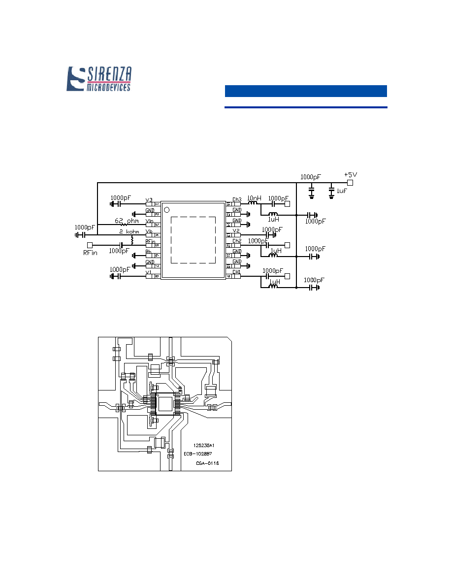
Evaluation Board Schematic
Evaluation Board Layout
C14
C7
C6
R3
C2
C1
R2
R1
NOTE: VIAS NOT SHOWN
R3 2K ohm
R2 62 ohm
R1 0 ohm
L1,L2,L3 1uH
C2,C6,C7,C8,C9,C10,C11,
C12,C13,C14,C15,C16 1000pF
C1 0.1uF
Component Value
L2
C13
C12
L1
C16
C15
C10
C11
C8
L3
C9
L4
L4 10nH 0402 size
303 South Technology Court, Broomfield, CO 80021
Phone: (800) SMI-MMIC
http://www.sirenza.com
8
EDS-102750 Rev D
Preliminary
CGA-0116 3-Output CATV Active Splitter
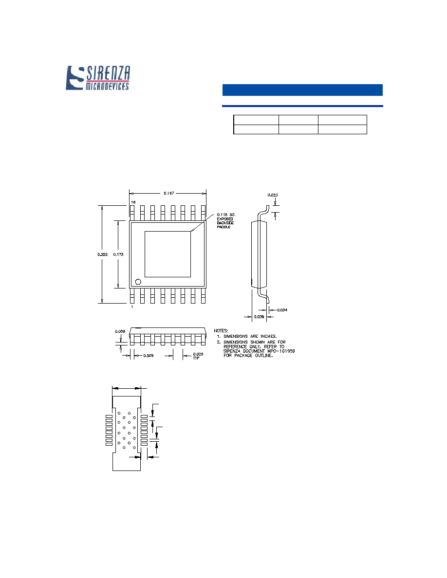
Package Outline Drawing
CGA
0116
LOT ID
Part Number Ordering Information
Part Number
Reel Size
Devices/Reel
CGA-0116
7"
1000
Part Symbolization
The part will be symbolized with an "CGA-0116"
marking designator on the top surface of the pack-
0.026
0.017
0.043
0.198
Recommended Land Pattern
Note 1: Dimensions are in inches