The information provided herein is believed to be reliable at press time. Sirenza Microdevices assumes no responsibility for inaccuracies or ommisions.
Sirenza Microdevices assumes no responsibility for the use of this information, and all such information shall be entirely at the user's own risk. Prices and specifications are subject to change without
notice. No patent rights or licenses to any of the circuits described herein are implied or granted to any third party. Sirenza Microdevices does not authorize or warrant any Sirenza Microdevices product
for use in life-support devices and/or systems.
Copyright 2002 Sirenza Microdevices, Inc. All worldwide rights reserved.
303 South Technology Court Broomfield, CO 80021
Phone: (800) SMI-MMIC
http://www.sirenza.com
1
EDS-104611 Rev C
Preliminary
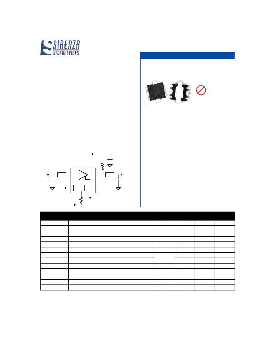
Sirenza Microdevices' SZP-2026Z is a high linearity single
stage class AB Heterojunction Bipolar Transistor (HBT)
amplifier housed in a proprietary surface-mountable plastic
encapsulated package. This HBT amplifier is made with
InGaP on GaAs device technology and fabricated with
MOCVD for an ideal combination of low cost and high reli-
ability.
This product is specifically designed as a flexible final or
driver stage for 802.16 and 802.11 equipment in the 2.2-
2.7GHz bands. It can run from a 3V to 6V supply. It is pre-
matched to ~5 ohms on the input for broadband perfor-
mance and ease of matching at the board level. It features
an output power detector, on/off power control, ESD protec-
tion, excellent overall robustness and a proprietary hand
reworkable and thermally enhanced SOF-26 package. This
product features a RoHS Compliant and Green package
with matte tin finish, designated by the `Z' suffix.
Key Specifications
Symbol
Parameters: Test Conditions, 2.5-2.7GHz App circuit,
Z
0
= 50
, V
CC
= 5.0V, Iq = 445mA, T
BP
= 30�C
Unit
Min.
Typ.
Max.
f
O
Frequency of Operation
MHz
2200
2700
P
1dB
Output Power at 1dB Compression � 2.7GHz
dBm
31.5
33
S
21
Small Signal Gain � 2.7GHz
dB
11.3
12.8
Pout
Output power at 2.5% EVM 802.11g 54Mb/s - 2.5GHz
dBm
26.2
IM3
Third Order Suppression (Pout=23dBm per tone) - 2.7GHz
dBc
-45
-42
NF
Noise Figure at 2.7GHz
dB
4.3
IRL
Worst Case Input Return Loss 2.5-2.7GHz
dB
8
12
ORL
Worst Case Output Return Loss 2.5-2.7GHz
8
12
Vdet Range
Output Voltage Range for Pout=10dBm to 33dBm
V
0.85 to 1.4
I
cq
Quiescent Current (V
cc
= 5V)
mA
395
445
495
I
VPC
Power Up Control Current (V
pc
= 5V)
mA
2.1
I
leak
Vcc Leakage Current (V
cc
= 5V, V
pc
= 0V)
�
A
10
R
th, j-l
Thermal Resistance (junction - lead)
�C/W
12
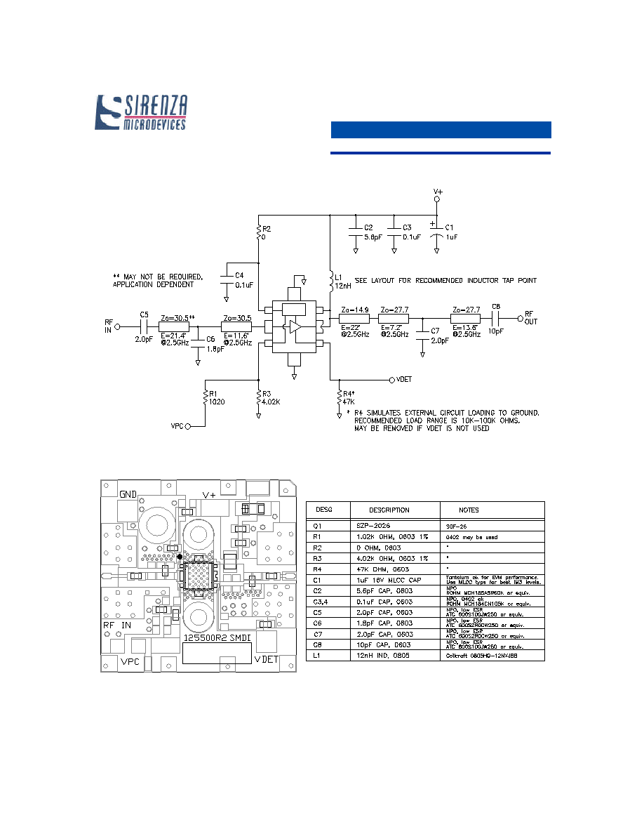
Functional Block Diagram
SZP-2026Z
2.2-2.7GHz 2W InGaP Amplifier
Product Features
Applications
�
P1dB = 33.5dBm @ 5V, 2.4GHz
�
802.11g 54Mb/s Class AB Performance
Pout = 26dBm @ 2.5%EVM, Vcc 5V
Pout = 27dBm @ 2.5% EVM, Vcc 6V
�
On-chip Output Power Detector
�
Input Prematched to ~5 ohms
�
Proprietary Low Thermal Resistance Package
Hand Solderable and Easy Rework
�
Power up/down control < 1
�
s
�
802.16 WiMAX Driver or Output Stage
�
2.4GHz 802.11 WLAN and ISM Applications
Product Description
Proprietary SOF-26 Package
Active
Bias
RFIN
RFOUT
Power
Detector
Vbias = 5V
Power
Up/Dow n
Control
Vcc = 5V
SZP-2026
Pb
RoHS Compliant
& Package
Green
303 South Technology Court Broomfield, CO 80021
Phone: (800) SMI-MMIC
http://www.sirenza.com
2
EDS-104611 Rev C
Preliminary
SZP-2026Z 2.2-2.7GHz 2W Power Amp
Typical Performance 2.4-2.5GHz App Circuit (Vcc=5V, Icq=445mA, * 802.11g 54Mb/s 64QAM)
Parameter
Units
2.4GHz
2.5GHz
Gain
dB
13.3
13.0
P1dB
dBm
33.5
33.3
Pout @ 2.5% EVM*
dBm
26
26
Current @ Pout 2.5% EVM*
mA
550
545
Input Return Loss
dB
16
12
Output Return Loss
dB
16
16
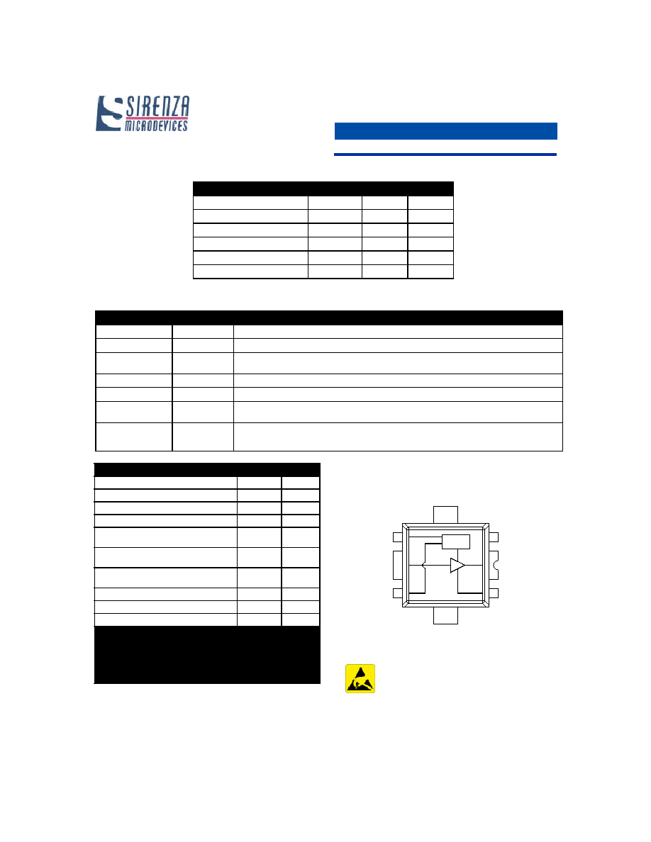
Caution: ESD Sensitive
Appropriate precaution in handling, packaging
and testing devices must be observed.
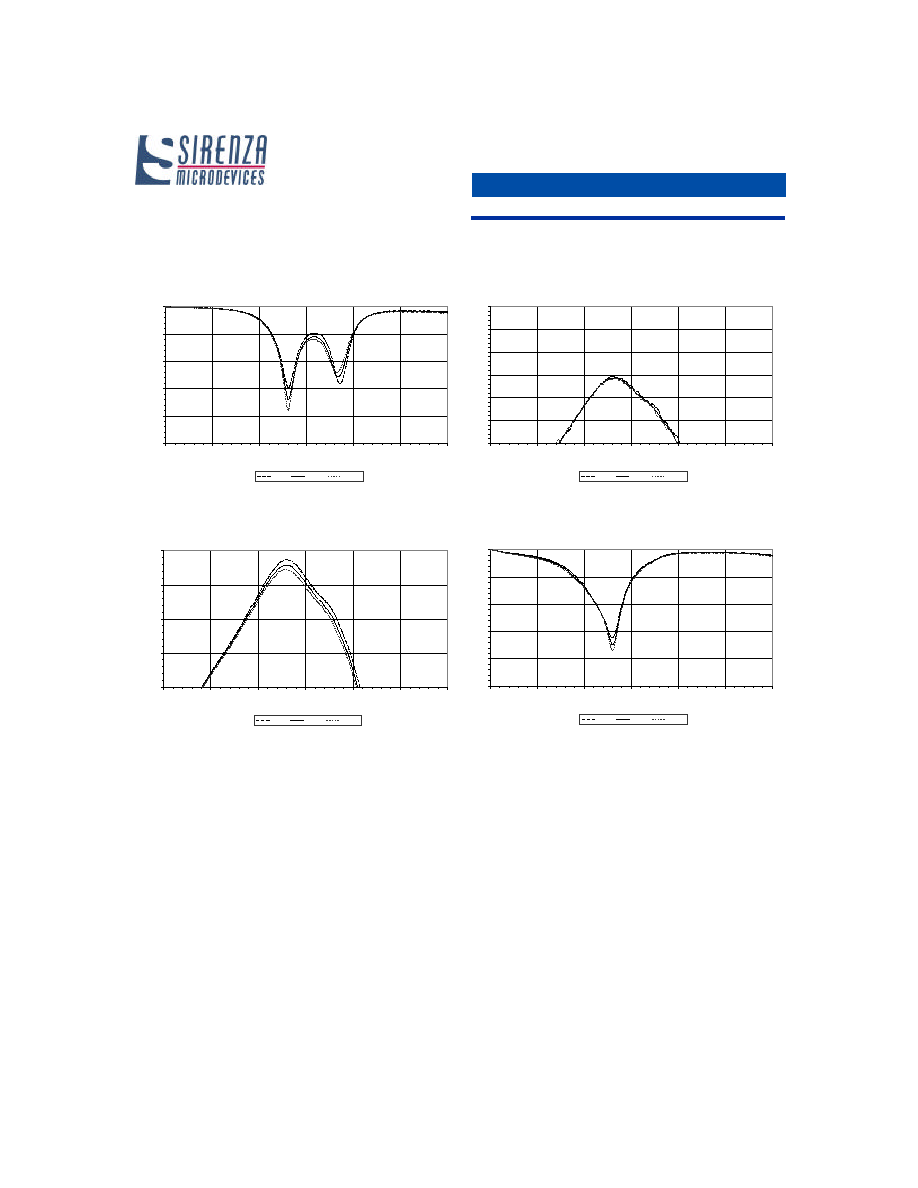
Typical Performance 2.5-2.7GHz - Refer to page 1 table
1
2
3
6
5
4
VBIAS
RFIN
VPC
VDET
RFOUT/VCC
NC
Bias
GND
GND
Absolute Maximum Ratings
Parameters
Value
Unit
VC1 Collector Bias Current (I
VC1
)
1500
mA
**Device Voltage (V
cc
)
7.0
V
Power Dissipation
6
W
Operating Lead Temperature (T
L
)
-40 to +85
�C
*Max RF output Power for 50 ohm contin-
uous long term operation
30
dBm
Max RF Input Power for 50 ohm output
load
28
dBm
Max RF Input Power for 10:1 VSWR out-
put load
23
dBm
Storage Temperature Range
-40 to +150
�C
Operating Junction Temperature (T
J
)
+150
�C
ESD Human Body Model
1000
V
Operation of this device beyond any one of these limits may
cause permanent damage. For reliable continuous operation
the device voltage and current must not exceed the maximum
operating values specified in the table on page one.
Bias conditions should also satisfy the following expression:
I
D
V
D
< (T
J
- T
L
) / R
TH'
j-l
Simplified Device Schematic
Pin Out Description
Pin #
Function
Description
1
VBIAS
This is the supply voltage for the active bias circuit.
2
RFIN
This is the RF input pin and has a DC voltage present. An external DC block is required.
3
VPC
Power up/down control pin. The voltage on this pin should never exceed the voltage on pin 3 by
more than 0.5V unless the supply current from pin 3 is limited < 10mA.
4
VDET
This is the output port for the power detector. It samples the power at the input of the amplifier.
5
RFOUT/VCC
This is the RF output pin and DC connection to the collector.
6
NC
This pin is not connected internal to the package. Buss it to pin 5 as shown on the app circuit to
achieve the specified performance.
GND
GND
These pins are DC connected to the backside paddle. They provide good thermal connection to the
backside paddle for hand soldering and rework. Many thermal and electrical GND vias are recom-
mended as shown in the landing pattern.
* With specified application circuit.
** No RF Drive
303 South Technology Court Broomfield, CO 80021
Phone: (800) SMI-MMIC
http://www.sirenza.com
3
EDS-104611 Rev C
Preliminary
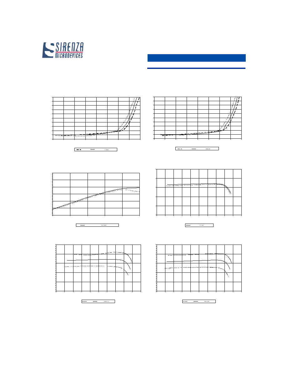
SZP-2026Z 2.2-2.7GHz 2W Power Amp
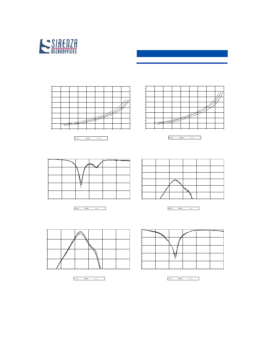
Measured 2.4-2.5 GHz Application Circuit Data (V
cc
= V
pc
= 5.0V, I
q
= 445mA, T=25C)
Source EVM = 0.6%, not deembedded from data.
IM3 vs Pout (2 Tone Avg.),T=+25c
Tone Spacing = 1MHz
-65
-60
-55
-50
-45
-40
-35
18
20
22
24
26
28
Pout(dBm)
IM3(dBc)
2.4GHz
2.5GHz
Typical Gain vs Pout, T=+25C
10
11
12
13
14
15
16
18
20
22
24
26
28
30
32
34
36
Pout(dBm)
Gain(dB)
2.4GHz
2.5GHz
Typical Gain vs Pout, F=2.4GHz
10
11
12
13
14
15
16
18
20
22
24
26
28
30
32
34
36
Pout(dBm)
Gain(dB)
-40c
+25c
+85c
Typical Gain vs Pout, F=2.5GHz
10
11
12
13
14
15
16
18
20
22
24
26
28
30
32
34
36
Pout(dBm)
Gain(dB)
-40c
+25c
+85c
EVM vs Pout F=2.4GHz
802.11g, OFDM 54Mb/S, 64QAM
0.0
0.5
1.0
1.5
2.0
2.5
3.0
3.5
4.0
4.5
5.0
12
14
16
18
20
22
24
26
28
Pout(dBm)
EVM(%)
-40c
+25c
+85c
EVM vs Pout F=2.5GHz
802.11g, OFDM 54Mb/S, 64QAM
0.0
0.5
1.0
1.5
2.0
2.5
3.0
3.5
4.0
4.5
5.0
12
14
16
18
20
22
24
26
28
Pout(dBm)
EVM(%)
-40c
+25c
+85c
303 South Technology Court Broomfield, CO 80021
Phone: (800) SMI-MMIC
http://www.sirenza.com
4
EDS-104611 Rev C
Preliminary
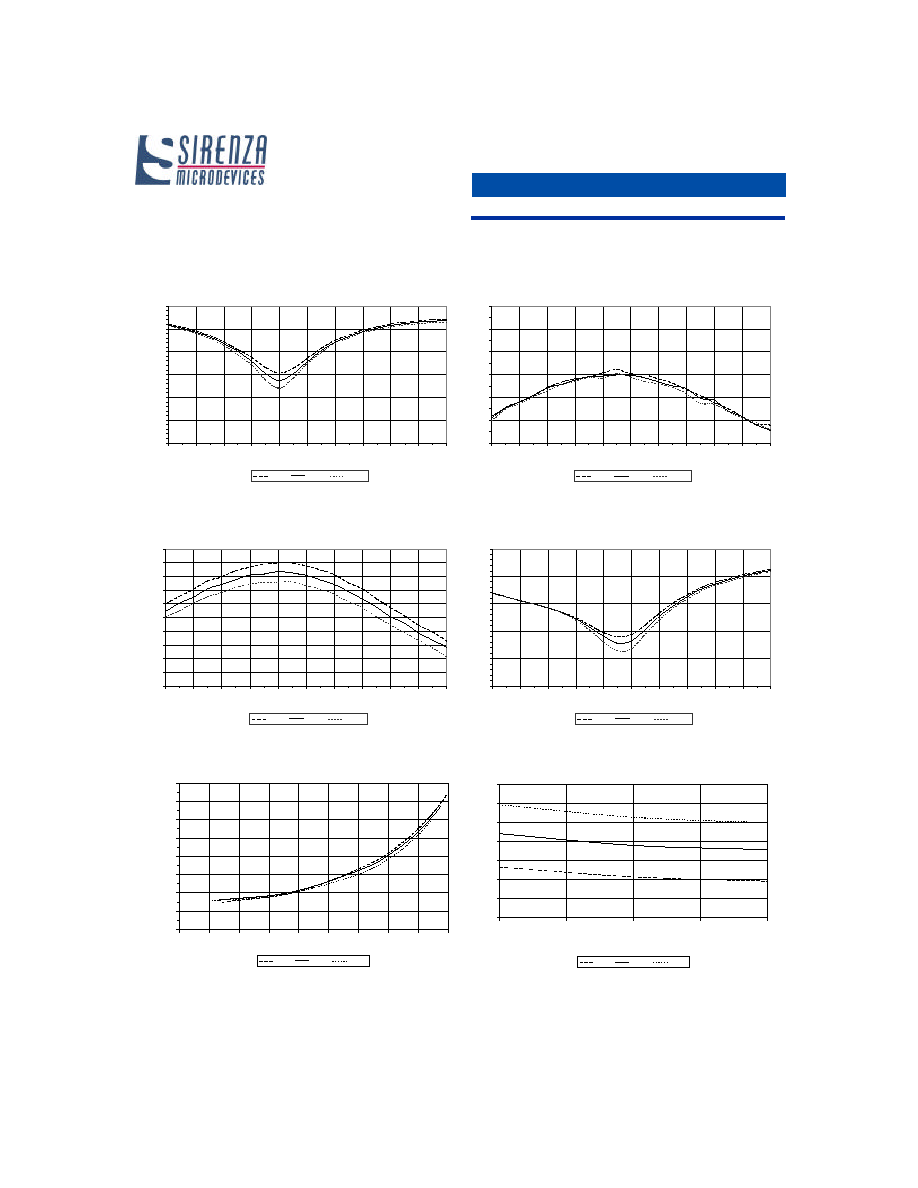
SZP-2026Z 2.2-2.7GHz 2W Power Amp
Measured 2.4-2.5 GHz Application Circuit Data (V
cc
= V
pc
= 5.0V, I
q
= 445mA, T=25C)
Narrowband S11 - Input Return Loss
-30
-25
-20
-15
-10
-5
0
2.0
2.1
2.2
2.3
2.4
2.5
2.6
2.7
2.8
2.9
3.0
Frequency(GHz)
S11(dB)
-40C
+25C
+85C
Narrowband S12 - Reverse Isolation
-32
-30
-28
-26
-24
-22
-20
2.0
2.1
2.2
2.3
2.4
2.5
2.6
2.7
2.8
2.9
3.0
Frequency(GHz)
S12(dB)
-40C
+25C
+85C
Narrowband S21 - Forward Gain
5
6
7
8
9
10
11
12
13
14
15
2.0
2.1
2.2
2.3
2.4
2.5
2.6
2.7
2.8
2.9
3.0
Frequency(GHz)
S21(dB)
-40C
+25C
+85C
Narrowband S22 - Output Return Loss
-25
-20
-15
-10
-5
0
2.0
2.1
2.2
2.3
2.4
2.5
2.6
2.7
2.8
2.9
3.0
Frequency(GHz)
S22(dB)
-40C
+25C
+85C
DC Supply Current vs Pout, F=2.4GHz
0.3
0.4
0.5
0.6
0.7
0.8
0.9
1
1.1
16
18
20
22
24
26
28
30
32
34
Pout(dBm)
Idc(A)
-40c
+25c
+85c
Noise Figure vs Frequency, O.T.
2.5
3
3.5
4
4.5
5
5.5
6
2.3
2.35
2.4
2.45
2.5
Frequency(GHz)
NF(dB)
-40c
+25c
+85c
303 South Technology Court Broomfield, CO 80021
Phone: (800) SMI-MMIC
http://www.sirenza.com
5
EDS-104611 Rev C
Preliminary
SZP-2026Z 2.2-2.7GHz 2W Power Amp
Measured 2.4-2.5 GHz Application Circuit Data (V
cc
= V
pc
= 5.0V, I
q
= 445mA, T=25C)
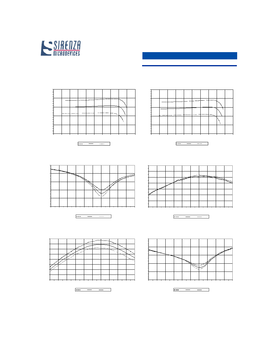
RF Power Detector (Vdet) vs Pout, F=2.4GHz
0.8
0.9
1
1.1
1.2
1.3
1.4
1.5
1.6
16
18
20
22
24
26
28
30
32
34
Pout(dBm)
Vdet(V)
-40c
+25c
+85c
RF Power Detector (Vdet) vs Pout, F=2.5GHz
0.8
0.9
1
1.1
1.2
1.3
1.4
1.5
1.6
16
18
20
22
24
26
28
30
32
34
Pout(dBm)
Vdet(V)
-40c
+25c
+85c
Broadband S11 - Input Return Loss
-25
-20
-15
-10
-5
0
0.0
1.0
2.0
3.0
4.0
5.0
6.0
Frequency(GHz)
S11(dB)
-40C
+25C
+85C
Broadband S12 - Reverse Isolation
-40
-35
-30
-25
-20
-15
-10
0.0
1.0
2.0
3.0
4.0
5.0
6.0
Frequency(GHz)
S12(dB)
-40C
+25C
+85C
Broadband S21 - Forward Gain
-5
0
5
10
15
0.0
1.0
2.0
3.0
4.0
5.0
6.0
Frequency(GHz)
S21(dB)
-40C
+25C
+85C
Broadband S22 - Output Return Loss
-25
-20
-15
-10
-5
0
0.0
1.0
2.0
3.0
4.0
5.0
6.0
Frequency(GHz)
S22(dB)
-40C
+25C
+85C
303 South Technology Court Broomfield, CO 80021
Phone: (800) SMI-MMIC
http://www.sirenza.com
6
EDS-104611 Rev C
Preliminary
SZP-2026Z 2.2-2.7GHz 2W Power Amp
Measured 2.5-2.7 GHz Application Circuit Data (V
cc
= V
pc
= 5.0V, I
q
= 445mA, T=25C)
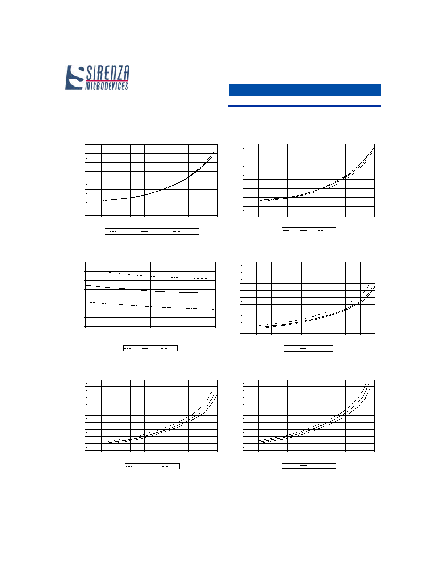
IM3 vs Pout (2 Tone Avg.),T=+25c
Tone Spacing = 1MHz
-65
-60
-55
-50
-45
-40
-35
18
20
22
24
26
28
Pout(dBm)
IM3(dBc)
2.5GHz
2.6GHz
2.7GHz
Typical Gain vs Pout, T=+25C
10
11
12
13
14
15
16
18
20
22
24
26
28
30
32
34
36
Pout(dBm)
Gain(dB)
2.5GHz
2.6GHz
2.7GHz
Typical Gain vs Pout, F=2.5GHz
10
11
12
13
14
15
16
18
20
22
24
26
28
30
32
34
36
Pout(dBm)
Gain(dB)
-40c
+25c
+85c
Source EVM = 0.6%, not deembedded from data.
EVM vs Pout F=2.5GHz
802.11g, OFDM 54Mb/S, 64QAM
0.0
0.5
1.0
1.5
2.0
2.5
3.0
3.5
4.0
4.5
5.0
12
14
16
18
20
22
24
26
28
Pout(dBm)
EVM(%)
-40c
+25c
+85c
EVM vs Pout F=2.6GHz
802.11g, OFDM 54Mb/S, 64QAM
0.0
0.5
1.0
1.5
2.0
2.5
3.0
3.5
4.0
4.5
5.0
12
14
16
18
20
22
24
26
28
Pout(dBm)
EVM(%)
-40c
+25c
+85c
EVM vs Pout F=2.7GHz
802.11g, OFDM 54Mb/S, 64QAM
0.0
0.5
1.0
1.5
2.0
2.5
3.0
3.5
4.0
4.5
5.0
12
14
16
18
20
22
24
26
28
Pout(dBm)
EVM(%)
-40c
+25c
+85c
303 South Technology Court Broomfield, CO 80021
Phone: (800) SMI-MMIC
http://www.sirenza.com
7
EDS-104611 Rev C
Preliminary
SZP-2026Z 2.2-2.7GHz 2W Power Amp
Measured 2.5-2.7 GHz Application Circuit Data (V
cc
= V
pc
= 5.0V, I
q
= 445mA, T=25C)
Typical Gain vs Pout, F=2.6GHz
10
11
12
13
14
15
16
18
20
22
24
26
28
30
32
34
36
Pout(dBm)
Gain(dB)
-40c
+25c
+85c
Typical Gain vs Pout, F=2.7GHz
10
11
12
13
14
15
16
18
20
22
24
26
28
30
32
34
36
Pout(dBm)
Gain(dB)
-40c
+25c
+85c
Narrowband S11 - Input Return Loss
-25
-20
-15
-10
-5
0
2.0
2.1
2.2
2.3
2.4
2.5
2.6
2.7
2.8
2.9
3.0
Frequency(GHz)
S11(dB)
-40C
+25C
+85C
Narrowband S12 - Reverse Isolation
-36
-34
-32
-30
-28
-26
-24
-22
2.0
2.1
2.2
2.3
2.4
2.5
2.6
2.7
2.8
2.9
3.0
Frequency(GHz)
S12(dB)
-40C
+25C
+85C
Narrowband S21 - Forward Gain
6
7
8
9
10
11
12
13
14
2.0
2.1
2.2
2.3
2.4
2.5
2.6
2.7
2.8
2.9
3.0
Frequency(GHz)
S21(dB)
-40C
+25C
+85C
Narrowband S22 - Output Return Loss
-25
-20
-15
-10
-5
0
2.0
2.1
2.2
2.3
2.4
2.5
2.6
2.7
2.8
2.9
3.0
Frequency(GHz)
S22(dB)
-40C
+25C
+85C
303 South Technology Court Broomfield, CO 80021
Phone: (800) SMI-MMIC
http://www.sirenza.com
8
EDS-104611 Rev C
Preliminary
SZP-2026Z 2.2-2.7GHz 2W Power Amp
Measured 2.5-2.7 GHz Application Circuit Data (V
cc
= V
pc
= 5.0V, I
q
= 445mA, T=25C)
DC Supply Current vs Pout, T=+25C
0.3
0.4
0.5
0.6
0.7
0.8
0.9
1
1.1
16
18
20
22
24
26
28
30
32
34
Pout(dBm)
Idc(A)
2.5GHz
2.6GHz
2.7GHz
DC Supply Current vs Pout, F=2.6GHz
0.3
0.4
0.5
0.6
0.7
0.8
0.9
1
1.1
16
18
20
22
24
26
28
30
32
34
Pout(dBm)
Idc(A)
-40c
+25c
+85c
Noise Figure vs Frequency, O.T.
2.5
3
3.5
4
4.5
5
5.5
6
2.5
2.55
2.6
2.65
2.7
Frequency(GHz)
NF(dB)
-40c
+25c
+85c
RF Power Detector (Vdet) vs Pout, F=2.5GHz
0.8
0.9
1
1.1
1.2
1.3
1.4
1.5
1.6
1.7
1.8
16
18
20
22
24
26
28
30
32
34
Pout(dBm)
Vdet(V)
-40c
+25c
+85c
RF Power Detector (Vdet) vs Pout, F=2.6GHz
0.8
0.9
1
1.1
1.2
1.3
1.4
1.5
1.6
1.7
1.8
16
18
20
22
24
26
28
30
32
34
Pout(dBm)
Vdet(V)
-40c
+25c
+85c
RF Power Detector (Vdet) vs Pout, F=2.7GHz
0.8
0.9
1
1.1
1.2
1.3
1.4
1.5
1.6
1.7
1.8
16
18
20
22
24
26
28
30
32
34
Pout(dBm)
Vdet(V)
-40c
+25c
+85c
303 South Technology Court Broomfield, CO 80021
Phone: (800) SMI-MMIC
http://www.sirenza.com
9
EDS-104611 Rev C
Preliminary
SZP-2026Z 2.2-2.7GHz 2W Power Amp
Measured 2.5-2.7 GHz Application Circuit Data (V
cc
= V
pc
= 5.0V, I
q
= 445mA, T=25C)
Broadband S11 - Input Return Loss
-25
-20
-15
-10
-5
0
0.0
1.0
2.0
3.0
4.0
5.0
6.0
Frequency(GHz)
S11(dB)
-40C
+25C
+85C
Broadband S12 - Reverse Isolation
-40
-35
-30
-25
-20
-15
-10
0.0
1.0
2.0
3.0
4.0
5.0
6.0
Frequency(GHz)
S12(dB)
-40C
+25C
+85C
Broadband S21 - Forward Gain
-5
0
5
10
15
0.0
1.0
2.0
3.0
4.0
5.0
6.0
Frequency(GHz)
S21(dB)
-40C
+25C
+85C
Broadband S22 - Output Return Loss
-25
-20
-15
-10
-5
0
0.0
1.0
2.0
3.0
4.0
5.0
6.0
Frequency(GHz)
S22(dB)
-40C
+25C
+85C
303 South Technology Court Broomfield, CO 80021
Phone: (800) SMI-MMIC
http://www.sirenza.com
10
EDS-104611 Rev C
Preliminary
SZP-2026Z 2.2-2.7GHz 2W Power Amp
2.4-2.5 GHz Application Circuit For V+ = Vcc = Vpc = 5.0V
1
2
3
4
5
6
Bias
SZP-2026
2.4-2.5GHz Evaluation Board Layout For V+ = Vcc = Vpc = 5.0V
Board material GETEK, 10mil thick, Dk=3.9, 2 oz. copper
C1
C2
C3
C4
R2
C8
C7
C6
C5
R1
L1
R3
R4
Q1
303 South Technology Court Broomfield, CO 80021
Phone: (800) SMI-MMIC
http://www.sirenza.com
11
EDS-104611 Rev C
Preliminary
SZP-2026Z 2.2-2.7GHz 2W Power Amp
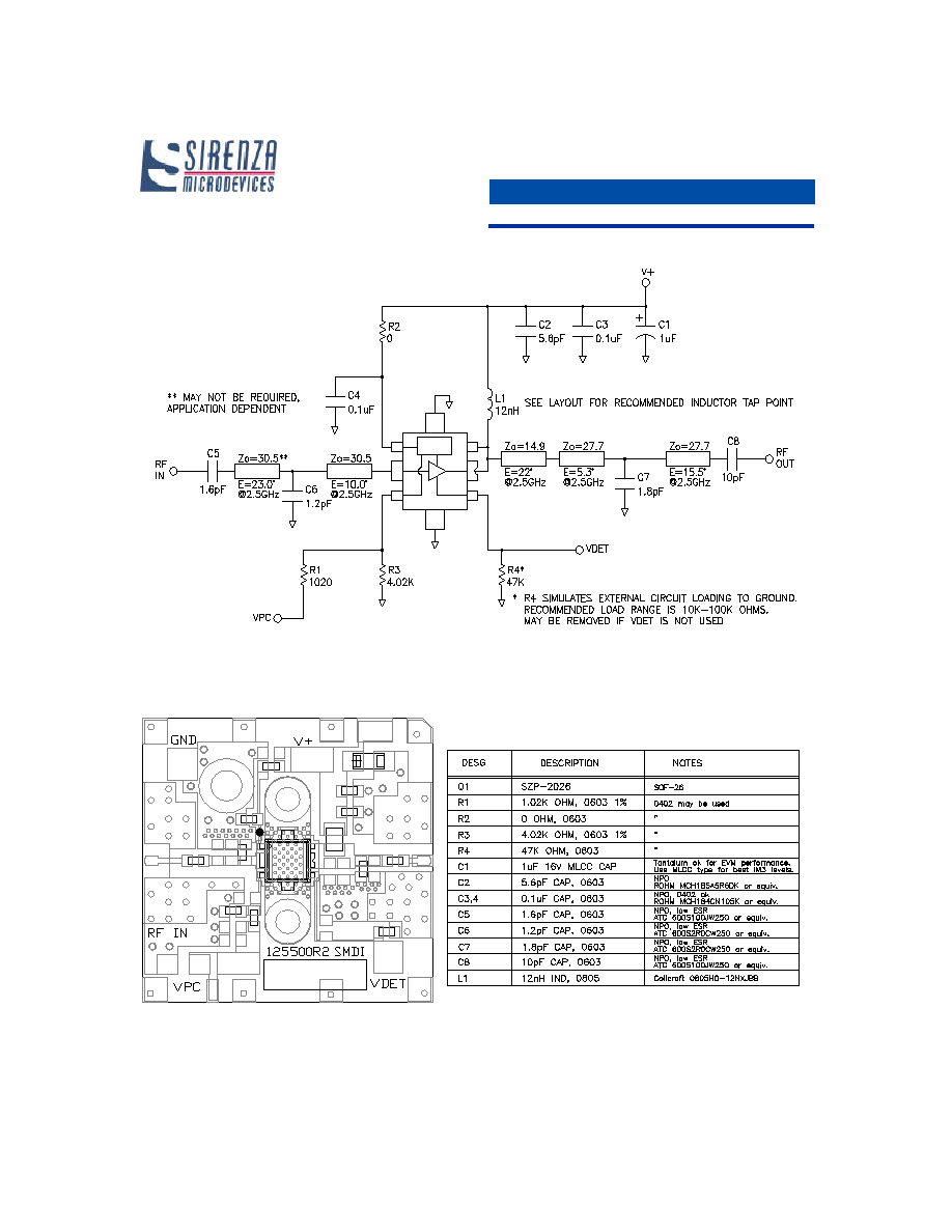
2.5-2.7 GHz Application Circuit For V+ = Vcc = Vpc = 5.0V
2.5-2.7GHz Evaluation Board Layout For V+ = Vcc = Vpc = 5.0V
Board material GETEK, 10mil thick, Dk=3.9, 2 oz. copper
C1
C2
C3
C4
R2
C8
C7
C6
C5
R1
L1
R3
R4
Q1
1
2
3
4
5
6
Bias
SZP-2026
303 South Technology Court Broomfield, CO 80021
Phone: (800) SMI-MMIC
http://www.sirenza.com
12
EDS-104611 Rev C
Preliminary
SZP-2026Z 2.2-2.7GHz 2W Power Amp
SPA
Part Number Ordering Information
Part Number
Reel Size
Devices/Reel
SZP-2026Z*
13"
3000
Part Symbolization
The part will be symbolized with "SZP-2026Z" to des-
ignate it as a RoHS green compliant product. Marking
designator will be on the top surface of the package.
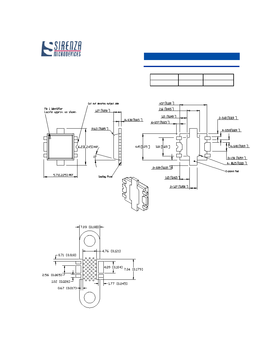
Recommended Metal Land Pattern (dimensions in mm [in]):
Package Outline Drawing (dimensions in mm [in]):
* Matte tin finish