The information provided herein is believed to be reliable at press time. Sirenza Microdevices assumes no responsibility for inaccuracies or omissions. Sirenza Microdevices assumes no responsibility for the use of this information, and all such
information shall be entirely at the user's own risk. Prices and specifications are subject to change without notice. No patent rights or licenses to any of the circuits described herein are implied or granted to any thrid party. Sirenza Microdevices
does not authorize or warrant any Sirenza Microdevices product for use in life-support devices and/or systems. Copyright 2003 Sirenza Microdevices, Inc. All worldwide rights reserved.
303 S. Technology Court,
Phone: (800) SMI-MMIC
http://www.sirenza.com
Broomfield, CO 80021
1
EDS-102932 Rev C
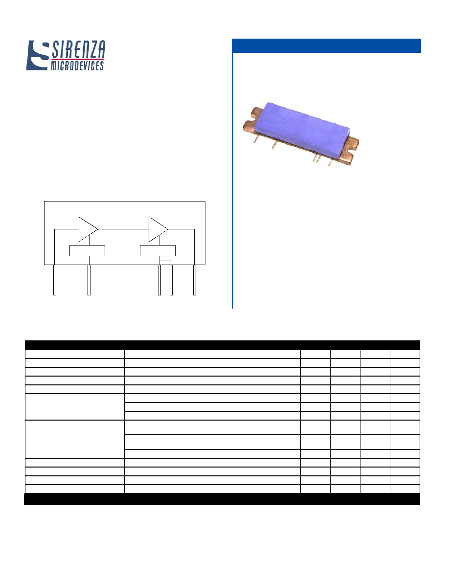
Sirenza Microdevices' XD010-24S-D2F 12W power module is a robust 2-
stage Class A/AB amplifier module for use in the driver stages of CDMA
RF power amplifiers. The power transistors are fabricated using Sirenza's
latest, high performance LDMOS process. This unit operates from a single
voltage and has internal temperature compensation of the bias voltage to
ensure consistant performance over the full temperature range. It is inter-
nally matched to 50 ohms.
Key Specifications
Symbol
Parameter
Unit
Min.
Typ.
Max.
Frequency
Frequency of Operation
MHz
1930
1990
P
1dB
Output Power at 1dB Compression
W
10
12
Gain
Gain at 1W Output Power
dB
26
28
Gain Flatness
Peak to Peak Gain Variation, 1930-1990MHz
dB
0.4
1.0
IRL
Input Return Loss 1W Output Power, 1930-1990MHz
dB
10
14
Efficiency
Drain Efficiency at 10W CW output
%
20
26
Drain Efficiency at 2W CDMA (Single Carrier IS-95, 9 Ch Fwd)
%
12
Drain Efficiency at 1W CDMA (Single Carrier IS-95, 9 Ch Fwd)
%
6.5
Linearity
ACPR at 1W CDMA Power Output (Single Carrier IS-95, 9 Ch
Fwd, Offset=750KHz, ACPR Integrated Bandwidth)
dB
-58
ALT-1 at 2W CDMA (Single Carrier IS-95, 9 Ch Fwd,
Offset=1980 KHz, ACPR Integrated Bandwidth)
dB
-70
3
rd
Order IMD at 10W PEP (Two Tone; 1MHz)
dBc
-27
-32
Delay
Signal Delay from Pin 1 to Pin 5
nS
2.9
Phase Linearity
Deviation from Linear Phase (Peak to Peak)
Deg
0.5
R
TH, j-l
Thermal Resistance Stage 1 (Junction to Case)
�C/W
11
R
TH, j-2
Thermal Resistance Stage 2 (Junction to Case)
�C/W
4
XD010-24S-D2F
1930-1990 MHz Class A/AB
12W CDMA Driver Amplifier
Product Features
Applications
�
50 W RF impedance
�
12W Output P
1dB
�
Single Supply Operation : Nominally 28V
�
High Gain: 28 dB at 1960 MHz
�
High Efficiency: 26% at 1960 MHz
�
Advanced, XeMOS LDMOS II FETS
�
Temperature Compensation
�
Base Station PA driver
�
Repeater
�
CDMA
�
GSM / EDGE
Product Description
Test Conditions: Z
in
= Z
out
= 50
, V
DD
= 28.0V, I
DQ1
= 230mA, I
DQ2
= 150mA, T
Flange
= 25�C
Functional Block Diagram
4
Temperature
Compensation
5
3
2
1
Stage 1
Stage 2
RF in
RF out
V
D1
D2
V
Temperature
Compensation
Case Flange = Ground

XD010-24S-D2F 1930-1990 MHz 12W Power Amp Module
303 S. Technology Court
Phone: (800) SMI-MMIC
http://www.sirenza.com
Broomfield, CO 80021
2
EDS-102932 Rev C
Pin Out Description
Pin #
Function
Description
1
RF Input
Module RF input. Care must be taken to protect against video transients that may damage the active devices.
2
V
D1
This is the bias feed for the 1
st
stage of the amplifier module. The gate bias is temperature compensated to maintain con-
stant current over the operating temperature range. See Note 1.
3,4
V
D2
This is the bias feed for the 2
nd
stage of the amplifier module. The gate bias is temperature compensated to maintain con-
stant current over the operating temperature range. See Note 1.
5
RF Output
Module RF output. Care must be taken to protect against video transients that may damage the active devices.
Flange
Gnd
Exposed area on the bottom side of the package needs to be mechanically attached to the ground plane of the board for
optimum thermal and RF performance. See mounting instructions for recommendation.
Simplified Device Schematic
Absolute Maximum Ratings
Parameters
Value
Unit
1
st
Stage Bias Voltage (V
D1
)
35
V
2
nd
Stage Bias Voltage (V
D2
)
35
V
RF Input Power
+20
dBm
Load Impedance for Continuous Operation
Without Damage
5:1
VSWR
Output Device Channel Temperature
+200
�C
Operating Temperature Range
-20 to +90
�C
Storage Temperature Range
-40 to
+100
�C
Operation of this device beyond any one of these limits may
cause permanent damage. For reliable continuous operation
see typical setup values specified in the table on page one.
Caution: ESD Sensitive
Appropriate precaution in handling, packaging
and testing devices must be observed.
Note 1:
The internally generated gate voltage is thermally compensated
to maintain constant quiescent current over the temperature
range listed in the data sheet. No compensation is provided for
gain changes with temperature. This can only be accomplished
with AGC external to the module.
Note 2:
Internal RF decoupling is included on all bias leads. No addi-
tional bypass elements are required, however some applica-
tions may require energy storage on the drain leads to
accommodate time-varying waveforms.
Note 3:
This module was designed to have its leads hand soldered to an
adjacent PCB. The maximum soldering iron tip temperature
should not exceed 700� C, and the soldering iron tip should not
be in direct contact with the lead for longer than 10 seconds.
Refer to app note AN060 (www.sirenza.com) for further installa-
tion instructions.
Quality Specifications
Parameter
Unit
Typical
ESD Rating
Human Body Model, JEDEC Document - JESD22-A114-B
V
8000
MTTF
85
o
C Baseplate, 200
o
C Channel
H
1.2 X 10
6
Temperature
Compensation
RF
in
1
Q1
Q2
2
3
5
RF
out
Case Flange = Ground
D1
V
V
D2
Temperature
Compensation
4
XD010-24S-D2F 1930-1990 MHz 12W Power Amp Module
303 S. Technology Court
Phone: (800) SMI-MMIC
http://www.sirenza.com
Broomfield, CO 80021
3
EDS-102932 Rev C
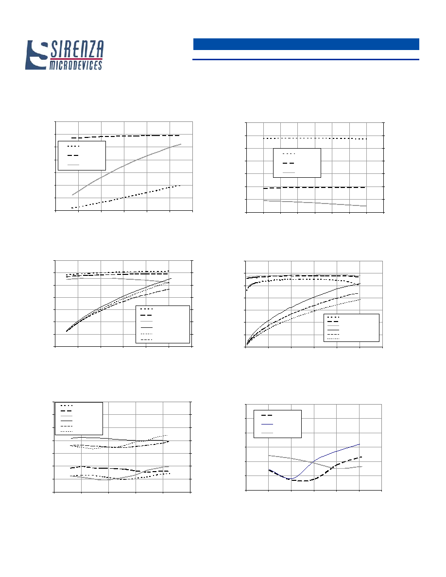
Two Tone IMD vs. Output Power and Temperature
Freq=1960, 1961 MHz, Vdd=28 V, T
Flange
=-20
o
C, 25
o
C, 90
o
C
-60
-50
-40
-30
-20
-10
0
0
1
2
3
4
5
6
Output Power, Avg (W)
IMD (dBc
)
IMD @ 25 C
IMD @ 90
IMD @ -20
ACPR and ALT1 vs. Output Power and Temperature
Freq=1960 MHz IS-95 Vdd=28 V, T
Flange
=-20�C, 25�C, 90�C
ACPR 885 kHz, 30 kHz
ALT1 1.25 MHz, 30 kHz
-70
-60
-50
-40
-30
-20
-10
0
0
0.5
1
1.5
2
2.5
Output Power (W)
AC
PR
(d
B)
-100
-90
-80
-70
-60
-50
-40
-30
AL
T1
(d
B)
ACPR @ 25�C
ACPR @-20�C
ACPR @ 90�C
ALT1 @-20�C
ALT1 @ 25�C
ALT1 @ 90�C
Gain and Efficiency vs. Output Power and Temperature
Freq=1960 MHz, Vdd=28 V, T
Flange
=-20�C, 25�C, 90�C
0
5
10
15
20
25
30
35
0
2
4
6
8
10
12
Output Power (W)
Ga
in
(d
B)
0
5
10
15
20
25
30
35
E
f
f
i
ci
ency (%)
Gain @-20�C
Gain @ 25�C
Gain @ 90�C
Efficiency @-20�C
Efficiency @ 25�C
Efficiency @ 90�C
Gain, Efficiency and ACPR vs. Frequency
Freq=1960 MHz, Vdd=28 V, T
Flange
= 25�C
Output Power=2 Watts
0
5
10
15
20
25
30
35
1920
1930
1940
1950
1960
1970
1980
1990
2000
Frequency (MHz)
Gai
n
(dB), Effi
ci
ency (%)
-60
-55
-50
-45
-40
-35
-30
-25
AC
PR
(d
B)
Gain
Efficiency
ACPR
Gain, Output Power and Efficiency vs. Input Power
Freq=1960 MHz, Vdd=28 V, T
Flange
= 25�C
0
5
10
15
20
25
30
35
0
0.002
0.004
0.006
0.008
0.01
0.012
Input Power (W)
Ga
in
(d
B), Ou
tp
u
t
Po
w
e
r (W), Efficie
n
cy (%
)
Pout
Gain
Efficiency
Typical Performance Curves
Gain and Efficiency vs. Output Power and Voltage
Freq=1960 MHz, Vdd=24V, 28 V, 32 V T
Flange
= 25�C
0
5
10
15
20
25
30
35
0
2
4
6
8
10
12
Output Power (W)
Ga
in
(d
B), Effic
i
e
n
c
y
(%)
Gain @ 24 VDC
Gain @ 28 VDC
Gain @ 32 VDC
Efficiency @ 24 VDC
Efficiency @ 28 VDC
Efficiency @ 32 VDC
XD010-24S-D2F 1930-1990 MHz 12W Power Amp Module
303 S. Technology Court
Phone: (800) SMI-MMIC
http://www.sirenza.com
Broomfield, CO 80021
4
EDS-102932 Rev C
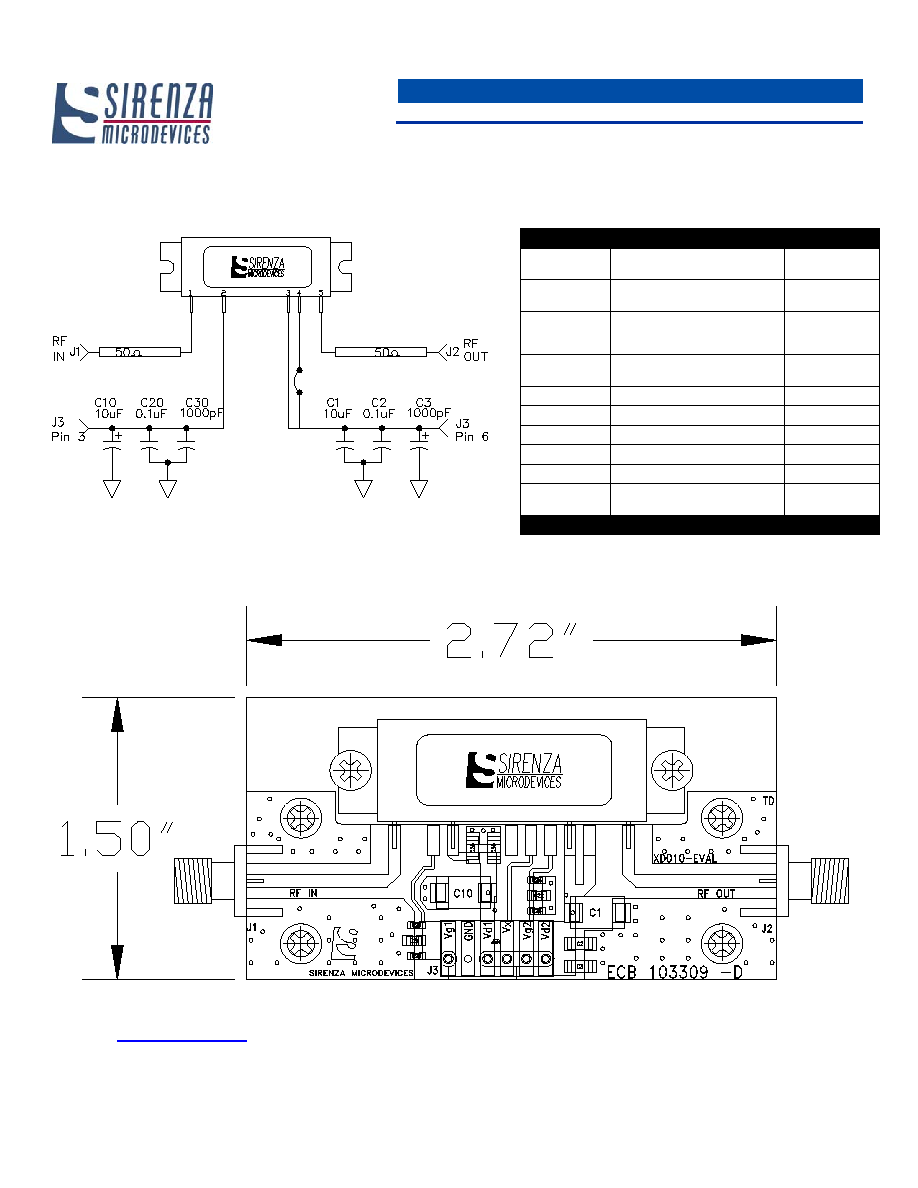
Test Board Schematic with module attachments shown
Test Board Layout
To receive Gerber files, DXF drawings, a detailed BOM, and assembly recommendations for the test board with fixture, contact applications
support at
support@sirenza.com.
Data sheet for evaluation circuit (XD010-EVAL) available from Sirenza website.
Component
Description
Manufacturer
PCB
Rogers 4350, e
r
=3.5
Thickness=30mils
Rogers
J1, J2
SMA, RF, Panel Mount Tab W /
Flange
Johnson
J3
MTA Post Header, 6 Pin, Rect-
angle, Polarized, Surface
Mount
AMP
C1, C10
Cap, 10mF, 35V, 10%, Tant,
Elect, D
Kemet
C2, C20
Cap, 0.1mF, 100V, 10%, 1206
Johanson
C3, C30
Cap, 1000pF, 100V, 10%, 1206
Johanson
C25, C26
Cap, 68pF, 250V, 5%, 0603
ATC
C21, C22
Cap, 0.1mF, 100V, 10%, 0805
Panasonic
C23, C24
Cap, 1000pF, 100V, 10%, 0603
AVX
Mounting
Screws
4-40 X 0.250"
Various
Test Board Bill of Materials
XD010-24S-D2F 1930-1990 MHz 12W Power Amp Module
303 S. Technology Court
Phone: (800) SMI-MMIC
http://www.sirenza.com
Broomfield, CO 80021
5
EDS-102932 Rev C
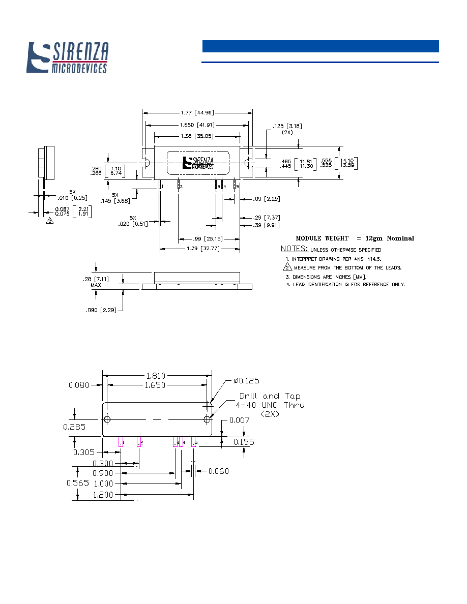
Package Outline Drawing
Recommended PCB Cutout and Landing Pads for the D2F Package
Note 3: Dimensions are in inches
Refer to Application note AN-060 "Installation Instructions for XD Module Series" for additional mounting info. App note availbale at at www.sirenza.com