The information provided herein is believed to be reliable at press time. Sirenza Microdevices assumes no responsibility for inaccuracies or ommisions.
Sirenza Microdevices assumes no responsibility for the use of this information, and all such information shall be entirely at the user's own risk. Prices and specifications are subject to change without
notice. No patent rights or licenses to any of the circuits described herein are implied or granted to any third party. Sirenza Microdevices does not authorize or warrant any Sirenza Microdevices product
for use in life-support devices and/or systems.
Copyright 2003 Sirenza Microdevices, Inc. All worldwide rights reserved.
522 Almanor Ave., Sunnyvale, CA 94085
Phone: (800) SMI-MMIC
http://www.sirenza.com
1
EDS-102938 Rev B
Prelimi nary
The XD010-42S-D4F 10W power module is a 2-
stage Class A amplifier module for use in the driver
stages of linear RF power amplifiers of cellular base
stations. The power transistors are fabricated using
Sirenza's latest, high performance LDMOS process.
This unit operates from a single voltage and has
internal temperature compensation of the bias volt-
age to ensure stable performance over the full tem-
perature range.
Key Specifications
Parameter
Description: Test Conditions
Z
in
= Z
out
= 50
, V
DD
= 28.0V, I
DD1
= 230mA,
I
DD2
= 700mA, T
Flange
= 25�C
Unit
Min.
Typ.
Max.
Frequency
Frequency of Operation
MHz
869
894
P
1dB
Output Power at 1dB Compression, 880 MHz
W
8
Gain
Gain at 1W Output Power
dB
30
Gain Flatness
Over Frequency at 1W Output (CW)
dB
0.4
IRL
Input Return Loss at 1W Output (CW) (50
Ref)
dB
20
Efficiency
Drain Efficiency at 8W CW Output
%
24
Drain Efficiency at 1W CDMA (Single Carrier IS-95)
%
3.5
Linearity
ACPR at 1W CDMA Output (Single Carrier IS-95)
dB
-50
ALT-1 PR at 1W CDMA (Single Carrier IS-95)
dB
-75
3
rd
Order IMD at 8W PEP (Two Tone 1MHz Spacing)
dBc
-30
3
rd
Order IMD at 1W PEP (Two Tone 1MHz Spacing)
dBc
-50
Delay
Signal Delay from Pin 1 to Pin 4
nS
3.9
Phase Linearity
Deviation from Linear Phase (Peak to Peak)
Deg
0.5
R
TH, j-l
Thermal Resistance Stage 1 (Junction to Case)
�C/W
11
R
TH, j-2
Thermal Resistance Stage 2 (Junction to Case)
�C/W
4
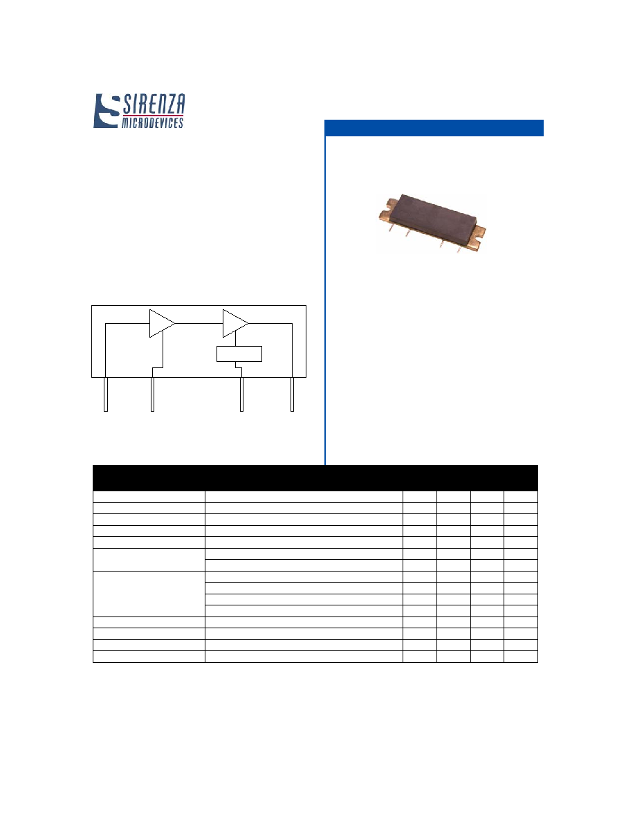
Functional Block Diagram
XD010-42S-D4F
869-894 MHz Class A
10W Power Amplifier Module
Product Features
Applications
�
50 W RF impedance
�
8W Output P
1dB
Typical
�
Single Voltage Operation
�
High Gain: 30 dB Typical
�
Advanced, XeMOS II LDMOS FETS
�
Temperature Compensation
�
Base Station PA driver
�
Repeater
�
CDMA
�
GSM / EDGE
Product Description
S tage 2
Tem perature
C om pensation
28 V
D C
2
C ase Flange = G round
R F in
28 V
1
S tage 1
D C
R F out
3
4
522 Almanor Ave., Sunnyvale, CA 94085
Phone: (800) SMI-MMIC
http://www.sirenza.com
2
EDS-102938 Rev B
Preliminary
XD010-42S-D4F 869-894 MHz 10W Amp
Pin Out Description
Pin #
Function
Description
1
RF Input
Module RF input. This pin is internally connected to DC ground. Do not apply DC voltages to the RF leads.
Care must be taken to protect against video transients that may damage the active devices.
2
V
DD1
This is the bias feed for the 1
st
stage of the amplifier module.
3
V
DD2
This is the bias feed for the 2
nd
stage of the amplifier module. The gate bias is temperature compensated to
maintain constant current over the operating temperature range. See Note 1.
4
RF Output
Module RF output. This pin is internally connected to DC ground. Do not apply DC voltages to the RF leads.
Care must be taken to protect against video transients that may damage the active devices.
Flange
Gnd
Exposed area on the bottom side of the package needs to be mechanically attached to the ground plane of the
board for optimum thermal and RF performance. See mounting instructions for recommendation.
Simplified Device Schematic
Absolute Maximum Ratings
Parameters
Value
Unit
1
st
Stage Bias Voltage (V
DD1
)
35
V
2
nd
Stage Bias Voltage (V
DD2
)
35
V
RF Input Power
+20
dBm
Load Impedance for Continuous Operation
Without Damage
5:1
VSWR
Base Plate Temperature: Operating with no
RF present
90
�C
Output Device Channel Temperature
+200
�C
Lead Temperature During Solder Reflow
+210
�C
Operating Temperature Range
-20 to +90
�C
Storage Temperature Range
-40 to +100
�C
Operation of this device beyond any one of these limits may
cause permanent damage. For reliable continuous operation see
typical setup values specified in the table on page one.
Caution: ESD Sensitive
Appropriate precaution in handling, packaging
and testing devices must be observed.
Note 1:
The internal generated gate voltage is ther-
mally compensated to maintain constant qui-
escent current over the temperature range
listed in the data sheet. No compensation is
provided for gain changes with temperature.
This can only be provided with AGC external
to the module.
Note 2:
Internal RF decoupling is included on all bias
leads. No additional bypass elements are
required, however some applications may
require energy storage on the drain leads to
accommodate time-varying waveforms.
Bias Network
RF
in
1
Q1
Case Flange = Ground
Temperature
Compensation
Q2
Vdd1
2
3
Vdd2
4
RF
out
522 Almanor Ave., Sunnyvale, CA 94085
Phone: (800) SMI-MMIC
http://www.sirenza.com
3
EDS-102938 Rev B
Preliminary
XD010-42S-D4F 869-894 MHz 10W Amp
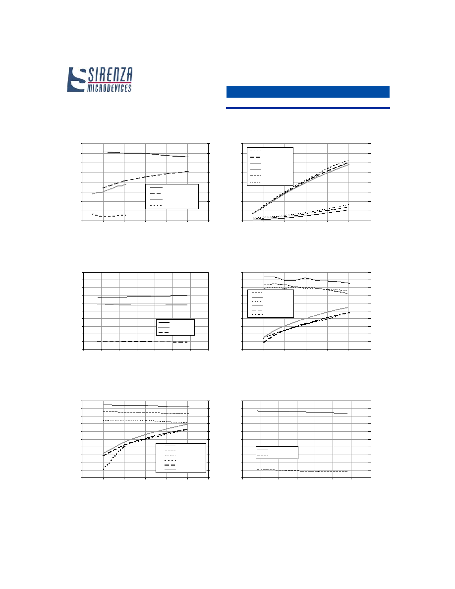
Gain, IMD, ACP, ALT1 vs. Output Power Freq=881 MHz,
Vdd=28V, T
Flange
=25
o
C, IS-95 ADJ BW=30KHz @ 750 KHz
ALT1 BW=30KHz @1980 KHz, IMD @ 1 MHz spacing
23
24
25
26
27
28
29
30
31
0
1
2
3
4
5
6
Output Power (W)
Gain (dB)
-80
-70
-60
-50
-40
-30
-20
-10
0
AC
P(dB),
ALT
1(dB),
I
M
D
(dBc
)
Two Tone Gain
IMD 1MHz Spacing
ACP
ALT1
Two Tone IMD, ACP, ALT1 vs. Frequency
Output Power=1 Watt, Vdd=28 V, T
Flange
=25
o
C
IS95 ADJ BW= 30 KHz@ 750 KHz
ALT1 BW= 30 KHz@1980 KHz, IMD @1 MHz spacing.
-80
-75
-70
-65
-60
-55
-50
-45
-40
-35
-30
865
870
875
880
885
890
895
900
Frequency (MHz)
AC
PR
(dB),
ALT
1
(dB),
I
M
D
(dBc
)
Two Tone IMD
ACP
ALT1
Gain and IMD vs. Output Power and Temperature
Freq=881 MHz, Vdd=28 V, T
Flange
=-20
o
C, 25
o
C, 90
o
C
13
15
17
19
21
23
25
27
29
31
33
0
1
2
3
4
5
6
Output Power (W)
Gain (dB)
-60
-55
-50
-45
-40
-35
-30
-25
-20
-15
-10
IMD (d
B
c
)
Gain @-20�C
Gain @ 25�C
Gain @ 90�C
IMD @-20�C
IMD @ 25�C
IMD @ 90�C
Gain and IMDs vs. Output Power and Voltage
Freq=881 and 882 MHz, Vdd=24 V, 28 V, 32 V
T
Flange
=25
o
C
21
22
23
24
25
26
27
28
29
30
31
0
1
2
3
4
5
6
Output Power (W)
Gain (dB)
-50
-45
-40
-35
-30
-25
-20
-15
-10
-5
0
IMD (d
B
c
)
Gain @ 24 Volts
Gain @ 28 Volts
Gain @ 32 Volts
IMD @ 24 Volts
IMD @ 28 Volts
IMD @ 32 Volts
Gain and Input Return Loss vs. Frequency
Output Power=1 Watt, Vdd=28 V, T
Flange
=25
o
C
22
23
24
25
26
27
28
29
30
31
32
865
870
875
880
885
890
895
900
Frequency (MHz)
Gain (dB)
-24
-23
-22
-21
-20
-19
-18
-17
-16
-15
-14
I
nput
R
e
t
u
rn Los
s
(dB)
Gain
Input Return Loss
Efficiency and Idd vs. Output Power and Temperature
Freq=881 MHz, Vdd=28 V, T
Flange
=-20
o
C, 25
o
C, 90
o
C
0
5
10
15
20
25
30
35
40
0
2
4
6
8
10
12
Output Power (W)
E
ffi
ci
e
n
cy (
%
)
0.9
1.1
1.3
1.5
1.7
1.9
2.1
2.3
2.5
Id
d
(
A
mp
s)
Efficiency @-20�C
Efficiency @25�C
Efficiency @90�C
Id @-20�C
Id @ 25�C
Id @ 90�C
522 Almanor Ave., Sunnyvale, CA 94085
Phone: (800) SMI-MMIC
http://www.sirenza.com
4
EDS-102938 Rev B
Preliminary
XD010-42S-D4F 869-894 MHz 10W Amp
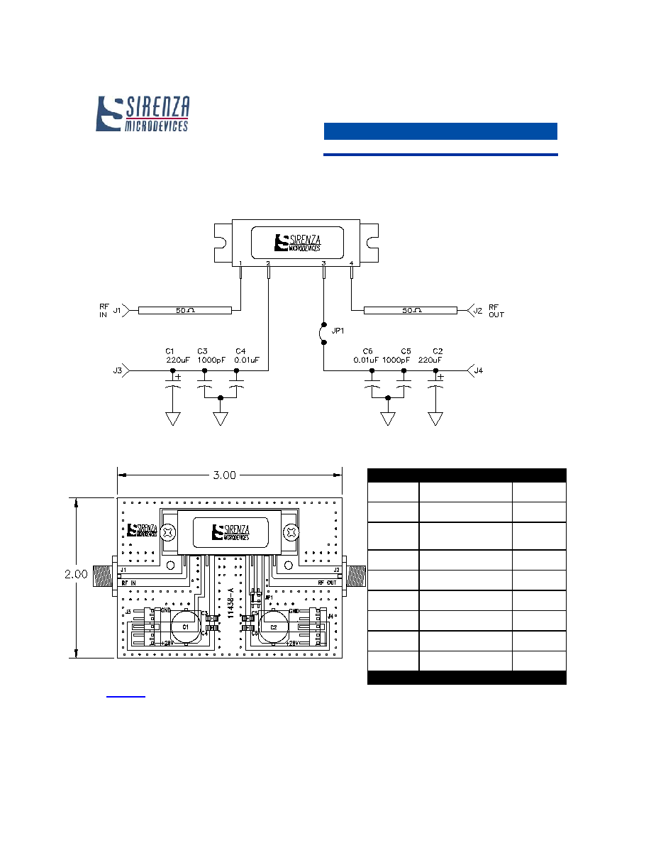
Test Board Schematic with module attachments shown
Test Board Layout and Bill of Materials
Component
Description
Manufacturer
PCB
Rogers 4350, e
r
=3.5
Thickness=30mils
Rogers
J1, J2
SMA, RF, Panel Mount
Tab W / Flange
AMP
J3, J4
MTA Post Header, 5 Pin,
Rectangle, Polarized,
Surface Mount
AMP
C1, C2
Cap, 220mF 50V, -40 to
85
o
C, Electrolytic, G
Panasonic
C4, C6
Cap, 0.01mF, 100V, 10%,
1206
Johanson
C3, C5
Cap, 1000pF, 100V, 10%,
1206
Johanson
JP1 Header
SMT Header, Low Profile,
2mm
Specialty
Electronics
JP1 Shunt
Shunt, Mate to Header,
2mm
Specialty
Electronics
Mounting
Screws
4-40 X 0.250"
Various
To download Gerber files, DXF drawings, a detailed BOM, and
assembly recommendations for the test board with fixture
click here

522 Almanor Ave., Sunnyvale, CA 94085
Phone: (800) SMI-MMIC
http://www.sirenza.com
5
EDS-102938 Rev B
Preliminary
XD010-42S-D4F 869-894 MHz 10W Amp
Package Outline Drawing
Recommended PCB Cutout and Landing Pads for the D4F Package
Note 3: Dimensions are in inches