 | –≠–ª–µ–∫—Ç—Ä–æ–Ω–Ω—ã–π –∫–æ–º–ø–æ–Ω–µ–Ω—Ç: ST2006 | –°–∫–∞—á–∞—Ç—å:  PDF PDF  ZIP ZIP |

ST
Sitronix
ST2006
PRELIMINARY
6K ROM Microcontroller with 128 Dot LCD Driver
Notice: This is not a final specification. Some parameters are subject to change.
Ver 1.21
1/39
2003
/7/4
1
1
.
.
F
F
E
E
A
A
T
T
U
U
R
R
E
E
S
S
8-bit static pipeline CPU
ROM: 6K x 8 bits
RAM: 96 x 8 bits (data + stack)
Operation voltage : 2.4V~3.4V
12 CMOS Bi-directional bit programmable I/O pins
8 Output pins (Shared with LCD segment)
Hardware de-bounce option for Port-A interrupt
Bit programmable PULL-UP for input port
Timer/Counter
:
- One 8-bit timer / 16-bit event counter
- One 8-bit BASE timer
Four powerful interrupt sources :
- External interrupt (edge trigger)
- TIMER1 interrupt
- BASE timer interrupt
- PORTA[7~0] interrupt (transition trigger)
16-level
deep
stack
Dual clock source :
- OSCX: Crystal oscillator: 32.768K Hz
- OSC: RC oscillator 500K ~ 2M Hz
Build-in oscillator with warm-up timer
LCD driver programmable duty :
- 128 (4x32) dots (1/4 duty, 1/3 bias)
- 96 (3x32) dots (1/3 duty, 1/2 bias)
Programmable Sound Generator (PSG) includes :
- Tone generator
- Noise generator
- 4 level volume control
Three power down modes :
- WAI0 mode
- WAI1 mode
- STP mode
Stand by current < 5uA
2
2
.
.
G
G
E
E
N
N
E
E
R
R
A
A
L
L
D
D
E
E
S
S
C
C
R
R
I
I
P
P
T
T
I
I
O
O
N
N
ST2006 is a low-cost, high-performance, fully static, 8-bit
microcontroller designed with CMOS silicon gate
technology. It comes with 8-bit pipeline CPU core, SRAM,
timer, LCD driver, I/O port, PSG and mask program ROM. A
build-in dual oscillator is specially integrated to enhance
chip performance. For handheld equipment and consumer
applications. Such as watch, calculator, LCD game and IR
remote control.
ST2006
Ver 1.21
2/38
2003/
7/4
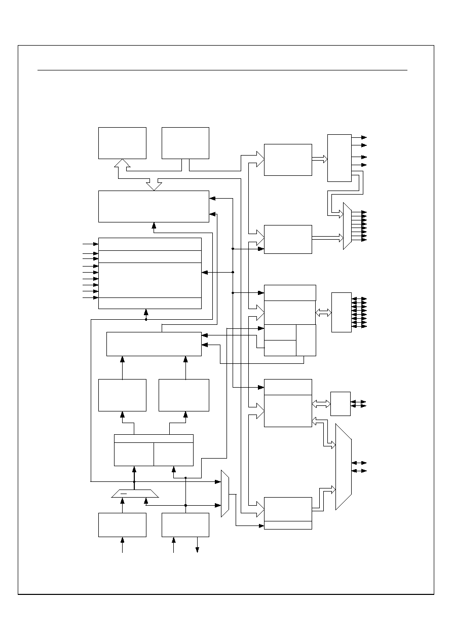
3
3
.
.
B
B
L
L
O
O
C
C
K
K
D
D
I
I
A
A
G
G
R
R
A
A
M
M
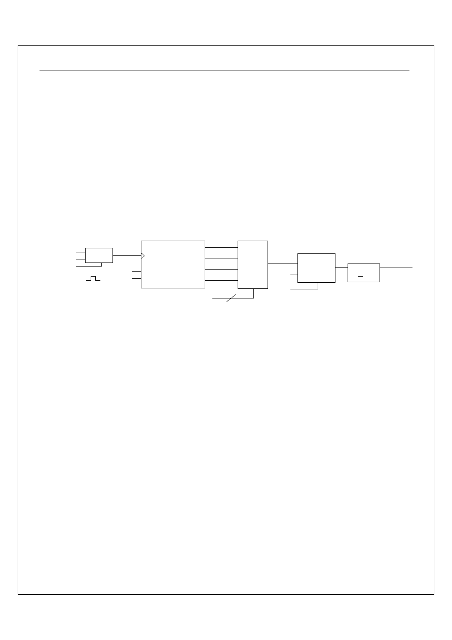
CPU
96 x 8
RAM
6K x 8
ROM
32 x 4
LCD RAM
LCD
Driver
PA
Port A
Pull_up A
controller
EXT.
INT
Pull_up B
controller
Port B
PSG
PSG clock
Reset & Warm_up Timer
Interrupt controller
Base Timer
Timer 1 &
Event counter
Prescaler
PRES
PREW
RC oscillator
32.768K
oscillator
MUX
Segment
Output
Hardware
Debounce
Port A
INT
System controller
Power down controller
PA0
PA1
PA2
PA3
PA4
PA5
PA6
PA7
PB2
PB3
SEG0
SEG1
SEG2
SEG3
COM0
COM3
SEG8
SEG31
: : :
: : :
VDD
Vss
V15
OSCI
OSCXO
OSCXI
2 MUX
:
M
U
X
PB
SYSCK
M
U
X
LCD voltage pump up
RESET
V30
V45
CUP1
CUP2
CUP3
PB
PB0
PB1
SEG4
SEG5
SEG6
SEG7
ST2006
Ver 1.21
3/38
2003/
7/4
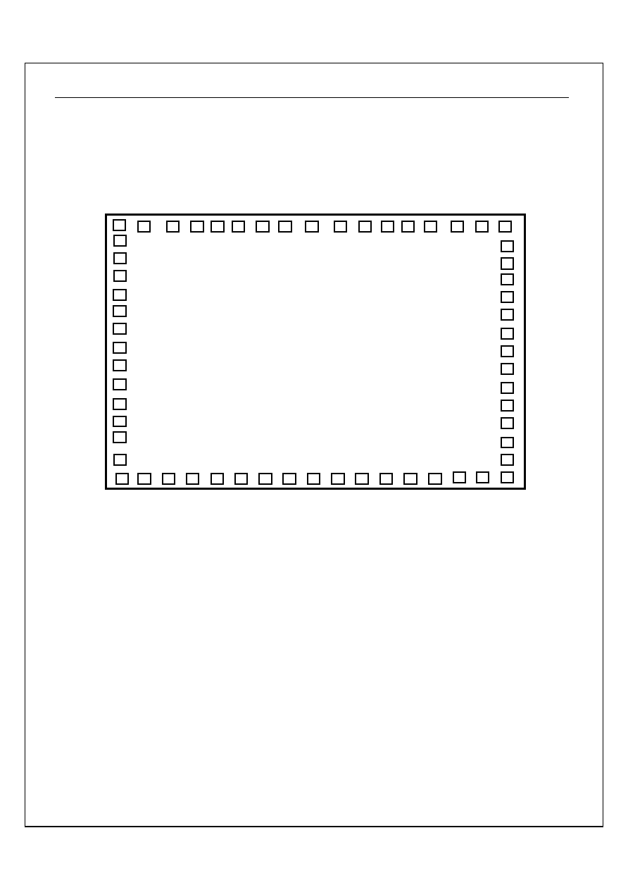
4
4
.
.
P
P
A
A
D
D
D
D
I
I
A
A
G
G
R
R
A
A
M
M
ST2006
SEG0
9
SEG1
23
22
21
20
19
18
1
2
3
4
5
6
7
8
10
53
52
51
45
44
43
42
41
40
39
38
37
36
35
VDD
CUP1
CUP2
COM 3
PA2
PB0
PB1
PB2
PB3
GND
OSCXO
RESET
OSCI
CUP3
V45
17
15
14
11
12
13
30
29
28
27
26
25
24
34
33
31
50
49
48
47
46
PA1
PA0/INT
X
SEG2
SEG 15
PA6
PA7
PA5
PA4
SEG 28
SEG 27
COM 0
COM 1
COM 2
PA3
SEG 29
SEG 31
SEG 30
SEG 26
SEG 25
SEG 24
SEG 23
SEG 22
SEG 21
SEG 20
SEG 19
SEG 18
SEG 17
SEG 16
SEG 14
SEG 13
SEG 12
SEG 11
SEG 10
SEG 9
54
55
SEG7
56
SEG6
57
SEG5
58
SEG4
59
SEG3
60
SEG 8
32
16
V30
V15
OSCXI
ST2006
Ver 1.21
4/38
2003/
7/4
5
5
.
.
P
P
A
A
D
D
D
D
E
E
S
S
C
C
R
R
I
I
P
P
T
T
I
I
O
O
N
N
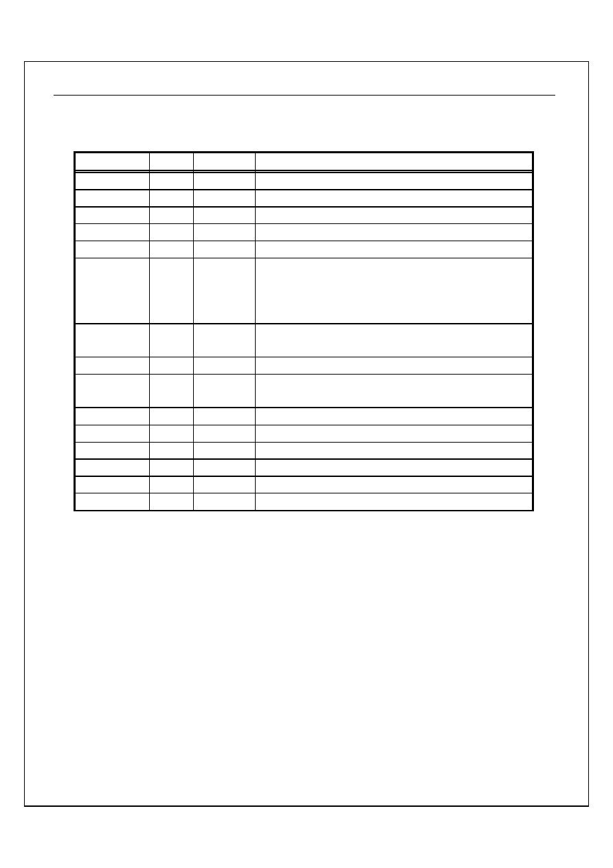
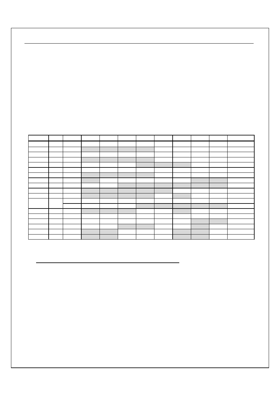
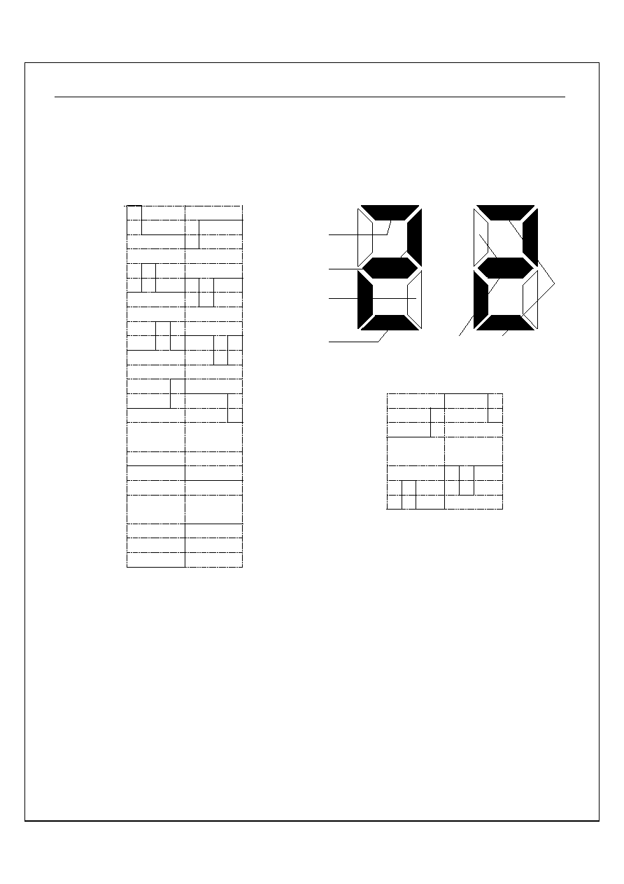
Designation Pad
# Type
Description
SEG 0 - 7
1~8
O
LCD Segment output or output port
SEG 8 - 31
37~60
O
LCD Segment output
COM 0 - 3
33~36
O
LCD Common output
RESET
17
I
Pad reset input (high active)
GND
20
P
Ground Input and chip substrate
PA0/INTX 32
I/O
I
I
I
Port-A bit programmable I/O
Edge-trigger Interrupt.
Transition-trigger Interrupt
Programmable Timer1 clock source
PA 1-7
25~31
I/O
I
Port-A bit programmable I/O
Transition-trigger Interrupt
PB 0-1
23, 24
I/O
Port-B bit programmable I/O
PB 2-3
21, 22
I/O
O
Port-B bit programmable I/O
PSG Output
V
DD
15 P
Power
supply
OSCXI
18
I
OSCX input pin, for 32768Hz crystal
OSCXO
19
O
OSCX output pin, for 32768Hz crystal
OSCI
16
I
OSC input pin, toward external resistor
CUP1~3
12~14
I
Voltage pump up capacitor
V15,V30,V45 9~11
I LCD
voltage
capacitor
Legend: I = input, O = output, I/O = input/output, P = power.

ST2006
Ver 1.21
5/38
2003/
7/4
6
6
.
.
C
C
P
P
U
U
7
0
A
7
0
Y
7
0
X
7
0
PCH PCL
8 7 6 5 4
0
1 0 0 0
S
Accumulator A
Index Register Y
Index Register X
Program Counter PC
Stack Pointer S
CPU REGISTER MODEL
6.1 Accumulator
(A)
The accumulator is a general purpose 8-bit register which
stores the results of most arithmetic and logic operations. In
addition, the accumulator usually contains one of the two
data words used in these operations.
6.2 Index Registers (X,Y)
There are two 8-bit Index Registers (X and Y) which may be
used to count program steps or to provide and index value to
be used in generating an effective address. When executing
an instruction which specifies indexed addressing, the CPU
fetches the OP code and the base address, and modifies the
address by adding the index register to it prior to performing
the desired operation. Pre or post-indexing of indirect
addresses is possible.
6.3 Stack Pointer (S)
The stack Pointer is an 8-bit register which is used to control
the addressing of the variable-length stack. It's range from
100H to 11FH total for 32 bytes (16-level deep). The stack
pointer is automatically incremented and decrement under
control of the microprocessor to perform stack
manipulations under direction of either the program or
interrupts (IRQ). The stack allows simple implementation of
nested subroutines and multiple level interrupts. The stack
pointer is initialized by the user's software.
6.4 Program Counter (PC)
The 16-bit Program Counter register provides the address
which step the microprocessor through sequential program
instructions. Each time the microprocessor fetches and
instruction from program memory, the lower byte of the
program counter (PCL) is placed on the low-order bits of the
address bus and the higher byte of the program counter
(PCH) is placed on the high-order 8 bits. The counter is
incremented each time an instruction or data is fetched from
program memory.
6.5 Status Register (P)
The 8-bit Processor Status Register contains seven status
flags. Some of the flags are controlled by the program,
others may be controlled both by the program and the CPU.
The instruction set contains a member of conditional branch
instructions which are designed to allow testing of these
flags.

ST2006
Ver 1.21
6/38
2003/
7/4
Bit 7
Bit 6
Bit 5
Bit 4
Bit 3
Bit 2
Bit 1
Bit 0
N V 1 B D I Z C
Bit 7: N : Signed flag by arithmetic
1 = Negative
0 = Positive
Bit 6: V : Overflow of signed Arithmetic flag
1 = Negative
0 = Positive
Bit 4: B : BRK interrupt flag
1 = BRK interrupt occur
0 = Non BRK interrupt occur
Bit 3: D : Decimal mode flag
1 = Decimal mode
0 = Binary mode
Bit 2: I : Interrupt disable flag
1 = Interrupt disable
0 = Interrupt enable
Bit 1: Z : Zero flag
1 = Zero
0 = Non zero
Bit 0: C : Carry flag
1 = Carry
0 = Non carry
TABLE 9-14: STATUS REGISTER (P)
ST2006
Ver 1.21
7/38
2003/
7/4
7
7
.
.
M
M
E
E
M
M
O
O
R
R
Y
Y
C
C
O
O
N
N
F
F
I
I
G
G
U
U
R
R
A
A
T
T
I
I
O
O
N
N
CONTROL
REGISTERS
No Use
User RAM
No Use
Stack RAM &
User RAM
Don't Use
LCD RAM
No Use
0000 H
003F H
0080 H
00BF H
0100 H
011F H
0200 H
021F H
E800 H
FFFF H
Program ROM
64 Bytes
64 Bytes
32 Bytes
32x4 Bits
6K Bytes
7.1 ROM
($E800~$FFFF)
The ST2006 has 6K bytes ROM for program, data and vector address.
Vector address mapping :
$FFFE
Software BRK operation interrupter.
$FFFC RESET
vector
$FFFA Reserved
$FFF8
INTX (PA0) edge interrupter.
$FFF6 Reserved
$FFF4 Reserved
$FFF2 Timer1
interrupter.
$FFF0 PORTA
transition
interrupter.
$FFEE Base
Timer
interrupter.
ST2006
Ver 1.21
8/38
2003/
7/4
7.2 RAM
7.2.1
DATA RAM ($0080~$00BF)
DATA RAM are organized in 64 bytes.
7.2.2
STACK RAM ($0100~$011F)
STACK RAM are organized in 32 bytes. It provides for a
maximum of 16-level subroutine stacks And can be used as
data memory.
7.2.3 LCD RAM ($0200~$021F)
Resident LCD-RAM, accessible through write and read
instructions, is organized in 32x4 bits for 32x4 LCD display.
Note that this area can also be used as data memory.
The RAM mapping includes Control Registers, Data RAM, Stack RAM and LCD RAM.
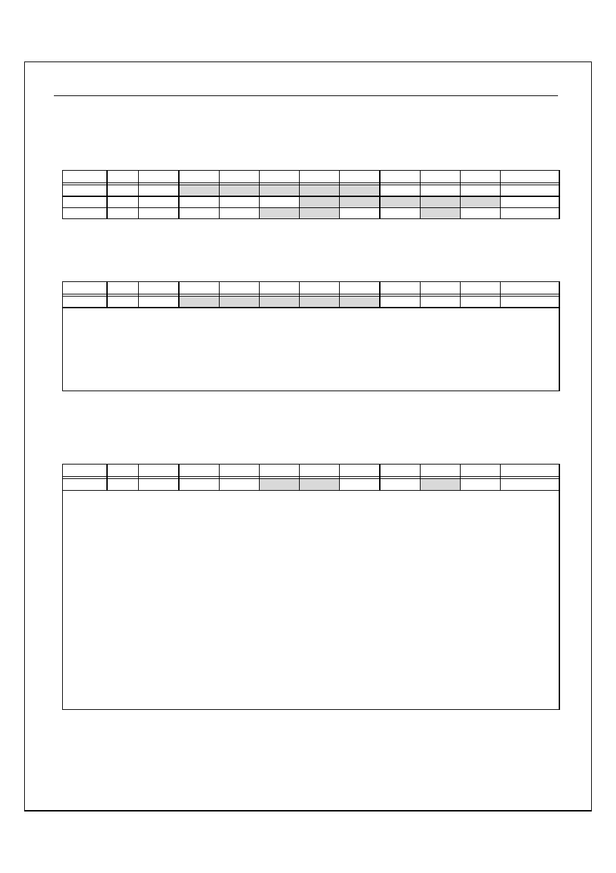
Address Name R/W
Bit 7
Bit 6
Bit 5
Bit 4
Bit 3
Bit 2
Bit 1
Bit 0
Default
$000 PA
R/W PA[7] PA[6] PA[5] PA[4] PA[3] PA[2] PA[1] PA[0] 1111
1111
$001 PB
R/W
-
-
-
-
PB[3]
PB[2]
PB[1]
PB[0]
- - - - 1111
$008 PCA R/W PCA[7] PCA[6] PCA[5] PCA[4] PCA[3] PCA[2] PCA[1] PCA[0] 0000
0000
$009 PCB R/W
-
-
-
-
PCB[3] PCB[2] PCB[1] PCB[0] - - - - 0000
$00F PMCR R/W PULL PDBN
INTEG -
-
-
PSGO
PSGB
100 - - -00
$012 PSGL W PSG[7] PSG[6] PSG[5] PSG[4] PSG[3] PSG[2] PSG[1] PSG[0] 0000
0000
$013 PSGH W
-
-
-
-
PSG[11] PSG[10] PSG[9] PSG[8] - - - - 0000
$016 PSGC W
-
PCK[2] PCK[1] PCK[0] PRBS C1EN
-
-
-000 00- -
$017 VOL
W VOL[1]
VOL[0] -
-
-
-
-
-
00- - - - - -
$020 LCK
W
-
-
-
-
-
LCK[2] LCK[1] LCK[0]
- - - - -100
$021 BTM
W
-
-
-
- BTM[3] -
BTM[1] BTM[0]
- - - - 0-00
R
PRS[7] PRS[6] PRS[5] PRS[4] PRS[3] PRS[2] PRS[1] PRS[0] 0000
0000
$023 PRS
W SRES SENA SENT
-
-
-
-
-
000 - - - - -
$026 T1M R/W
-
-
- T1M[4]
T1M[3] -
T1M[1] T1M[0]
- - -0 0-00
$027 T1C
R/W T1C[7] T1C[6] T1C[5] T1C[4] T1C[3] T1C[2] T1C[1] T1C[0] 0000
0000
$030 SYS R/W XSEL OSTP XSTP XBAK WSKP WAIT
-
-
0000 00- -
$03A LCTL W LPWR
BLANK -
- SEGO1
SEGO0 -
DUTY
00- - 00-0
$03C IREQ R/W
-
- IRBT
IRPT
IRT1 -
-
IRX
- - 00 0- -0
$03E IENA R/W
-
- IEBT
IEPT
IET1 -
-
IEX
- - 00 0- -0
Note: 1. Some addresses of I/O area, $2~$7, $A~$E, $10~$11, $14~$15, $18~$1F, $22, $24~$25, $28~$2F, $31~$39, $3B,
$3D, $3F are no used.
2. User should never use undefined addresses and bits.
3. Do not use Bit instructions for write-only registers, such as RMBx, SMBx....
TABLE 9-15: CONTROL REGISTERS ($0000~$003E)
ST2006
Ver 1.21
9/38
2003/
7/4
8
8
.
.
I
I
N
N
T
T
E
E
R
R
R
R
U
U
P
P
T
T
S
S
8.1 Interrupt
description
BRK
Instruction `BRK' will cause software interrupt when interrupt
disable flag (I) is cleared. Hardware will push `PC', `P'
Register to stack and set interrupt disable flag (I). Program
counter then will be loaded with the BRK vector from
locations $FFFE and $FFFF.
RESET
A negative transition of RESET pin will enable an
initialization sequence. After the system's operating, a low
on this line of a least two clock cycles will cease ST2006
activity. When a positive edge is detected, there is an
initialization sequence lasting for six clock cycles. Then the
interrupt mask flag is set, the decimal mode is cleared and
the program counter will be loaded with the restart vector
from locations $FFFC (low byte) and $FFFD (high byte).
This is the start location for program control. This input
should be high in normal operation.
INTX interrupt
The IRX (INTX interrupt request) flag will be set while INTX
edge signal occurs. The INTX interrupt will be active once
IEX (INTX interrupt enable) is set, and interrupt mask flag is
cleared. Hardware will push `PC', `P' Register to stack and
set interrupt mask flag (I). Program counter will be loaded
with the INTX vector from locations $FFF8 and $FFF9.
T1 interrupt
The IRT1 (TIMER1 interrupt request) flag will be set while T1
overflows. With IET1 (TIMER1 interrupt enable) being set,
the T1 interrupt will be executed, and interrupt mask flag will
be cleared. Hardware will push `PC', `P' Register to stack
and set interrupt mask flag (I). Program counter will be
loaded with the T1 vector from locations $FFF2 and $FFF3.
PT interrupt
The IRPT (Port-A interrupt request) flag will be set while
Port-A transition signal occurs. With IEPT (PT interrupt
enable)being set, the PT interrupt will be execute, and
interrupt mask flag will be cleared. Hardware will push `PC',
`P' Register to stack and set interrupt mask flag (I). program
counter will be loaded with the PT vector from locations
$FFF0 and $FFF1.
BT interrupt
The IRBT (Base timer interrupt request) flag will be set when
Base Timer overflows. The BT interrupt will be executed
once the IEBT (BT interrupt enable) is set and the interrupt
mask flag is cleared. Hardware will push `PC', `P' Register
to stack and set interrupt mask flag (I). Program counter will
be loaded with the BT vector from locations $FFEE and
$FFEF.
Name
Name
Name
Name Signal
Signal
Signal
Signal Vector
address
Vector address
Vector address
Vector address
Priority
Comment
Comment
Comment
Comment
BRK Internal $FFFF,$FFFE 6
Software BRK operation vector
RESET External
$FFFD,$FFFC
1
RESET vector
-
-
$FFFB,$FFFA
-
Reserved
INTX External $FFF9,$FFF8 2
PA0 edge interrupt
-
-
$FFF7,$FFF6
-
Reserved
-
-
$FFF5,$FFF4
-
Reserved
T1 INT/EXT $FFF3,$FFF2 3
Timer1 interrupt
PT External $FFF1,$FFF0 4
Port-A transition interrupt
BT Internal $FFEF,$FFEE 5
Base Timer interrupt
TABLE 9-16: PREDEFINED VECTORS FOR INTERRUPT
ST2006
Ver 1.21
10/38
2003/
7/4
8.2 Interrupt
request
clear
Interrupt request flag can be cleared by two methods. One is
to write "0" to IENA, the other is to initiate the interrupt
service routine when interrupt occurs. Hardware will
automatically clear the Interrupt flag.
Address Name R/W
Bit 7
Bit 6
Bit 5
Bit 4
Bit 3
Bit 2
Bit 1
Bit 0
Default
$03C IREQ R/W
-
- IRBT
IRPT
IRT1 -
-
IRX
- - 00 0--0
Bit 5: IRBT: Base Timer Interrupt Request bit
1 = Time base interrupt occurs
0 = Time base interrupt doesn't occur
Bit 4: IRPT: Port-A Interrupt Request bit
1 = Port-A transition interrupt occurs
0 = Port-A transition interrupt doesn't occur
Bit 3: IRT1: Timer1 Interrupt Request bit
1 = Timer1 overflow interrupt occurs
0 = Timer1 overflow interrupt doesn't occur
Bit 0: IRX: INTX Interrupt Request bit
1 = INTX edge interrupt occurs
0 = INTX edge interrupt doesn't occur
Address Name R/W
Bit 7
Bit 6
Bit 5
Bit 4
Bit 3
Bit 2
Bit 1
Bit 0
Default
$03E IENA R/W
-
- IEBT
IEPT
IET1 -
-
IEX
- - 00 0--0
Bit 5: IEBT: Base Timer Interrupt Enable bit
1 = Time base interrupt enable
0 = Time base interrupt disable
Bit 4: IEPT: Port-A Interrupt Enable bit
1 = Port-A transition interrupt enable
0 = Port-A transition interrupt disable
Bit 3: IET1: Timer1 Interrupt Enable bit
1 = Timer1 overflow interrupt enable
0 = Timer1 overflow interrupt disable
Bit 0: IEX: INTX Interrupt Enable bit
1 = INTX edge interrupt enable
0 = INTX edge interrupt disable
TABLE 9-17: INTERRUPT REQUEST REGISTER (IREQ)
TABLE 9-18: INTERRUPT ENABLE REGISTER (IENA)
ST2006
Ver 1.21
11/38
2003/
7/4
9
9
.
.
I
I
/
/
O
O
P
P
O
O
R
R
T
T
S
S
9.1 General
Function
ST2006 has three I/O ports, PORT-A, PORT-B,
SEGMENT-PORT. In total, ST2006 provides for a maximum
of 18 I/O pins with SEGMENT-PORT being programmed as
output ports. For detail pin assignment, please refer to
TABLE 9-19: :
PORT NAME
PAD NAME
PAD
NUMBER
PIN
TYPE
FEATURE
PA0/INTX 32 I/O
PA1 31
I/O
PA2 30
I/O
PA3 29
I/O
PA4 28
I/O
PA5 27
I/O
PA6 26
I/O
PORTA
PA7 25
I/O
programmable input/output pin
PB0 24
I/O
PB1 23
I/O
PB2 22
I/O
PORTB
PB3 21
I/O
programmable input/output pin
SEG0 8
O
SEG1 7
O
SEG2 6
O
SEG3 5
O
These 4 segment pins can be programmed as output
ports.
SEG4 4
O
SEG5 3
O
SEG6 2
O
SEGMENT
PORT
SEG7 1
O
These 4 segment pins can be programmed as output
ports.
TABLE 9-19: I/O DESCRIPTION
ST2006
Ver 1.21
12/38
2003/
7/4
9.2 PORT-A
Port- A is a bit-programmable bi-direction I/O port, which is
controlled by PCA register. It provides user with bit
programmable pull-up MOS, interrupt debounce and
interrupt edge selection(PA0 only).
Address Name R/W
Bit 7
Bit 6
Bit 5
Bit 4
Bit 3
Bit 2
Bit 1
Bit 0
Default
$000 PA
R/W PA[7] PA[6] PA[5] PA[4] PA[3] PA[2] PA[1] PA[0] 1111
1111
$008 PCA R/W PCA[7] PCA[6] PCA[5] PCA[4] PCA[3] PCA[2] PCA[1] PCA[0] 0000
0000
$00F PMCR R/W PULL PDBN
INTEG -
-
-
PSG0
PSGB
100 - - -00
$03C IREQ R/W
-
-
IRBT IRPT IRT1
-
-
IRX
- - 00 0- -0
$03E IENA R/W
-
-
IEBT IEPT IET1
-
-
IEX
- - 00 0- -0
1.1.1 PORT-A
I/O
control
Direction of Port-A is controlled by PCA. Every bit of
PCA[7-0] is mapped to the I/O direction of PA[7-0]
correspondingly with"1" for output mode, and "0" for input
mode.
Address Name R/W
Bit 7
Bit 6
Bit 5
Bit 4
Bit 3
Bit 2
Bit 1
Bit 0
Default
$008 PCA R/W PCA[7] PCA[6] PCA[5] PCA[4] PCA[3] PCA[2] PCA[1] PCA[0] 0000
0000
Bit 7~0: PCA[7~0] : Port-A directional bits
1 = Output mode
0 = Input mode
TABLE 9-110: SUMMARY FOR PORT-A REGISTERS
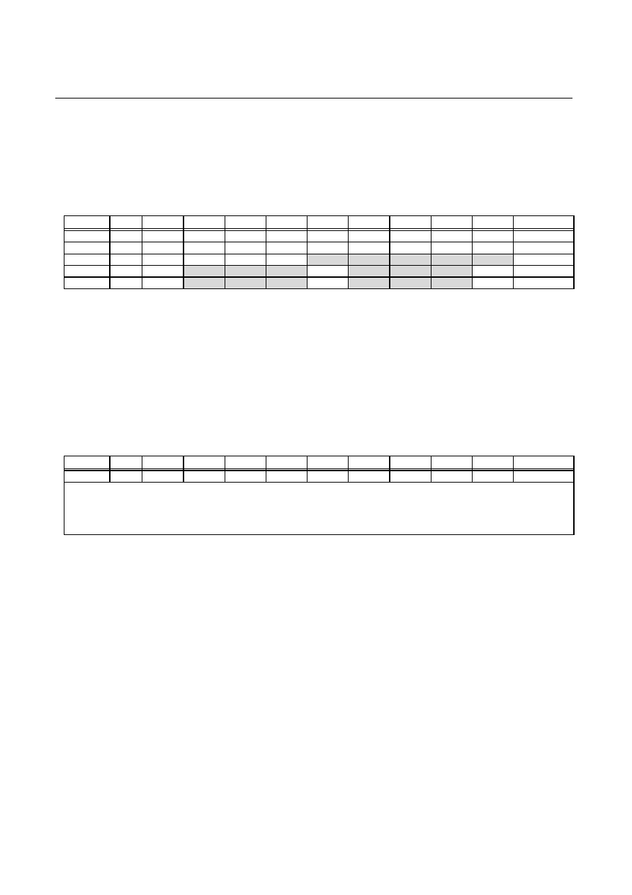
TABLE 9-8: PORT-A CONTROL REGISTER (PCA)

ST2006
Ver 1.21
13/38
2003/
7/4
9.2.2 PORT-A
PULL-UP
OPTION
PORT-A contains pull-up MOS transistors controlled by
software. When an I/O is used as an input, the ON/OFF of
the pull-up MOS transistor will be controlled by port data
register (PA) and the pull-up MOS will be enabled with "1" for
data bit and disable with "0" for data bit. The PULL control
bit of PMCR controls the ON/OFF of all the pull-up MOS
simultaneously. Please refer to the FIGURE 9-1: .
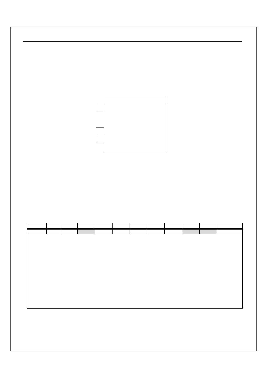
FIGURE 9-1: Port-A Configuration Function Block Diagram
VCC
PORT
DATA
REGISTER
( PDR )
PULL-UP
PMOS
PULL-UP
RD_INPUT
DATA INPUT
PORT
CONTROL
REGISTER
( PCR )
Address Name R/W
Bit 7
Bit 6
Bit 5
Bit 4
Bit 3
Bit 2
Bit 1
Bit 0
Default
$00F PMCR R/W PULL PDBN
INTEG -
-
-
PSG0
PSGB
100 - - -00
Bit 7: PULL : Enable all pull-up function bit
1 = Enable pull-up function
0 = Disable pull-up function
Bit 6: PDBN : Enable Port-A interrupt debounce bit*
1 = Debounce for Port-A interrupt
0 = No debounce for Port-A interrupt
Bit 5: INTEG : INTX interrupt edge select bit**
1 = Rising edge
0 = falling edge
* No de-bounce function when Port-A disable interrupt.
** INTX interrupt no de-bounce function.
TABLE 9-9: PORT CONDITION CONTROL REGISTER (PMCR)
ST2006
Ver 1.21
14/38
2003/
7/4
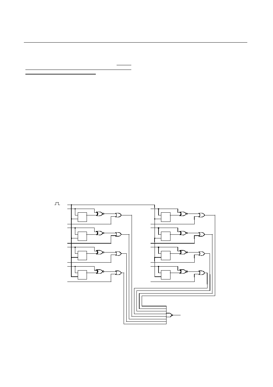
9.2.3 Port-A
interrupt
Port-A, a programmable I/O, can be used as a port interrupt
when it is in the input mode. Any edge transition of the
Port-A input pin will generate an interrupt request. The last
state of Port-A must be kept before I/O transition and this
can be accomplished by reading Port-A.
When programmer enables INTX and PT interrupts, PA0
trigger will occur. INTX and PT interrupts will therefore
happen sequentially. Please refer to the FIGURE 1-2: .
Operating Port-A interrupt step by step :
1. Set input mode.
2. Read Port-A.
3. Clear interrupt request flag (IRPT).
4. Set interrupt enable flag (IEPT).
5. Clear CPU interrupt disable flag (I).
6. Read Port-A before `RTI' instruction in
INT-Subroutine.
Example :
.
.
.
STZ
PCA
LDA #$FF
LDA
PA
RMB4 <IREQ
SMB4 <IENA
CLI
.
.
INT-SUBROUTINE
.
.
LDA
PA
RTI
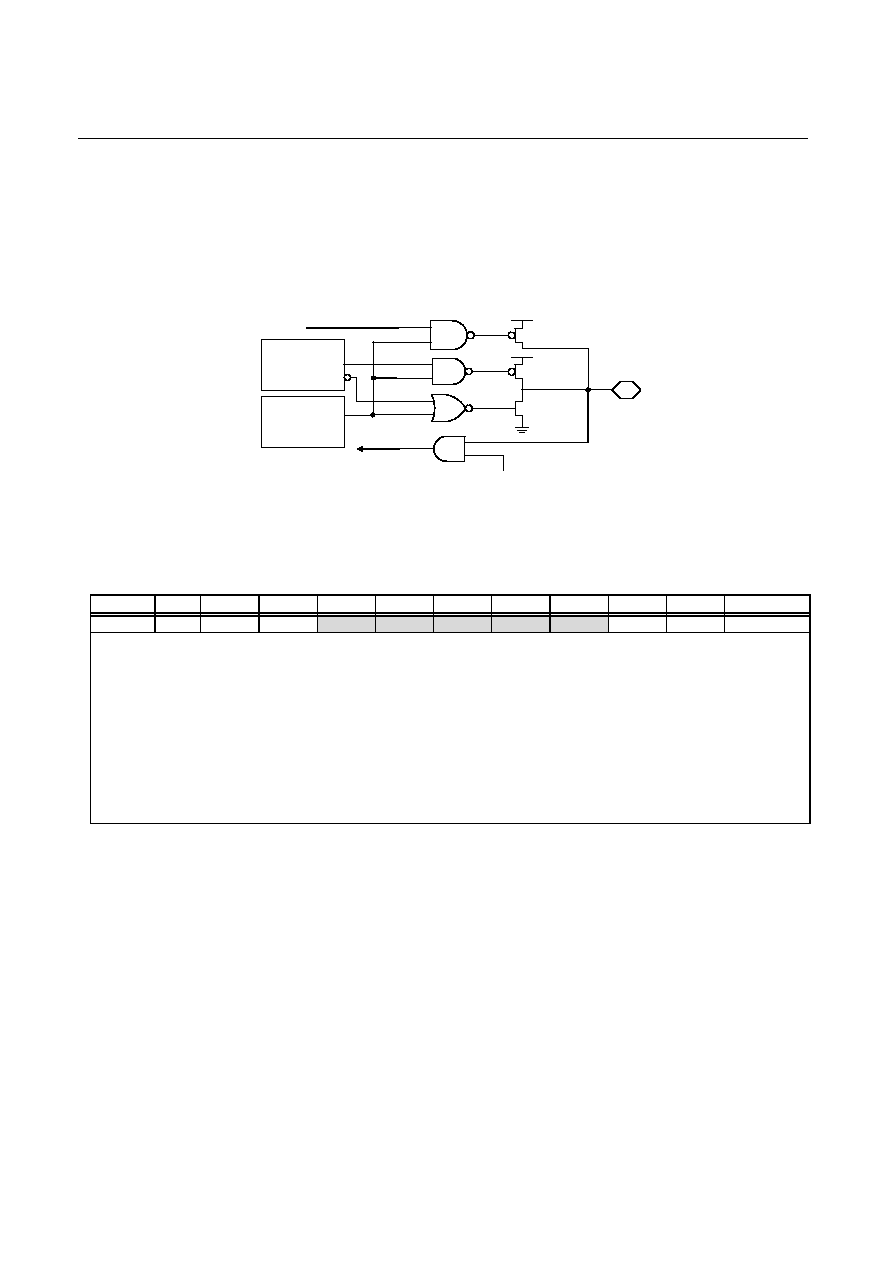
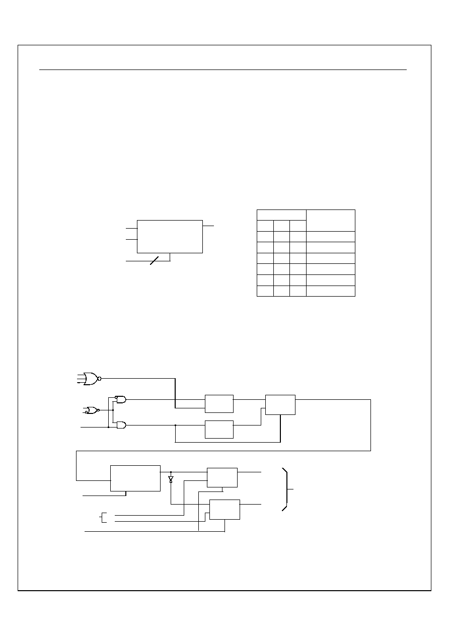
FIGURE 9-2: Port Interrupt Logic Diagram
NAND8
OR2
OR2
OR2
OR2
OR2
OR2
OR2
OR2
DFF
CK
D
Q
DFF
CK
D
Q
DFF
CK
D
Q
DFF
CK
D
Q
DFF
CK
D
Q
DFF
CK
D
Q
DFF
CK
D
Q
DFF
CK
D
Q
XNOR2
XNOR2
XNOR2
XNOR2
XNOR2
XNOR2
XNOR2
XNOR2
RDPA
PA[0]
PA[4]
PCA[0]
PCA[4]
PA[1]
PA[5]
PCA[1]
PCA[5]
PA[2]
PA[6]
PCA[2]
PCA[6]
PA[3]
PA[7]
PCA[3]
PCA[7]
PTIR
High Level Interrupt
ST2006
Ver 1.21
15/38
2003/
7/4
9.2.3.1
Port-A interrupt debounce
ST2006 has hardware debounce option for Port-A interrupt.
The debounce will be enabled with "1" and disable with "0"
for PDBN. The debounce will active when Port-A transition
occurs, PDBN enable and OSCX enable.
The debounce time is OSCX x 512 cycles(about 16 ms).
Refer to 0 .
Address Name R/W
Bit 7
Bit 6
Bit 5
Bit 4
Bit 3
Bit 2
Bit 1
Bit 0
Default
$00F PMCR R/W
PULL PDBN INTEG
-
-
-
PSG0
PSGB
100 - - -00
Bit 6: PDBN : Enable Port-A interrupt debounce bit
1 = Debounce for Port-A interrupt
0 = No debounce for Port-A interrupt
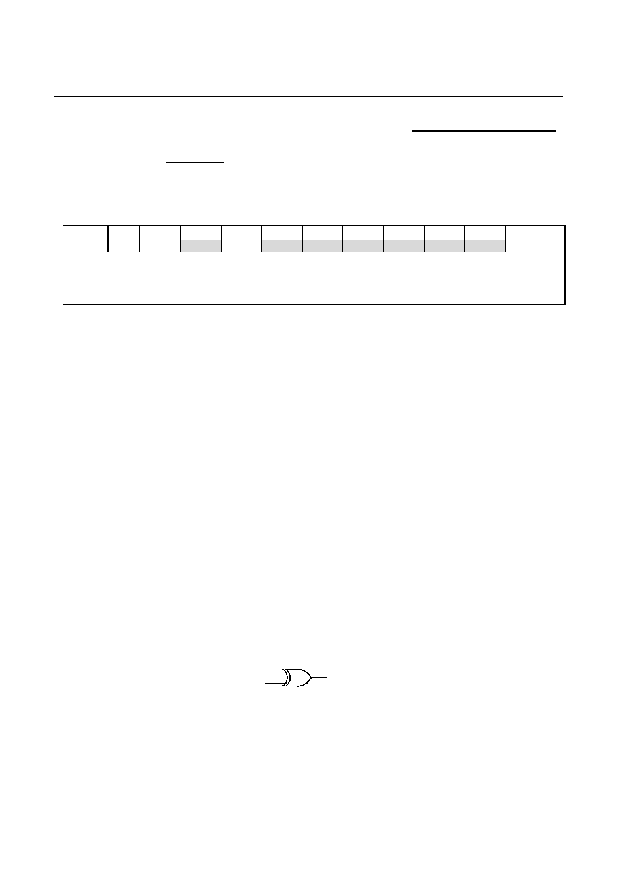
9.2.4 PA0/INTX
PA0 can be used as an external interrupt input(INTX).
Falling or Rising edge is controlled by INTEG(PMCR[5]) and
the external interrupt is set up with "0" for falling edge and "1"
for rising edge.
When programmer enables INTX and PT interrupts, PA0
trigger will occur. Both INTX and PT interrupts will happen
sequentially. Please refer to the operating steps.
Operating INTX interrupt step by step :
1.
Set PA0 pin into input mode. (PCA[0])
2.
Select edge level. (INTEG)
3.
Clear INTX interrupt request flag. (IRX)
4.
Set INTX interrupt enable bits. (IEX)
5.
Clear CPU interrupt mask flag (I).
Example :
.
.
.
RMB0 <PCA
;Set
input
mode.
SMB5 <PMCR
;Rising
edge.
RMB0 <IREQ
;Clear
IRQ
flag.
SMB0 <IENA
;Enable
INTX
interrupt.
CLI
.
.
.
FIGURE 9-3: INTX Logic Diagram
PMCR[5]
PA 0/INTX
Falling Edge Interrupt
TABLE 9-10: PORT CONDITION CONTROL REGISTER (PMCR)
ST2006
Ver 1.21
16/38
2003/
7/4
9.3 PORT-B
Port -B is a bit programmable bi-direction I/O port, which is
controlled by PCB register. It also provides user with bit-
programmable pull-up MOS and sound output port
separately.
Address Name R/W
Bit 7
Bit 6
Bit 5
Bit 4
Bit 3
Bit 2
Bit 1
Bit 0
Default
$001 PB
R/W
-
-
-
-
PB[3]
PB[2]
PB[1]
PB[0]
- - - - 1111
$009 PCB R/W
-
-
-
-
PCB[3] PCB[2] PCB[1] PCB[0] - - - - 0000
$00F PMCR R/W PULL PDBN
INTEG
-
-
-
PSG0
PSGB
100 - - -00
1.1.1 PORT-B
I/O
control
Direction of Port-B is controlled by PCB. Every bit of
PCB[3-0] is mapped into the I/O direction of PB[3-0]
correspondingly, with "1" for output mode, and "0" for input
mode.
Address Name R/W
Bit 7
Bit 6
Bit 5
Bit 4
Bit 3
Bit 2
Bit 1
Bit 0
Default
$009 PCB R/W
-
-
-
-
PCB[3] PCB[2] PCB[1] PCB[0] - - - - 0000
Bit 1~0: PCB[3~0] : Port-B directional bits
1 = Output mode
0 = Input mode
TABLE 9-11: SUMMARY FOR PORT-B REGISTERS
TABLE 9-12: PORT-B CONTROL REGISTER (PCB)
ST2006
Ver 1.21
17/38
2003/
7/4
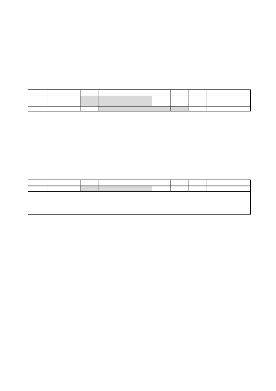
9.3.1 PORT-B
PULL-UP
OPTION
This port contains pull-up MOS transistors which is
controlled by software and can be enabled or disabled with
"1" or with "0" accordingly in data bit of the port data register
(PB) when an I/O is used as an input. The PULL control bit of
PMCR also controls the ON/OFF of all the pull-up MOS
simultaneously. Please refer to the FIGURE 1-4: .
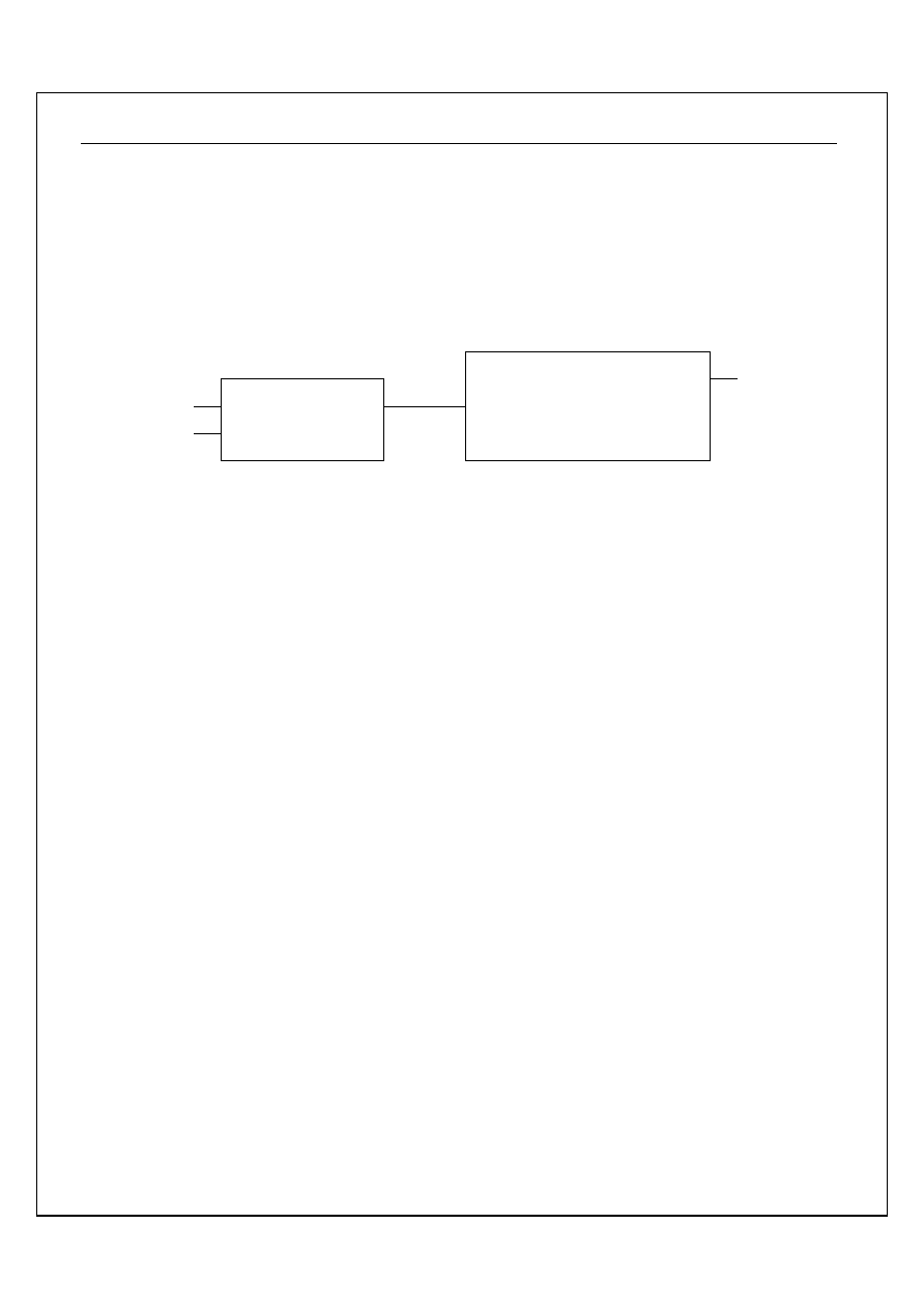
FIGURE 1-4: Port-B Configuration Function Block Diagram
VCC
PORT
DATA
REGISTER
( PDR )
PULL-UP
PMOS
PULL-UP
RD_INPUT
DATA INPUT
PORT
CONTROL
REGISTER
( PCR )
Address Name R/W
Bit 7
Bit 6
Bit 5
Bit 4
Bit 3
Bit 2
Bit 1
Bit 0
Default
$00F PMCR R/W PULL PDBN
INTEG
-
-
-
PSG0
PSGB
100 - - -00
Bit 7: PULL : Enable all pull-up functions bit
1 = Enable pull-up function
0 = Disable pull-up function
Bit 1: PSGO : PSG output enable bit
1 = PB3 is PSG data output pin if PB3 is set in output mode
0 = PB3 is normal I/O pin
Bit 0: PSGB : PSG inverse signal output enable bit
1 = PB2 is PSG inverse data output pin if PB2 is set in output mode
0 = PB2 is normal I/O pin
TABLE 9-13: PORT CONDITION CONTROL REGISTER (PMCR)
ST2006
Ver 1.21
18/38
2003/
7/4
9.4 SEGMENT-PORT
The SEG0~SEG3 and SEG4~SEG7 can be used as LCD
drivers or output ports. In output port mode, programmer
must write $FF($00) into LCD RAM in order to output
HIGH(LOW). The assignments of SEGOX will be decided by
Bit 3~2 of LCTL[3~2]. Please refer to 9.4TABLE 9-14: .
Address Name R/W
Bit 7
Bit 6
Bit 5
Bit 4
Bit 3
Bit 2
Bit 1
Bit 0
Default
$03A LCTL W
LPWR BLANK
-
- SEGO1
SEGO0 -
DUTY
00- - 00-0
Bit 3: SEGO1 : Segment output selection bit
1 = SEG0-SEG3 used as output pins
0 = SEG0-SEG3 used as LCD segment pins
Bit 2: SEGO0 : Segment output selection bit
1 = SEG4-SEG7 used as output pins
0 = SEG4-SEG7 used as LCD segment pins
Address
Name
R/W Bit 7
Bit 6
Bit 5
Bit 4
Bit 3
Bit 2
Bit 1
Bit 0
Default
$200
SEGMENT OUT 0 W
SEGMENT-0 OUTPUT BIT
???? ????
$201
SEGMENT OUT 1 W
SEGMENT-1 OUTPUT BIT
???? ????
$202
SEGMENT OUT 2 W
SEGMENT-2 OUTPUT BIT
???? ????
$203
SEGMENT OUT 3 W
SEGMENT-3 OUTPUT BIT
???? ????
$204
SEGMENT OUT 4 W
SEGMENT-4 OUTPUT BIT
???? ????
$205
SEGMENT OUT 5 W
SEGMENT-5 OUTPUT BIT
???? ????
$206
SEGMENT OUT 6 W
SEGMENT-6 OUTPUT BIT
???? ????
$207
SEGMENT OUT 7 W
SEGMENT-7 OUTPUT BIT
???? ????
In the output port mode, programmer must write $FF($00) into LCD RAM to output HIGH(LOW).
TABLE 9-14: LCD CONTROL REGISTER (LCTL)
TABLE 9-15: SEGMENT OUT REGISTER
ST2006
Ver 1.21
19/38
2003/
7/4
1
1
0
0
.
.
O
O
s
s
c
c
i
i
l
l
l
l
a
a
t
t
o
o
r
r
ST2006 is with dual-clock system. Programmer can choose
between OSC(RC) and OSCX(32.768k), or both as clock
source through program. The system clock(SYSCK) also
can be switched between OSC and OSCX. The OSC will be
switch with "0" and OSCX will be switch with "1" for XSEL.
Whenever system clock be switch, the warm-up cycles are
occur at the same time. That is confirm SYSCK really
switched when read XSEL bit. LCD driver, Timer1, Base
Timer and PSG can utilize these two clock sources as well.
Address Name R/W
Bit 7
Bit 6
Bit 5
Bit 4
Bit 3
Bit 2
Bit 1
Bit 0
Default
$030 SYS R/W XSEL OSTP XSTP XBAK WSKP WAIT
-
-
0000 00- -
Bit 7: XSEL : System clock select(write) / confirm(read) bit
1 = OSCX
0 = OSC
Bit 6: OSTP : OSC stop control bit
1 = Disable OSC
0 = Enable OSC
Bit 5: XSTP : OSCX stop control bit
1 = Disable OSCX
0 = Enable OSCX
Bit 4: XBAK : OSCX driver heavy load bit
1 = OSCX normal load
0 = OSCX heavy load
Bit 3: WSKP : System warm-up control bit
1 = Warm-up to 16 oscillation cycles
0 = Warm-up to 256 oscillation cycles
Bit 2: WAIT : WAI-0 / WAI-1mode select bit (Refer to POWER DOWN MODE)
1 = WAI instruction causes the chip to enter WAI-1 mode
0 = WAI instruction causes the chip to enter WAI-0 mode
Note:
1. The XSEL(SYS[7]) bit will show which real working mode is when it is read.
FIGURE 9-5: System Clock Diagram
2
IN
OUT
MUX2
IN0
IN1
OUTPUT
SEL
OSC
SYSCK
OSCX
XSEL
Frequency divided by 2
TABLE10-16: SYSTEM CONTROL REGISTER (SYS)
ST2006
Ver 1.21
20/38
2003/
7/4
1
1
1
1
.
.
T
T
I
I
M
M
E
E
R
R
/
/
E
E
V
V
E
E
N
N
T
T
C
C
O
O
U
U
N
N
T
T
E
E
R
R
The ST2006 has two timers: Base timer/Timer1, and two
prescalers (PRES and PREW). There are two clock sources
for PRES and one clock source(OSCX) for PREW. Please
refer to the following table:
SENT Clock
source(TCLK) MODE
1 INTX
Event
counter
0 SYSCK Timer
Address Name R/W
Bit 7
Bit 6
Bit 5
Bit 4
Bit 3
Bit 2
Bit 1
Bit 0
Default
$021 BTM
W
-
-
-
- BTM[3]
BTM[1] BTM[0]
- - - - 0-00
R
PRS[7] PRS[6] PRS[5] PRS[4] PRS[3] PRS[2] PRS[1] PRS[0] 0000
0000
$023 PRS
W SRES SENA SENT
-
-
-
-
-
000 - - - - -
$026 T1M R/W
-
-
- T1M[4]
T1M[3]
T1M[1] T1M[0]
- - -0 0-00
$027 T1C
R/W T1C[7] T1C[6] T1C[5] T1C[4] T1C[3] T1C[2] T1C[1] T1C[0] 0000
0000
$030 SYS R/W XSEL OSTP XSTP XBAK
WSKP WAIT
-
-
0000 00- -
$03C IREQ R/W
-
- IRBT
IRPT IRT1 -
-
IRX
- - 00 0-00
$03E IENA R/W
-
- IEBT
IEPT IET1 -
-
IEX
- - 00 0-00
SYSCK
INTX
SENT
O
SEL
MUX
SRES-PULSE
SENA
CK
ENABLE
CLEAR
OUTPUT
TCLK
PREW
OUTPUT
OSCX/256
OSCX/64
OSCX/16
OSCX/4
CK
RESET
OSCX
RESET
IN0
IN1
TCLK/256
TCLK/32
TCLK/8
TCLK/2
PRES
BASE TIMER
TIMER 1
OSCX/128
OSCX/32
FIGURE 9-6: Prescaler for Timers
TABLE11-17: CLOCK SOURCE (TCLK) FOR PRES
TABLE11-18: SUMMARY FOR TIMER REGISTERS
ST2006
Ver 1.21
21/38
2003/
7/4
11.1 PRES
The prescaler PRES is an 8-bits counter as shown in Figure
11-6. Which provides four clock sources for base timer and
timer1, and it is controlled by register PRS. The instruction
read toward PRS will bring out the content of PRES and the
instruction write toward PRS will reset, enable or select clock
sources for PRES.
When user set external interrupt as the input of PRES for
event counter, combining PRES and Timer1 will get a
16bit-event counter.
Address Name R/W
Bit 7
Bit 6
Bit 5
Bit 4
Bit 3
Bit 2
Bit 1
Bit 0
Default
R
PRS[7] PRS[6] PRS[5] PRS[4] PRS[3] PRS[2] PRS[1] PRS[0] 0000
0000
$023 PRS
W SRES SENA SENT
-
-
-
-
-
000 - - - - -
READ
Bit 7~0: PRS[7~0] : 1's complement of PRES counter
WRITE
Bit 7: SRES : Prescaler Reset bit
Write "1" to reset the prescaler (PRS[7~0])
Bit 6: SENA : Prescaler enable bit
0 = Disable prescaler counting
1 = Enable prescaler counting
Bit 5: SENT : Clock source(TCLK) selection for prescaller PRES
0 = Clock source from system clock "SYSCK"
1 = Clock source from external events "INTX"
11.2 PREW
The prescaler PREW is an 8-bits counter as shown in Figure
11-6. PREW provides four clock source for base timer and
timer1. It stops counting only if OSCX stops or hardware
reset occurs.
TABLE 11-19: PRESCALER CONTROL REGISTER (PRS)
ST2006
Ver 1.21
22/38
2003/
7/4
11.3 Base timer
11.3.1 Structure of Base Timer
Base timer is an 8-bit up counting timer. When it overflows
from $FF to $00, a timer interrupt request IRBT will be
generated. Please refer to FIGURE 1-2: :
FIGURE 1-2: Structure of Base Timer
IN0
IN1
IN2
IN3
SEL
PRES
BTM[1~0]
MUX4-1
PREW
IN0
IN1
IN2
IN3
SEL
BTM[1~0]
BTM[3]
IN0
IN1
SEL
MUX
8 Bit - UP Counter
CLOCK
IRBT
MUX 4-1
OSCX/256
OSCX/64
OSCX/16
OSCX/4
TCLK/256
TCLK/32
TCLK/8
TCLK/2
OUT
OUT
OUT
11.3.2 Clock source control for Base Timer
Several clock sources can be selected for Base Timer.
Please refer to the following table:
*
SENA BTM[3] BTM[1] BTM[0] Base
Timer
source
clock
0 0 X
X STOP
1 0 0 0
TCLK
/
256
1 0 0 1
TCLK
/
32
1 0 1 0
TCLK
/
8
1
0
1
1
TCLK / 2
X 1 0 0
OSCX
/
256
X 1 0 1
OSCX
/
64
X 1 1 0
OSCX
/
16
X 1 1 1
OSCX
/
4
* TCLK will stop when an `0' is written to SENA(PRS[6]).
TABLE11-20: CLOCK SOURCE FOR BASE TIMER
ST2006
Ver 1.21
23/38
2003/
7/4
11.4 Timer 1
11.4.1 General function
The Timer1 is an 8-bit up counter. It can be used as a timer
or an event counter. T1C($27) is a real time read/write
counter. When an overflow from $FF to $00, a timer interrupt
request IRT1 will be generated. Timer1 will stop counting
when system clock stops. Please refer to FIGURE 1-3: .
FIGURE 1-3: Timer1 Structure Diagram
IN0
IN1
IN2
IN3
SEL
PRES
T1M[1~0]
MUX4-1
PREW
IN0
IN1
IN2
IN3
SEL
T1M[1~0]
MUX
8 Bit - UP Counter
CLOCK
IRT1
MUX 4-1
OSCX/256
OSCX/128
OSCX/64
OSCX/32
TCLK/256
TCLK/32
TCLK/8
TCLK/2
OUT
OUT
IN0
IN1
OUT
SEL
D
CK
Q
D Flip-Flop
SYSCK
MUX
T1M[3]
Auto Reload
T1M[4]
Address Name R/W
Bit 7
Bit 6
Bit 5
Bit 4
Bit 3
Bit 2
Bit 1
Bit 0
Default
$027 T1C
R/W T1C[7] T1C[6] T1C[5] T1C[4] T1C[3] T1C[2] T1C[1] T1C[0] 0000
0000
11.4.1.1
Bit 7-0: T1C[7-0] : Timer1 up counter register
TABLE 11-21: TIMER1 COUNTING REGISTER (T1C)
ST2006
Ver 1.21
24/38
2003/
7/4
11.4.2 Clock source control for Timer1
Several clock source can be chosen from for Timer1. It's
very important that Timer1 can keep counting as long as
SYSCK stays active. Refer to the following table:
*
SENA T1M[4] T1M[3] T1M[1] T1M[0] Clock
source
Auto-Reload
0
X 0 X
X STOP
-
1 0 0 0 0
TCLK
/
256 No
1 0 0 0 1
TCLK
/
32 No
1 0 0 1 0
TCLK
/
8 No
1 0 0 1 1
TCLK
/
2 No
X 0 1 0 0
OSCX
/
256
No
X 0 1 0 1
OSCX
/
128
No
X 0 1 1 0
OSCX
/
64 No
X 0 1 1 1
OSCX
/
32 No
1 1 0 0 0
TCLK
/
256
Yes
1 1 0 0 1
TCLK
/
32 Yes
1 1 0 1 0
TCLK
/
8 Yes
1 1 0 1 1
TCLK
/
2 Yes
X 1 1 0 0
OSCX
/
256
Yes
X 1 1 0 1
OSCX
/
128
Yes
X 1 1 1 0
OSCX
/
64 Yes
X 1 1 1 1
OSCX
/
32 Yes
* TCLK would stop when SENA is set to 0.
TABLE 11-22: CLOCK SOURCE FOR TIMER1
ST2006
Ver 1.21
25/38
2003/
7/4
1
1
2
2
.
.
P
P
S
S
G
G
12.1 General Function
The built-in Programmable Sound Generator (PSG) is
controlled by registers directly. Its flexibility through setting
several parameters to registers makes it useful in many
applications, such as music synthesis, sound effects
generation, audible alarms and tone generation. PSG will
finish the reset when user needs to create sound effect. The
structure of PSG is shown in FIGURE 1-5: and its clock
sources are shown in FIGURE 1-4: There are two sound
types for PSG; tone and noise.
FIGURE 9-4: Clock Source for PSG
SYSCK
OSCX
PSGC[6~4]
IN0
IN1
Output
Select
PSG Selector
PSGCK
PSGC
SYSCK/2
PSGCK
SYSCK/4
SYSCK/8
SYSCK/16
SYSCK
OSCX
B6 B5 B4
0
0
0
X
X
0
1
1
1
1
1
1
1
0
1
0
0
0
FIGURE 9-5: Program Sound Generator
Enable Output
Enable
LOAD
Output
MUX2
IN0
IN1
OUTPUT
SEL
MUX2
IN0
IN1
OUTPUT
SEL
MUX2
IN0
IN1
OUTPUT
SEL
MIXER
CH1
Output
Vol_CH1
DACE
C1TEN
C1Tone
C1out
DACE
PSGC[2]
C1NEN
C1Noise
PSGC[3]
PSGOUT
C1out
VOL[1~0]
PSGOUTB
BD
BDB
DACE
To Port B
From DAC Generator
Channel 1 Tone
Channel 1 Noise
Preload Data Before First Count
ST2006
Ver 1.21
26/38
2003/
7/4
Address Name R/W
Bit 7
Bit 6
Bit 5
Bit 4
Bit 3
Bit 2
Bit 1
Bit 0
Default
$00F PMCR R/W
PULL
PDBN
INTEG
-
-
-
PSGO
PSGB
100 - - -00
$012 PSGL W PSG[7] PSG[6] PSG[5] PSG[4] PSG[3] PSG[2] PSG[1] PSG[0] 0000
0000
$013 PSGH W
-
-
-
-
PSG[11] PSG[10] PSG[9] PSG[8] - - - - 0000
$016 PSGC W
-
PCK[2] PCK[1] PCK[0] PRBS C1EN
-
-
- 000 00--
$017 VOL
W VOL[1]
VOL[0] -
-
-
-
-
-
00 - - - - - -
Address Name R/W
Bit 7
Bit 6
Bit 5
Bit 4
Bit 3
Bit 2
Bit 1
Bit 0
Default
$00F PMCR R/W
PULL
PDBN
INTEG
-
-
-
PSGO
PSGB
100 - - -00
Bit 1: PSGO : PSG output enable bit
1 = PSG data output pin if PB3 is set in output mode
0 = PB3 is normal I/O pin
Bit 0: PSGB : PSG inverse signal output enable bit
1 = PB2 is PSG inverse data output pin if PB2 is set in output mode
0 = PB2 is normal I/O pin
Address Name R/W
Bit 7
Bit 6
Bit 5
Bit 4
Bit 3
Bit 2
Bit 1
Bit 0
Default
$017 VOL
W VOL[1]
VOL[0] -
-
-
-
-
-
00 - - - - - -
Bit 7~6: VOL[1~0] : PSG volume control bit
00 = No sound output
01 = 1/4 volume (PSGCK must >= 128K Hz)
10 = 1/2 volume (PSGCK must >= 64K Hz)
11 = Maximum volume (PSGCK must >= 32K Hz)
TABLE 12-23: SUMMARY FOR PSG REGISTERS
TABLE 12-24: CONTROL REGISTER FOR PSG OUTPUT (PMCR)
TABLE 12-25: CONTROL REGISTER FOR PSG VOLUME (VOL)
ST2006
Ver 1.21
27/38
2003/
7/4
12.2 Tone Generator
The tone frequency is decided by PSGCK and 12-bit
programmable divider (PSG[11~0]) Please refer to FIGURE
1-3:
FIGURE 1-3: PSG Tone Counter
12 Bit Auto-reload Up Counter
Tone out
OUTPUT
PSG[11~8]
PSG[7~0]
LOAD
C1EN
PSGCK
C1[11~8]
C1[7~0]
Latch
Enable
Tone Frequency = PSGCK/(1000H-PSG[11~0])/2
CLOCK
12.3 PSG Tone programming
To program tone generator, PSGO (PMCR[1]) or PSGB
(PMCR[ 0]) should be set to "1" for PB1 or PB0 in order to be
in the PSG output mode. Writing to C1EN will enable tone
generator when PSG is in tone function. Noise or tone
function is selected by PRBS.
Address Name R/W
Bit 7
Bit 6
Bit 5
Bit 4
Bit 3
Bit 2
Bit 1
Bit 0
Default
$016 PSGC W
-
PCK[2] PCK[1] PCK[0] PRBS C1EN
-
-
- 000 00--
Bit 2: C1EN : PSG (Tone or Noise) enable bit
1 = PSG (Tone or Noise) enable
0 = PSG (Tone or Noise) disable
Bit 3: PRBS : Tone or Noise generator selection bit
1 = Noise generator
0 = Tone generator
Bit 6~4: PCK[2~0] : clock source PSGK selection for PSG
000 = SYSCK / 2
X01 = SYSCK / 4
X10 = SYSCK / 8
011 = SYSCK / 16
100 = SYSCK
111 = OSCX
TABLE 12-26: PSG CONTROL REGISTER (PSGC)
ST2006
Ver 1.21
28/38
2003/
7/4
12.4 Noise Generator Control
Noise generator is shown in FIGURE 1-4: , which base
frequency is controlled by PSGL[5~0].
FIGURE 1-4: Noise Generator Diagram
PSG[5~0]
PSGCK
Noise Prescaler
C1N[5~0]
CLOCK
OUTPUT
NCK
CLOCK
OUTPUT
16-Stage White Noise Generator
Noise out
NCK Frequency = PSGCK/(40H-PSG[5~0])
12.5 PSG Noise programming
To program noise generator, PSGO (PMCR[1]) or PSGB
(PMCR[0]) should be set to "1" for PB3 or PB2 in order to be
in PSG output. Writing a "1" to C1EN will enable noise
generator when PSG is in noise mode.
ST2006
Ver 1.21
29/38
2003/
7/4
1
1
3
3
.
.
L
L
C
C
D
D
The ST2006 can drive up to 128 dots of LCD panel directly.
The LCD driver can control by 1/3 duty (96 dots) and 1/4
duty (128 dots). LCD block include display RAM ($200~
$21F) for storing the display data, 32-segment output pins
(SEG0~SEG31), 4-common output pins (COM0~COM3).
All LCD RAM are random after power on reset.
FIGURE 13-2: Clock source of LCD
SYSCK
INTX
SENT
O
SEL
MUX
SRES-PULSE
SENA
CK
ENABLE
CLEAR
OUTPUT
TCLK
IN0
IN1
TCLK/64
TCLK/32
TCLK/16
TCLK/8
PRES
MUX4-1
IN0
IN3
IN2
IN1
SEL
OUT
LCK[1~0]
IN0
IN1
OSCX
SEL
LCK[2]
OUT
IN
OUT
:
64
LCD clock
ST2006
Ver 1.21
30/38
2003/
7/4
13.2 LCD driver 1/4 duty output
COM0
COM1
COM2
COM3
SEGx
SEGx
All Off
All On
V0
V1
V2
V3
1/4 duty , 1/3 bias LCD signal
V0
V1
V2
V3
V0
V1
V2
V3
V0
V1
V2
V3
Phase1
Phase2
V0
V1
V2
V3
V0
V1
V2
V3
COM3
COM2
COM1
COM0
SEGx+1
SEGx
Example
SEGx
SEGx
V0
V1
V2
V3
V0
V1
V2
V3
Phase1
Phase2
ST2006
Ver 1.21
31/38
2003/
7/4
13.3 LCD control register
TABLE 13-27: LCD CONTROL REGISTER (LCTL)
Address Name R/W
Bit 7
Bit 6
Bit 5
Bit 4
Bit 3
Bit 2
Bit 1
Bit 0
Default
$020 LCK
W
-
-
-
-
-
LCK[2] LCK[1] LCK[0]
- - - - -100
$023 PRS
W SRES SENA SENT
-
-
-
-
-
000 - - - - -
$03A LCTL W LPWR
BLANK -
- SEGO1
SEGO0 -
DUTY
00- - 00-0
Address Name R/W
Bit 7
Bit 6
Bit 5
Bit 4
Bit 3
Bit 2
Bit 1
Bit 0
Default
$020 LCK
W
-
-
-
-
-
LCK[2] LCK[1] LCK[0]
- - - - -100
Bit 2~0: LCK[2~0] : LCD clock source
000 = TCLK / 4096 ( LCD frame clock = TCLK / 32768 ) *
001 = TCLK / 2048 ( LCD frame clock = TCLK / 16384 ) *
010 = TCLK / 1024 ( LCD frame clock = TCLK / 8192 ) *
011 = TCLK / 512 ( LCD frame clock = TCLK / 4096 ) *
1XX = OSCX / 64 ( LCD frame clock = 64 )
* SENA must switch "1". ( refer to FIGURE 13-1 )
Address Name R/W
Bit 7
Bit 6
Bit 5
Bit 4
Bit 3
Bit 2
Bit 1
Bit 0
Default
$03A LCTL W LPWR
BLANK -
- SEGO1
SEGO0 -
DUTY
00- - 00-0
Bit 7: LPWR : LCD power ON/OFF bit
1 = LCD power OFF
0 = LCD power ON
Bit 6: BLANK : LCD display ON/OFF bit
1 = Disable LCD display (Common line is still scanning)
0 = Enable LCD display
Bit 3: SEGO1 : mode control for LCD segment output
1 = SEG3~SEG0 will be general purpose output pin only
0 = SEG3~SEG0 output is used as LCD segment driver.
Bit 2: SEGO0 : mode control for LCD segment output
1 = SEG7~SEG4 will be general purpose output pin only
0 = SEG7~SEG4 output is used as LCD segment driver.
Bit 0: DUTY : LCD duty control bit
1 = 1/3 duty (1/2 bias)
0 = 1/4 duty (1/3 bias)
TABLE 13-28: LCD FREQUENCY REGISTER (LCK)
TABLE 13-29: LCD CONTROL REGISTER (LCTL)
ST2006
Ver 1.21
32/38
2003/
7/4
13.4 LCD RAM MAPPING
The LCD RAM map is shown as the following:
SEGO ADDRESS COM0 COM1 COM2 COM3
0
200H
Bit 0
Bit 1
Bit 2
Bit 3
1
201H
Bit 0
Bit 1
Bit 2
Bit 3
2
202H
Bit 0
Bit 1
Bit 2
Bit 3
3
203H
Bit 0
Bit 1
Bit 2
Bit 3
4
204H
Bit 0
Bit 1
Bit 2
Bit 3
5
205H
Bit 0
Bit 1
Bit 2
Bit 3
6
206H
Bit 0
Bit 1
Bit 2
Bit 3
7
207H
Bit 0
Bit 1
Bit 2
Bit 3
8
208H
Bit 0
Bit 1
Bit 2
Bit 3
9
209H
Bit 0
Bit 1
Bit 2
Bit 3
10
20AH
Bit 0
Bit 1
Bit 2
Bit 3
11
20BH
Bit 0
Bit 1
Bit 2
Bit 3
12
20CH
Bit 0
Bit 1
Bit 2
Bit 3
13
20DH
Bit 0
Bit 1
Bit 2
Bit 3
14
20EH
Bit 0
Bit 1
Bit 2
Bit 3
15
20FH
Bit 0
Bit 1
Bit 2
Bit 3
16
210H
Bit 0
Bit 1
Bit 2
Bit 3
17
211H
Bit 0
Bit 1
Bit 2
Bit 3
18
212H
Bit 0
Bit 1
Bit 2
Bit 3
19
213H
Bit 0
Bit 1
Bit 2
Bit 3
20
214H
Bit 0
Bit 1
Bit 2
Bit 3
21
215H
Bit 0
Bit 1
Bit 2
Bit 3
22
216H
Bit 0
Bit 1
Bit 2
Bit 3
23
217H
Bit 0
Bit 1
Bit 2
Bit 3
24
218H
Bit 0
Bit 1
Bit 2
Bit 3
25
219H
Bit 0
Bit 1
Bit 2
Bit 3
26
21AH
Bit 0
Bit 1
Bit 2
Bit 3
27
21BH
Bit 0
Bit 1
Bit 2
Bit 3
28
21CH
Bit 0
Bit 1
Bit 2
Bit 3
29
21DH
Bit 0
Bit 1
Bit 2
Bit 3
30
21EH
Bit 0
Bit 1
Bit 2
Bit 3
31
21FH
Bit 0
Bit 1
Bit 2
Bit 3
Note:
1. The LCD RAM address is allocated at page 2 of memory map. Only bit0 ~ bit2 is useful when it is 1/3 duty
mode.
2. The LCD RAM can be write & read as like general purpose RAM.
TABLE 13-30: LCD RAM MAPPING
ST2006
Ver 1.21
33/38
2003/
7/4
1
1
4
4
.
.
P
P
o
o
w
w
e
e
r
r
D
D
o
o
w
w
n
n
M
M
o
o
d
d
e
e
The ST2006 has three power down modes: WAI-0, WAI-1
and STP. The instruction WAI will enable mode WAI-0 or
WAI-1, which are controlled by WAIT(SYS[2]). The
instruction WAI (WAI-0 and WAI-1 modes) can be wake-up
by interrupt. However, the instruction of STP can only be
wake-up by hardware reset.
14.1 WAI-0 Mode:
When WAIT is cleared, WAI instruction lets MCU enter
WAI-0 mode. In the mean time, oscillator circuit is be active
and interrupts, timer/counter, and PSG will all be working.
Under such circumstance, CPU stops and the related
instruction execution will stop. All registers, RAM, and I/O
pins will retain their states before the MCU enter standby
mode. WAI-0 mode can be wake-up by reset or interrupt
request. If user disable interrupt(CPU register I='1'), MCU
will still be wake-up but not go into the interrupt service
routine. If interrupt is enabled(CPU register I='0'), the
corresponding interrupt vector will be fetched and interrupt
service routines will executed.
The sample program is showed as followed:
LDA #$00
STA SYS
WAI
; WAI 0 mode
14.2 WAI-1 Mode:
When WAIT is set, WAI instruction let MCU to enter WAI-1
mode. In this mode, the CPU will stop, but PSG,
timer/counter won't stop if the clock source is from OSCX.
The wake-up procedure is the same as the one for WAI-0.
But the warm-up cycles are occur when WAI-1 wake-up.
The sample program is shown as the following:
LDA #$04
STA SYS
WAI
; WAI 1 mode
14.3 STP Mode:
STP instruction will force MCU to enter stop mode. In this
mode, MCU stops, but PSG, timer/counter won't stop if the
clock source is from OSCX. In power-down mode, MCU only
be wake-up by hardware reset, and the warm-up cycles are
occur at the same time.
The sample program is showed as the following:
.
.
STP
.
.
(SYSCK source from OSC)
Mode
Timer1 SYSCK OSC OSCX
Base
Timer
RAM REG. LCD I/O Wake-up
condition
WAI-0
Retain
Reset, Any interrupt
WAI-1 Stop
Stop
Stop
Retain
Reset, Any interrupt
STP
Stop Stop Stop
Retain
Reset
(SYSCK source from OSCX)
Mode
Timer1 SYSCK OSC OSCX
Base
Timer
RAM REG. LCD I/O Wake-up
condition
WAI-0
Retain
Reset, Any interrupt
WAI-1 Stop
Stop Retain
Reset, Any interrupt
STP
Stop
Stop Retain
Reset
TABLE 14-31: STATUS UNDER POWER DOWN MODE
ST2006
Ver 1.21
34/38
2003/
7/4
1
1
5
5
.
.
E
E
l
l
e
e
c
c
t
t
r
r
i
i
c
c
a
a
l
l
C
C
h
h
a
a
r
r
a
a
c
c
t
t
e
e
r
r
i
i
s
s
t
t
i
i
c
c
s
s
15.1 Absolute Maximum Ratings*
DC Supply Voltage ----------------------------- -0.3V to +6.0V
Operating Ambient Temperature ----------- -10
∞C to +60∞C
Storage Temperature ------------------------- -10
∞C to +125∞C
15.2 DC Electrical Characteristics
Standard operation conditions: V
DD
= 3.0V, GND = 0V, T
A
= 25
∞C, OSC=2MHz,OSCX = 32768Hz, unless otherwise specified
Parameter
Symbol
Min. Typ. Max.
Unit
Condition
Operating Voltage
V
DD
2.4 3 3.4 V
Operating Current
I
OP
370 400 450
µA
All output pins unload, execute NOP instruction
Exclude LCD bias current
Standby Current 1
I
SB0
0.04 0.1
µA
All output pins unload,OSCX off, LCD off
(WAIT1/STOP mode)
Standby Current 2
I
SB1
0.5 1.0
µA
All output pins unload,OSCX on, LCD off
(WAIT1/STOP mode)
Standby Current 3
I
SB2
2.9 4.5
µA
All output pins unload,OSCX on, LCD on
(WAIT1/STOP mode)
Standby Current 4
I
SB3
74 90
µA
All output pins unload,OSCX on, LCD off
(WAIT0 mode)
Input High Voltage
V
IH
0.7V
DD
V
DD
+ 0.3
V
PORT A, PORT B
0.85V
DD
V
RESET, INT
Input Low Voltage
V
IL
GND
-0.3
0.3V
DD
V
PORT A, PORT B
0.15V
DD
V RESET, INT
Pull-up resistance
R
OH
60 80 100
K
PORTA, PORTB (IOH = -37uA, VOH=0).
Output high voltage
V
OH
1
0.7VDD
V PORTA, PORTB (IOH = -3mA).
Output low voltage
V
OL
1
0.8
V PORTA, PORTB (IOL= 3mA).
Output high voltage
V
OH
2
0.7
VDD
V PSG, IOH = -5mA.
Output low voltage
V
OL
2
0.8
V PSG, IOL= 5mA.
Output high voltage
V
OH3
2.8
V SEGx, Ioh = -800
µA, C=50P,rise time < 200ns
Output low voltage
V
OL3
0.2
V SEGx, Iol = 800
µA
Output low voltage
V
OL4
0.8 V
SEG 0~3 to be output port, Iol = 150A
Output high voltage
V
OH6
VDD-0.6
V
COMx, Ioh = -1 mA.
Output low voltage
V
OL6
0.8
V COMx, Iol = 1 mA.
Oscillation start time
T
STT
1 3
s
Frequency stability
F / F
1
PPM
[F(3.0)-F(2.5)]/F(3.0)(crystal oscillator)
Frequency variation
F / F
-10
3
10
PPM C1= 15 - 30P.
*Notice:
Stresses above those listed under "Absolute Maximum
Ratings" may cause permanent damage to the device. All the
ranges are stress ratings only. Functional operation of this
device at these or any other conditions above those indicated
in the operational sections of this specification is not implied
or intended. Exposed to the absolute maximum rating
conditions for extended periods may affect device reliability.

ST2006
Ver 1.21
35/38
2003/
7/4
TABLE 15-32 R vs. OSC.
Resistance Frequency
100K 2.0
MHz
200k 1.0MHz
390K 524KHz
ST2006
Ver 1.21
36/38
2003/
7/4
1
1
6
6
.
.
A
A
p
p
p
p
l
l
i
i
c
c
a
a
t
t
i
i
o
o
n
n
C
C
i
i
r
r
c
c
u
u
i
i
t
t
s
s
16.1 Application 1:
V
DD
: 3.0V
CLOCK : RC 2.0M
LCD
: 4.5V,1/4 duty, 1/3 bias.
OSCI
100K
4 x 32
1/3 bias
GND
PTA
3V
KEY
or
SWITCH
or
I/O
PTB
0.1uF
cup1
cup2
cup3
0.1uF
0.1uF
3V
V30
V15
V45
0.1uF
0.1uF
RESET
VDD
SUBSTRATE CONNECTS
TO GND.
ST2006
ST2006
ST2006
ST2006
16.2 Application 2:
V
DD
: 3V
Clock
: 32.768KHz crystal and 2.0M RC
LCD
: 3.0V,1/4 duty, 1/3 bias
OSCXI
4 x 32 LCD
1/3 BIAS
GND
OSCXO
PA5
PB3
PB2
PA7
PA6
54k
1%
0.1uF
THERMISTER
SUBSTRATE CONNECTS
TO GND.
BUZZER
OSCI
100K
32.768KHz
3V
RESET
cup3
cup1
cup2
0.1uF
0.1uF
25p
V45
V30
V15
3V
0.1uF
VDD
0.1uF
0.1uF
10k
ST2006
ST2006
ST2006
ST2006
ST2006
Ver 1.21
37/38
2003/
7/4
16.3 Application 3:
V
DD
: 3V
Clock
: 32.768KHz crystal and 2.0M RC
LCD
: 3.0V,1/3 duty, 1/2 bias
OSCI
100K
3 x 32
1/2 bias
GND
PTA
3V
KEY
or
SWITCH
or
I/O
PTB
0.1uF
cup1
cup2
cup3
0.1uF
0.1uF
3V
V30
V15
V45
0.1uF
0.1uF
RESET
VDD
SUBSTRATE CONNECTS
TO GND.
ST2006
ST2006
ST2006
ST2006
3V
1.5V
0V
3V
1.5V
0V
S
S
S
SE
E
E
EG
G
G
G
A
A
A
Allllllll O
O
O
ON
N
N
N
C
C
C
CO
O
O
OM
M
M
M0
0
0
0
C
C
C
CO
O
O
OM
M
M
M1
1
1
1
C
C
C
CO
O
O
OM
M
M
M2
2
2
2
3V
0V
S
S
S
SE
E
E
EG
G
G
G
A
A
A
Allllllll O
O
O
Offffffff
3V
0V
3V
1.5V
0V
D
D
D
Diiiissssppppllllaaaayyyy W
W
W
Waaaavvvveeeeffffoooorrrrm
m
m
m
Selection LCD display guide line:
ST2006
Ver 1.21
38/38
2003/
7/4
1
1
7
7
.
.
B
B
o
o
n
n
d
d
i
i
n
n
g
g
D
D
i
i
a
a
g
g
r
r
a
a
m
m
:
:
SEG0
9
SEG1
23
22
21
20
19
18
1
2
3
4
5
6
7
8
10
53
52
51
45
44
43
42
41
40
39
38
37
36
35
VDD
CUP1
CUP2
COM 3
PA2
PB0
PB1
PB2
PB3
GND
OSCXO
RESET
OSCI
CUP3
V45
17
15
14
11
12
13
30
29
28
27
26
25
24
34
33
31
50
49
48
47
46
PA1
PA0/INTX
SEG2
SEG 15
PA6
PA7
PA5
PA4
SEG 28
SEG 27
COM 0
COM 1
COM 2
PA3
SEG 29
SEG 31
SEG 30
SEG 26
SEG 25
SEG 24
SEG 23
SEG 22
SEG 21
SEG 20
SEG 19
SEG 18
SEG 17
SEG 16
SEG 14
SEG 13
SEG 12
SEG 11
SEG 10
SEG 9
54
55
SEG7
56
SEG6
57
SEG5
58
SEG4
59
SEG3
60
SEG 8
32
16
V30
V15
OSCXI
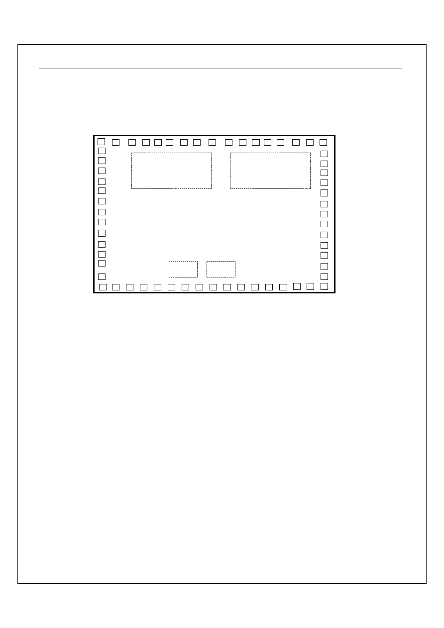
Chip size: 1890 x 1700 µm
* The chip substrate must be connected to GND (PAD 20)

ST2006
Ver 1.21
39/38
2003/
7/4
1
1
8
8
.
.
<Revisions>
Version 1.21 ≠ Page 2 modify block diagram
Page 34 modify values of standby current
Version 1.20 ≠ Page 33 modify Seg0-3 output current value.
≠ Page 36 Add 1/3 duty,1/2 bias application circuit.
Version 1.10 - Page 34 modify TABLE 15-32 R vs. OSC.
- Page 35 modify application 1 and application 2.
Version 0.91 - Page 35 increase bonding diagram.
- Page 33 Change DC supply voltage & temperature.
Version 0.9 - Page 2 modify Block Diagram.
- Change $3C(IREQ) power on default.
- Page 18 description of XSEL bit.
- Page 30 description of LCD frame clock.
Version 0.81 - Change $3A(LCTL) be write only register.