
ST
Sitronix
ST2016A
16K 8-bit Single Chip Microcontroller
Ver 1.4
1
/
53
11/11/03
1
1
.
.
F
F
E
E
A
A
T
T
U
U
R
R
E
E
S
S
8-bit static pipeline CPU
ROM: 16K x 8 bits
RAM: 192 x 8 bits
Operation voltage : 2.4V ~ 3.6V
24 CMOS Bi-directional bit programmable I/O pins
- Twenty (Port-A high nibble & Port-B/C) are shared with
LCD drives
6 Output pins (Four are shared with LCD common and
two are shared with PSG)
2 Input pins (code option: Shared with OSCX)
Hardware debounce option for input port
Bit programmable PULL-UP for input port
Timer/Counter
:
- One 8-bit timer / 16-bit event counter
- One 8-bit BASE timer
Five powerful interrupt sources :
- External interrupt (edge trigger)
- TIMER1 interrupt
- BASE timer interrupt
- PORTA[7~0] interrupt (transition trigger)
- DAC reload interrupt
32-level deep stack
Dual clock source :
- OSCX: Crystal oscillator: 32768Hz
- OSC: RC oscillator 500K ~ 4M Hz
Build-in oscillator with warm-up timer
LCD
controller
driver:
- 16 level contrast control
- 320 ( 8x40) dots ( 1/8 duty, 1/4 bias, programmable)
- 160 ( 4x40) dots ( 1/4 duty, 1/3 bias, programmable)
- Two clock source options: RC and resonator oscillator
- Keyboard scan function supported on 20 shared
segment drives
- Internal bias resistors(1/4 bias & 1/3 bias) with 32 level
driving strength control
Programmable Sound Generator (PSG) includes :
- Tone generator
- Sound effect generator
- 16 level volume control
- Digital DAC for speech / tone
Three power down modes :
- WAI0 mode
- WAI1 mode
- STP mode
2
2
.
.
G
G
E
E
N
N
E
E
R
R
A
A
L
L
D
D
E
E
S
S
C
C
R
R
I
I
P
P
T
T
I
I
O
O
N
N
ST2016A is a low-cost, high-performance, fully static, 8-bit
microcontroller designed with CMOS silicon gate
technology. It comes with 8-bit pipeline CPU core, SRAM,
timer, LCD driver, I/O port, PSG and mask program ROM. A
build-in dual oscillator is specially integrated to enhance
chip performance. For business equipment and consumer
applications. Such as watch, calculator, LCD game and IR
remote control, ST2016A is definitely a perfect solution for
implementation.

ST2016A
Ver 1.4
2/55
11/11/03
3
3
.
.
B
B
L
L
O
O
C
C
K
K
D
D
I
I
A
A
G
G
R
R
A
A
M
M
ST2016A
Ver 1.4
3/55
11/11/03
4
4
.
.
P
P
A
A
D
D
D
D
I
I
A
A
G
G
R
R
A
A
M
M
ST2016A
Ver 1.4
4/55
11/11/03
5
5
.
.
B
B
o
o
n
n
d
d
i
i
n
n
g
g
I
I
n
n
f
f
o
o
r
r
m
m
a
a
t
t
i
i
o
o
n
n
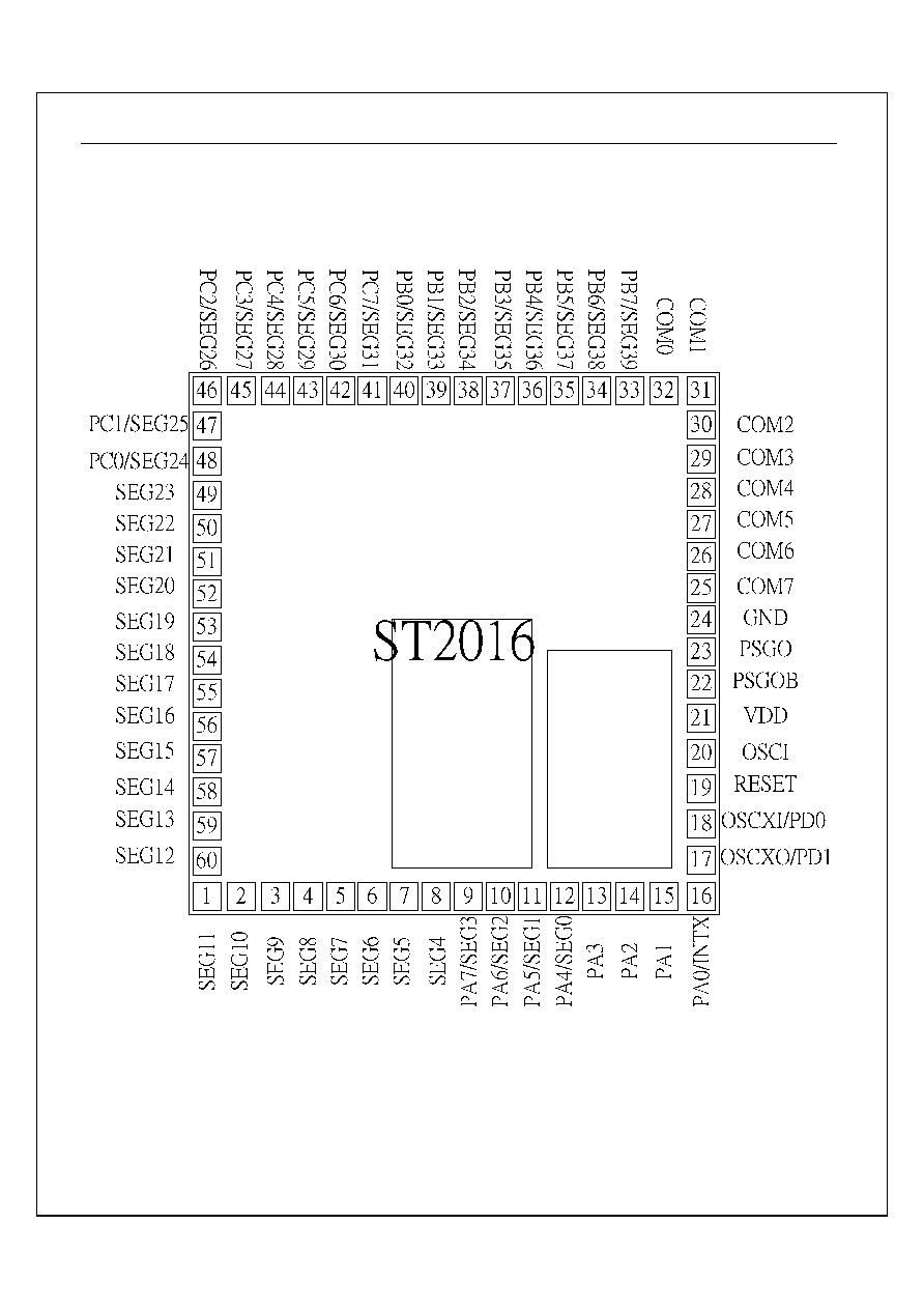
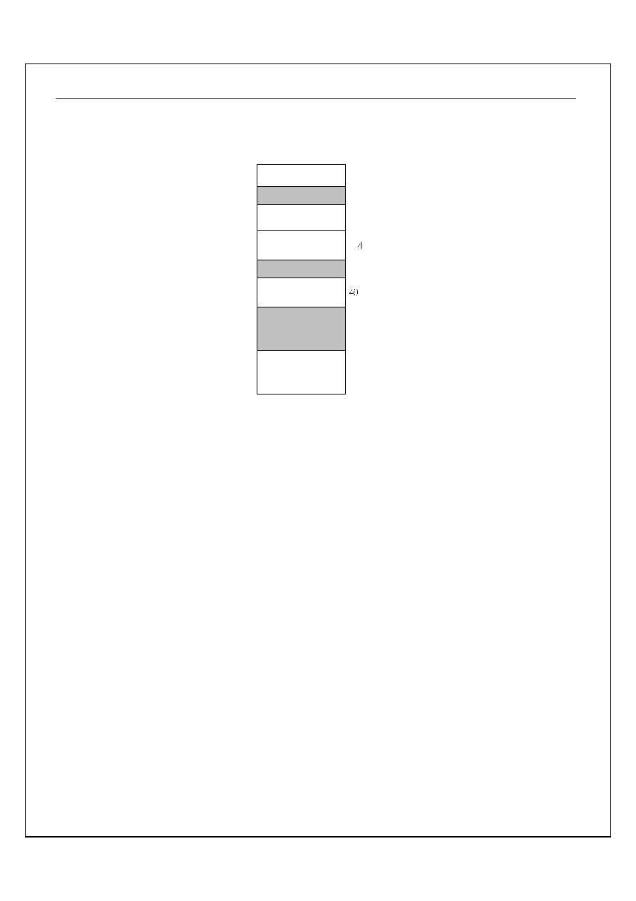
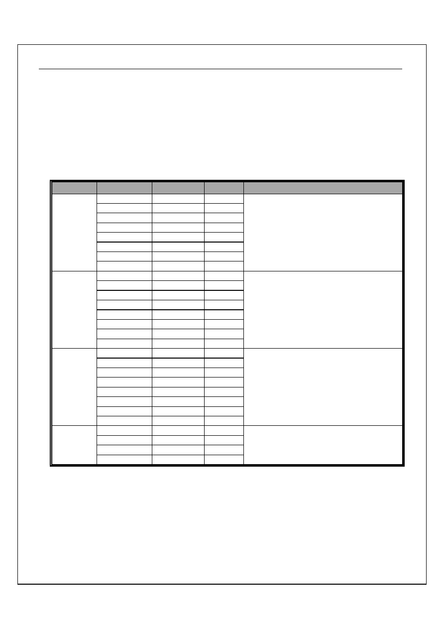
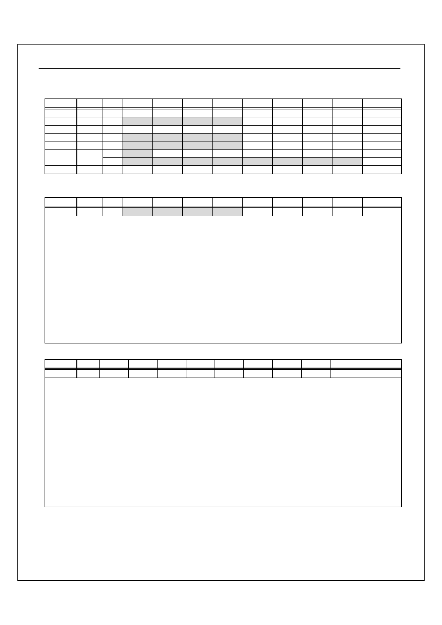
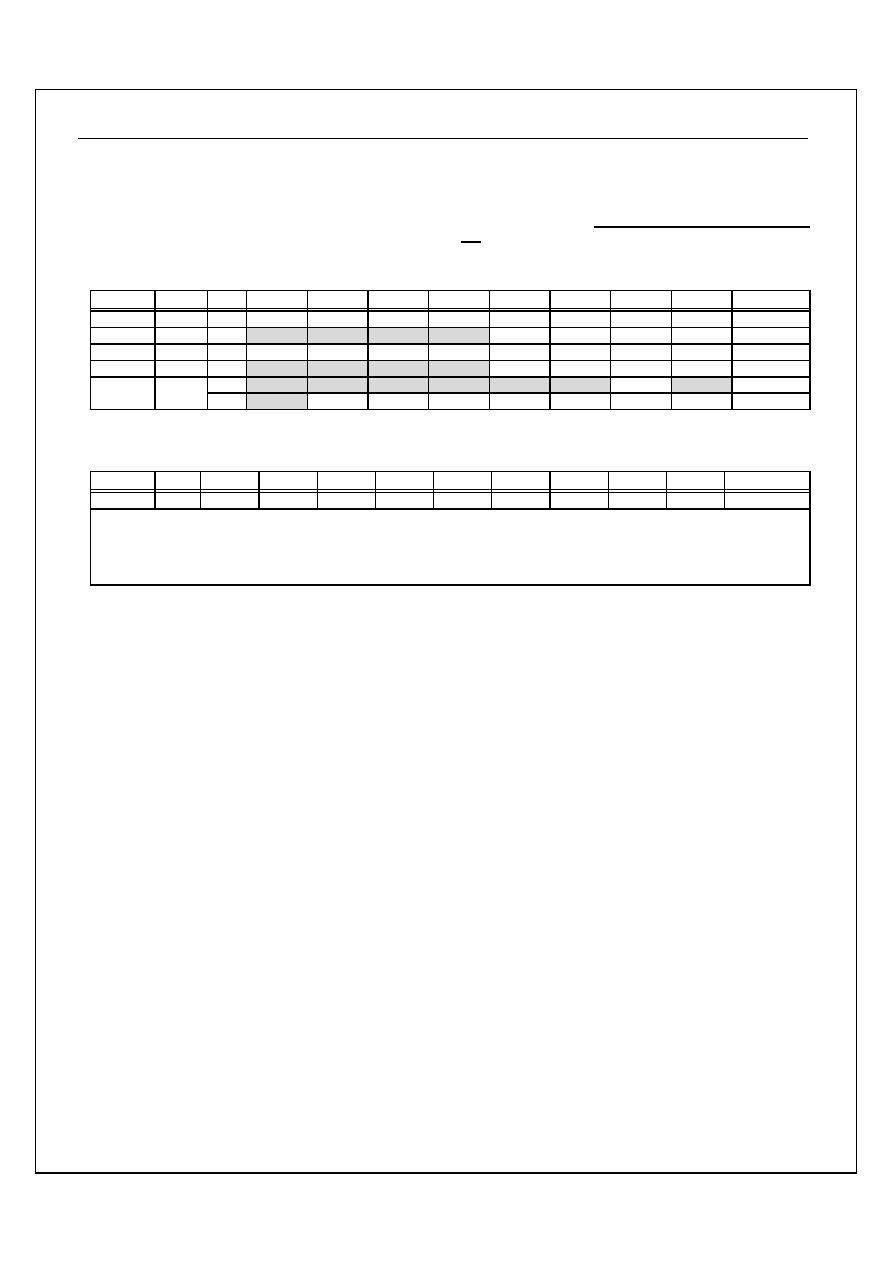
Chip Size: 1700 X 1740 �m
The chip substrate should be wired to GND pin.
Unit: �m
PAD CENTER
PAD CENTER
PAD #
NAME
X Y
PAD #
NAME
X Y
1 SEG11 57.5 57.5
31 COM1 1642.5 1682.5
2 SEG10 167.50 57.5 32 COM0 1522.50 1682.5
3 SEG9 277.50 57.5 33 PB7/SEG39 1412.50 1682.5
4 SEG8 382.50 57.5 34 PB6/SEG38 1307.50 1682.5
5 SEG7 486.25 57.5 35 PB5/SEG37 1203.75 1682.5
6 SEG6 588.75 57.5 36 PB4/SEG36 1101.25 1682.5
7 SEG5 691.25 57.5 37 PB3/SEG35 998.75 1682.5
8 SEG4 793.75 57.5 38 PB2/SEG34 896.25 1682.5
9 PA7/SEG3 896.25 57.5 39 PB1/SEG33 793.75 1682.5
10 PA6/SEG2 998.75 57.5 40 PB0/SEG32 691.25 1682.5
11 PA5/SEG1 1101.25 57.5 41 PC7/SEG31 588.75 1682.5
12 PA4/SEG0 1203.75 57.5 42 PC6/SEG30 486.25 1682.5
13 PA3 1307.5 57.5 43 PC5/SEG29 382.50 1682.5
14 PA2 1412.5 57.5 44 PC4/SEG28 277.50 1682.5
15 PA1 1522.5 57.5 45 PC3/SEG27 167.50 1682.5
16 PA0/INTX 1642.5 57.5 46 PC2/SEG26 57.5 1682.5
17 OSCXO/PD1 1642.5
175.35
47
PC1/SEG25 57.5
1568.70
18 OSCXI/PD0 1642.5
291.25
48
PC0/SEG24 57.5
1455.65
19 RESET 1642.5
405.25
49 SEG23
57.5
1347.35
20 OSCI 1642.5
518.25
50 SEG22
57.5
1240.30
21 VDD 1642.5
630.25
51 SEG21
57.5
1134.50
22 PSGOB 1642.5
741.25
52 SEG20
57.5
1028.70
23 PSGO 1642.5
843.75
53 SEG19
57.5
922.90
24 GND 1642.5
946.25
54 SEG18
57.5
817.10
25 COM7 1642.5
1048.75
55 SEG17
57.5
711.30
26 COM6 1642.5
1151.25
56 SEG16
57.5
605.50
27 COM5 1642.5
1253.75
57 SEG15
57.5
499.70
28 COM4 1642.5
1357.50
58 SEG14
57.5
392.65
29 COM3 1642.5
1462.50
59 SEG13
57.5
284.35
30 COM2 1642.5
1572.50
60 SEG12
57.5
171.30
ST2016A
Ver 1.4
5/55
11/11/03
6
6
.
.
P
P
A
A
D
D
D
D
E
E
S
S
C
C
R
R
I
I
P
P
T
T
I
I
O
O
N
N
Designation Pad
# Type
Description
SEG0/PA4 ~
SEG3/PA7
12 ~ 9
O
I/O
LCD Segment output
Port-A bit programmable I/O
SEG4 ~ SEG23
8 ~ 1
60 ~ 49
O
LCD Segment output
SEG24/PC0 ~
SEG31/PC7
48 ~ 41
O
I/O
LCD Segment output
Port-C bit programmable I/O
SEG32/PB0 ~
SEG39/PB7
40 ~ 33
O
I/O
LCD Segment output
Port-B bit programmable I/O
COM 0 � 3
32 ~ 29
O
LCD Common output
COM 4 - 7
28 ~ 25
O
O
LCD Common output
Output port
RESET
19
I
Pad reset input (HIGH Active)
GND
24
P
Ground Input and chip substrate
PA0/INTX 16
I/O
I
I
I
Port-A bit programmable I/O
Edge-trigger Interrupt.
Transition-trigger Interrupt
Programmable Timer1 clock source
PA 1-7
15 ~ 13
I/O
I
Port-A bit programmable I/O
Transition-trigger Interrupt
PSGO,PSGOB 23,22 O PSG/DAC
Output
V
DD
21 P
Power
supply
OSCXI/PD0 18
I
I
OSC input pin. For 32768Hz crystal
Port-D input
OSCXO/PD1 17
O
I
OSC output pin. For 32768Hz crystal
Port-D input
OSCI
20
I
OSC input pin. toward to external resistor
Legend: I = input, O = output, I/O = input/output, P = power.
ST2016A
Ver 1.4
6/55
11/11/03
7
7
.
.
C
C
P
P
U
U
7
0
A
7
0
Y
7
0
X
7
0
PCH PCL
8 7 6 5
0
1 0 0
S
Accumulator A
Index Register Y
Index Register X
Program Counter PC
Stack Pointer S
CPU REGISTER MODEL
7.1 Accumulator
(A)
The accumulator is a general purpose 8-bit register which
stores the results of most arithmetic and logic operations. In
addition, the accumulator usually contains one of the two
data words used in these operations.
7.2 Index Registers (X,Y)
There are two 8-bit Index Registers (X and Y) which may be
used to count program steps or to provide and index value to
be used in generating an effective address. When executing
an instruction which specifies indexed addressing, the CPU
fetches the OP code and the base address, and modifies the
address by adding the index register to it prior to performing
the desired operation. Pre or post-indexing of indirect
addresses is possible.
7.3 Stack Pointer (S)
The stack Pointer is an 8-bit register which is used to control
the addressing of the variable-length stack. It's range from
100H to 13FH total for 64 bytes (32-level deep). The stack
pointer is automatically incremented and decrement under
control of the microprocessor to perform stack
manipulations under direction of either the program or
interrupts (IRQ). The stack allows simple implementation of
nested subroutines and multiple level interrupts. The stack
pointer is initialized by the user's software.
7.4 Program Counter (PC)
The 16-bit Program Counter register provides the address
which step the microprocessor through sequential program
instructions. Each time the microprocessor fetches and
instruction from program memory, the lower byte of the
program counter (PCL) is placed on the low-order bits of the
address bus and the higher byte of the program counter
(PCH) is placed on the high-order 8 bits. The counter is
incremented each time an instruction or data is fetched from
program memory.
7.5 Status Register (P)
The 8-bit Processor Status Register contains seven status
flags. Some of the flags are controlled by the program,
others may be controlled both by the program and the CPU.
The instruction set contains a member of conditional branch
instructions which are designed to allow testing of these
flags.

ST2016A
Ver 1.4
7/55
11/11/03
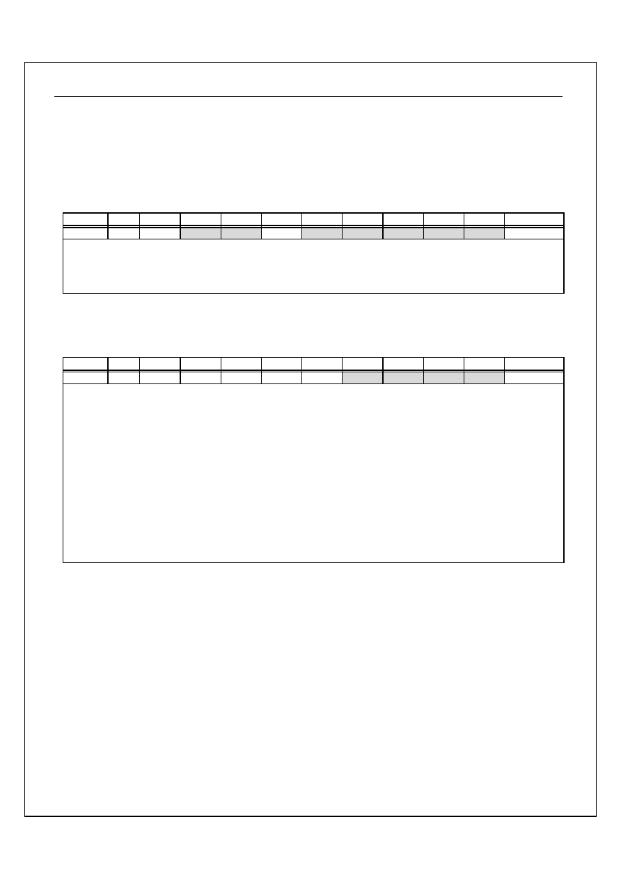
TABLE 7-1: STATUS REGISTER (P)
Bit 7
Bit 6
Bit 5
Bit 4
Bit 3
Bit 2
Bit 1
Bit 0
N V 1 B D I Z C
Bit 7: N : Signed flag by arithmetic
1 = Negative
0 = Positive
Bit 6: V : Overflow of signed Arithmetic flag
1 = Negative
0 = Positive
Bit 4: B : BRK interrupt flag *
1 = BRK interrupt occur
0 = Non BRK interrupt occur
Bit 3: D : Decimal mode flag
1 = Decimal mode
0 = Binary mode
Bit 2: I : Interrupt disable flag
1 = Interrupt disable
0 = Interrupt enable
Bit 1: Z : Zero flag
1 = Zero
0 = Non zero
Bit 0: C : Carry flag
1 = Carry
0 = Non carry
ST2016A
Ver 1.4
8/55
11/11/03
8
8
.
.
M
M
E
E
M
M
O
O
R
R
Y
Y
C
C
O
O
N
N
F
F
I
I
G
G
U
U
R
R
A
A
T
T
I
I
O
O
N
N
User RAM
0080H
00FFH
128 BYTE
No Use
0040H
007FH
I/
0000H
003FH
64 BYTES
No Use
0228H
BFFFH
RO
C000H
FFFFH
16K BYTE
STACK RAM&
User RAM
0100H
013FH
64 BYT
LCD RA
0200H
0227H
0 BYTE
No Use
0140H
01FFH
8.1 ROM
($C000~$FFFF)
The ST2016A has 16K bytes ROM used for program, data and vector address.
Vector address mapping :
$FFFE
Software BRK operation vector..
$FFFC RESET
vector.
$FFFA Reserved.
$FFF8
INTX (PA0) edge interrupter.
$FFF6
Reload DAC data interrupter.
$FFF4 Reserved.
$FFF2 Timer1
interrupter.
$FFF0 PORTA
transition
interrupter.
$FFEE Base
Timer
interrupter.
ST2016A
Ver 1.4
9/55
11/11/03
8.2 RAM
The RAM mapping includes Control Registers, Data RAM, Stack RAM and LCD RAM.
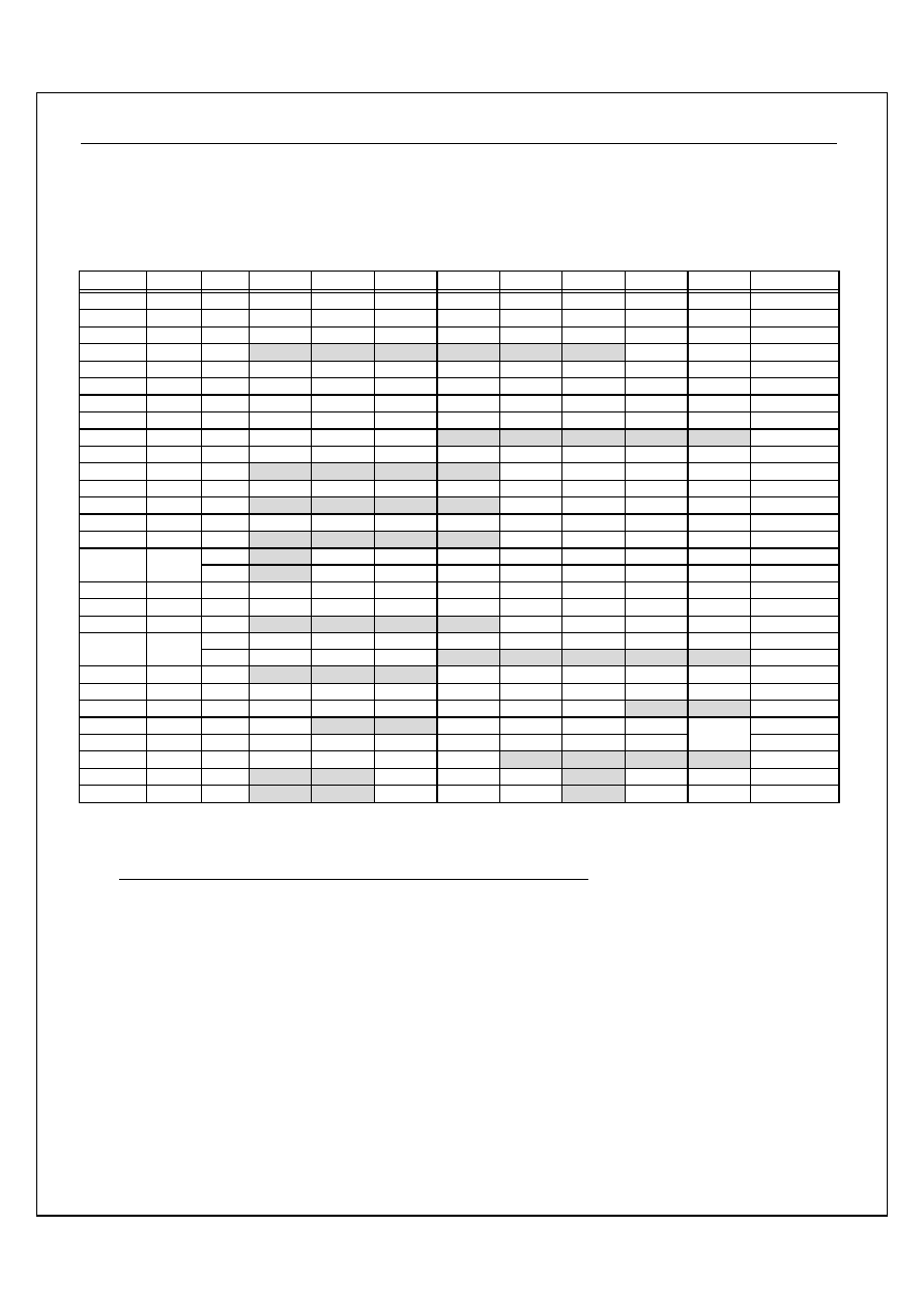
TABLE 8-2: CONTROL REGISTERS ($0000~$003E)
Address Name R/W
Bit 7
Bit 6
Bit 5
Bit 4
Bit 3
Bit 2
Bit 1
Bit 0
Default
$000 PA
R/W PA[7] PA[6] PA[5] PA[4] PA[3] PA[2] PA[1] PA[0] 1111
1111
$001 PB
R/W PB[7] PB[6] PB[5] PB[4] PB[3] PB[2] PB[1] PB[0] 1111
1111
$002 PC
R/W PC[7] PC[6] PC[5] PC[4] PC[3] PC[2] PC[1] PC[0] 1111
1111
$003 PD
R/W
-
-
-
-
-
-
PD[1]
PD[0]
- - - - - - 11
$008 PCA R/W PCA[7] PCA[6] PCA[5] PCA[4] PCA[3] PCA[2] PCA[1] PCA[0] 0000
0000
$009 PCB R/W PCB[7] PCB[6] PCB[5] PCB[4] PCB[3] PCB[2] PCB[1] PCB[0] 0000
0000
$00A PCC R/W PCC[7] PCC[6] PCC[5] PCC[4] PCC[3] PCC[2] PCC[1] PCC[0] 0000
0000
$00E PAK R/W PAK[7] PAK[6] PAK[5] PAK[4] PAK[3] PAK[2] PAK[1] PAK[0] 0000
0000
$00F PMCR R/W PULL PDBN INTEG
-
-
-
-
-
100 - - - - -
$010 PSG0L R/W PSG0[7] PSG0[6] PSG0[5] PSG0[4] PSG0[3] PSG0[2] PSG0[1] PSG0[0] 0000 0000
$011 PSG0H R/W
-
-
-
-
PSG0[11] PSG0[10]
PSG0[9] PSG0[8] - - - - 0000
$012 PSG1L R/W PSG1[7] PSG1[6] PSG1[5] PSG1[4] PSG1[3] PSG1[2] PSG1[1] PSG1[0] 0000 0000
$013 PSG1H R/W
-
-
-
-
PSG1[11] PSG1[10]
PSG1[9] PSG1[8] - - - - 0000
$014 DAC R/W DAC[7] DAC[6] DAC[5] DAC[4] DAC[3] DAC[2] DAC[1] DAC[0] 0000
0000
$015 PSGC2 R/W
-
-
-
-
PSGOD PSGOBD PSGOE PSGOBE - - - - 1111
R/W
-
PCK[2] PCK[1] PCK[0] PRBS C1EN C0EN DACE=0
-000
0000
$016 PSGC
R/W
-
PCK[2] PCK[1] PCK[0] DMD[1] DMD[0] INH DACE=1
-000
0000
$017 VOL R/W VOL1[3] VOL1[2] VOL1[1] VOL1[0] VOL0[3] VOL0[2] VOL0[1] VOL0[0]
0000
0000
$020 LCK R/W
DRV[4] DRV[3] DRV[2] DRV[1] DRV[0] LCK[2] LCK[1] LCK[0]
0000
0100
$021 BTM R/W
-
-
-
- BTM[3]
BTM[2]
BTM[1]
BTM[0]
- - - - 0000
R PRS[7] PRS[6] PRS[5] PRS[4] PRS[3] PRS[2] PRS[1] PRS[0] 0000
0000
$023 PRS
W SRES SENA SENT -
-
-
-
-
000 - - - - -
$026 T1M R/W
-
-
- T1M[4]
T1M[3]
T1M[2]
T1M[1]
T1M[0]
- - -0 0000
$027 T1C
R/W T1C[7] T1C[6] T1C[5] T1C[4] T1C[3] T1C[2] T1C[1] T1C[0] 0000
0000
$030 SYS R/W XSEL OSTP XSTP XBAK WSKP WAIT
-
-
0000 00- -
$039 LSEL R/W LSEL[7]
-
-
LSEL[4] LSEL[3] LSEL[2] LSEL[1] LSEL[0] 1 - -1 1111
$03A LCTL W LPWR BLANK DUTY SCAN CTR[3] CTR[2] CTR[1] CTR[0] 1000
0000
$03B COM R/W COM[7] COM[6] COM[5] COM[4]
-
-
-
-
0000 - - - -
$03C IREQ R/W
-
- IRBT
IRPT
IRT1 -
IRDAC
IRX
- - 11 1-11
$03E IENA R/W
-
- IEBT
IEPT
IET1 -
IEDAC
IEX
- - 00 0-00
Note: 1. Some addresses of I/O area, $3~$7, $B~$E, $15, $18~$1F, $22, $24~$25, $28~$2F, $31~ $39,
$3D,$3F, are no used.
2. User should never use undefined addresses and bits.
3. Do not use Bit instructions for write-only registers, such as RMBx, SMBx....
4. E.V.B `s RAM Power On Initial Value are Same as Real Chip.
8.2.2
DATA RAM ($0080~$00FF)
DATA RAM are organized in 128 bytes.
8.2.3
STACK RAM ($0100~$013F)
STACK RAM are organized in 64 bytes. It provides for a
maximum of 32-level subroutine stacks And can be used as
data memory.
8.2.4 LCD RAM ($0200~$0227)
Resident LCD-RAM, accessible through write and read
instructions, are organized in 40 bytes for 40x8 LCD display.
Note that this area can also be used as data memory.
ST2016A
Ver 1.4
10/55
11/11/03
9
9
.
.
I
I
N
N
T
T
E
E
R
R
R
R
U
U
P
P
T
T
S
S
TABLE 9-3: PREDEFINED VECTORS FOR INTERRUPT
Name
Name
Name
Name
Signal
Signal
Signal
Signal
Vector address
Vector address
Vector address
Vector address
Priority
Comment
Comment
Comment
Comment
BRK
Internal
$FFFF,$FFFE
8
Software BRK operation vector
RESET External
$FFFD,$FFFC
1
RESET vector
-
-
$FFFB,$FFFA
-
Reserved
INTX External $FFF9,$FFF8 2
PA0 edge interrupt
DAC Internal $FFF7,$FFF6 3
Reload DAC data interrupt
-
-
$FFF5,$FFF4
-
Reserved
T1 INT/EXT $FFF3,$FFF2 4
Timer1 interrupt
PT External $FFF1,$FFF0 5
Port-A transition interrupt
BT Internal $FFEF,$FFEE 6
Base Timer interrupt
9.2 Interrupt
description
Brk
Instruction `BRK' will cause software interrupt when interrupt
disable flag (I) is cleared. Hardware will push `PC', `P '
Register to stack and set interrupt disable flag (I). Program
counter then will be loaded with the BRK vector from
locations $7FFE and $7FFF.
RESET
A positive transition of RESET pin will then cause an
initialization sequence to begin. After the system has been
operating, a high on this line of a least two clock cycles will
cease ST2016AST2016A activity. When a positive edge is
detected, there is an initialization sequence lasting six clock
cycles. Then the interrupt mask flag is set, the decimal mode
is cleared and the program counter will loaded with the
restart vector from locations $FFFC (low byte) and $FFFD
(high byte). This is the start location for program control.
This input should be low in normal operation.
INTX interrupt
The IRX (INTX interrupt request) flag will be set while INTX
edge signal occurs. The INTX interrupt will be active once
IEX (INTX interrupt enable) is set, and interrupt mask flag is
cleared. Hardware will push `PC', `P' Register to stack and
set interrupt mask flag (I). Program counter will be loaded
with the INTX vector from locations $FFF8 and $FFF9.
DAC interrupt
The IRDAC (DAC interrupt request) flag will be set while
reload signal of DAC occurs. Then the DAC interrupt will be
executed when IEDAC (DAC interrupt enable) is set, and
interrupt mask flag is cleared. Hardware will push `PC', `P'
Register to stack and set interrupt mask flag (I). Program
counter will be loaded with the DAC vector from locations
$FFF6 and $FFF7.
T1 interrupt
The IRT1 (TIMER1 interrupt request) flag will be set while T1
overflows. With IET1 (TIMER1 interrupt enable) being set,
the T1 interrupt will executed, and interrupt mask flag will be
cleared. Hardware will push `PC', `P' Register to stack and
set interrupt mask flag (I). Program counter will be loaded
with the T1 vector from locations $FFF2 and $FFF3.
PT interrupt
The IRPT (Port-A interrupt request) flag will be set while
Port-A transition signal occurs. With IEPT (PT interrupt
enable)being set, the PT interrupt will be execute, and
interrupt mask flag will be cleared. Hardware will push `PC',
`P' Register to stack and set interrupt mask flag (I). program
counter will be loaded with the PT vector from locations
$FFF0 and $FFF1.
BT interrupt
The IRBT (Base timer interrupt request) flag will be set when
Base Timer overflows. The BT interrupt will be executed
once the IEBT (BT interrupt enable) is set and the interrupt
mask flag is cleared. Hardware will push `PC', `P' Register
to stack and set interrupt mask flag (I). Program counter will
be loaded with the BT vector from locations $FFEE and
$FFEF.
ST2016A
Ver 1.4
11/55
11/11/03
9.3 Interrupt
request
clear
Interrupt request flag can be cleared by two methods. One is
to write "0" to IENA, the other is to initiate the interrupt
service routine when interrupt occurs. Hardware will
automatically clear the Interrupt flag.
TABLE 9-4: INTERRUPT REQUEST REGISTER (IREQ)
Address Name R/W
Bit 7
Bit 6
Bit 5
Bit 4
Bit 3
Bit 2
Bit 1
Bit 0
Default
$03C IREQ R/W
-
- IRBT
IRPT
IRT1 -
IRDAC
IRX
- - 11 1-11
Bit 5: IRBT: Base Timer Interrupt Request bit
1 = Time base interrupt occurs
0 = Time base interrupt doesn't occur
Bit 4: IRPT: Port-A Interrupt Request bit
1 = Port-A transition interrupt occurs
0 = Port-A transition interrupt doesn't occur
Bit 3: IRT1: Timer1 Interrupt Request bit
1 = Timer1 overflow interrupt occurs
0 = Timer1 overflow interrupt doesn't occur
Bit 1: IRDAC: DAC reload Interrupt Request bit
1 = DAC time out interrupt occurs
0 = DAC time out interrupt doesn't occur
Bit 0: IRX: INTX Interrupt Request bit
1 = INTX edge interrupt occurs
0 = INTX edge interrupt doesn't occur
TABLE 9-5: INTERRUPT ENABLE REGISTER (IENA)
Address Name R/W
Bit 7
Bit 6
Bit 5
Bit 4
Bit 3
Bit 2
Bit 1
Bit 0
Default
$03E IENA R/W
-
- IEBT
IEPT
IET1 -
IEDAC
IEX
- - 00 0-00
Bit 5: IEBT: Base Timer Interrupt Enable bit
1 = Time base interrupt enable
0 = Time base interrupt disable
Bit 4: IEPT: Port-A Interrupt Enable bit
1 = Port-A transition interrupt enable
0 = Port-A transition interrupt disable
Bit 3: IET1: Timer1 Interrupt Enable bit
1 = Timer1 overflow interrupt enable
0 = Timer1 overflow interrupt disable
Bit 1: IEDAC: DAC reload Interrupt Enable bit
1 = DAC time out interrupt enable
0 = DAC time out interrupt disable
Bit 0: IEX: INTX Interrupt Enable bit
1 = INTX edge interrupt enable
0 = INTX edge interrupt disable
ST2016A
Ver 1.4
12/55
11/11/03
1
1
0
0
.
.
I
I
/
/
O
O
P
P
O
O
R
R
T
T
S
S
ST2016A can supply total 24 GPIOs divided into three I/O
ports, Port-A, Port-B, and Port-C. Besides I/O function,
Port-B/C & Port-A's high nibble can also be used as LCD
segment drives. For detail pin assignment, please refer to
TABLE 10-6:
TABLE 10-6: I/O DESCRIPTION
PORT NAME
PAD NAME
PAD NUMBER PIN TYPE
FEATURE
PA0/INTX 16 I/O
PA1 15
I/O
PA2 14
I/O
PA3 13
I/O
PA4/SEG0 12 I/O
PA5/SEG1 11 I/O
PA6/SEG2 10 I/O
Port-A
PA7/SEG3 9 I/O
Programmable input/output pin
SEG32/PB0 40 I/O
SEG33/PB1 39 I/O
SEG34/PB2 38 I/O
SEG35/PB3 37 I/O
SEG36/PB4 36 I/O
SEG37/PB5 35 I/O
SEG38/PB6 34 I/O
Port-B
SEG39/PB7 33 I/O
Programmable input/output pin
SEG24/PC0 48 I/O
SEG25/PC1 47 I/O
SEG26/PC2 46 I/O
SEG27/PC3 45 I/O
SEG28/PC4 44 I/O
SEG29/PC5 43 I/O
SEG30/PC6 42 I/O
Port-C
SEG31/PC7 41 I/O
Programmable input/output pin
COM4 28 O
COM5 27 O
COM6 26 O
COM[4~7]
COM7 25 O
Programmable output pin
ST2016A
Ver 1.4
13/55
11/11/03
10.2 PORT-A
Port-A is a bit-programmable bi-direction I/O port, which is
controlled by PCA register. It also provides bit programmable
pull-up resistor for each input pin. Two interrupts can be
triggered by Port-A, de-bounced interrupt for keyboard scan and
edge sensitive interrupt (PA0 only) for external event. Four of
these I/Os can change into LCD segment drives. LSEL[7] of
control register LSEL specifies which of these I/Os are LCD
drives(Please refer to 15.4.1.1 LCD Segment Number Selection
Register (LSEL)).
TABLE 10-7: SUMMARY FOR PORT-A REGISTERS
Address Name R/W
Bit 7
Bit 6
Bit 5
Bit 4
Bit 3
Bit 2
Bit 1
Bit 0
Default
$000 PA
R/W PA[7] PA[6] PA[5] PA[4] PA[3] PA[2] PA[1] PA[0] 1111
1111
$008 PCA R/W PCA[7] PCA[6] PCA[5] PCA[4] PCA[3] PCA[2] PCA[1] PCA[0] 0000
0000
$00E PAK R/W PAK[7] PAK[6] PAK[5] PAK[4] PAK[3] PAK[2] PAK[1] PAK[0] 0000
0000
$00F PMCR R/W PULL PDBN
INTEG -
-
-
-
-
100 - - - - -
$03C IREQ R/W
-
-
IRBT IRPT IRT1
-
IRDAC
IRX
- - 11 1-11
$03E IENA R/W
-
-
IEBT IEPT IET1
-
IEDAC
IEX
- - 00 0-00
$039 LSEL R/W
LSEL[7]
-
-
LSEL[4] LSEL[3] LSEL[2] LSEL[1] LSEL[0] 1 - -1 1111
10.2.2 PORT-A
I/O
control
Direction of Port-A is controlled by PCA. Every bit of
PCA[7~0] is mapped to the I/O direction of PA[7~0]
correspondingly, with "1" for output mode, and "0" for input
mode.
TABLE 10-8: PORT-A CONTROL REGISTER (PCA)
Address Name R/W
Bit 7
Bit 6
Bit 5
Bit 4
Bit 3
Bit 2
Bit 1
Bit 0
Default
$008 PCA R/W PCA[7] PCA[6] PCA[5] PCA[4] PCA[3] PCA[2] PCA[1] PCA[0] 0000
0000
Bit 7~0: PCA[7~0] : Port-A directional bits
1 = Output mode
0 = Input mode
10.2.3 Port-A used as keyboard return line
When LCD Keyboard Awaking Pulses function is enabled
(Please refer to 15.6 Keyboard-scan Function on LCD drives),
the LCD waveform is always affected by Port-A signal if
Port-A was used as keyboard return line and any key was
being pressed. In order to reduce the effect from port-A, PAK
register must be set. The function will active when LCD on ,
LCD keyboard awaking pulses enable and PAK[7~0] is set to
"1".
TABLE 10-9: Port-A used as keyboard return line selection
Address Name
R/W
Bit 7
Bit 6
Bit 5
Bit 4
Bit 3
Bit 2
Bit 1
Bit 0
Default
$00E PAK R/W
PAK[7] PAK[6] PAK[5] PAK[4] PAK[3] PAK[2] PAK[1] PAK[0] 0000
0000
Bit 7~0: PAK[7~0] :
1 = Port-A used as keyboard return line.
0 = Port-A used as keyboard normal I/O.
ST2016A
Ver 1.4
14/55
11/11/03
10.2.4 PORT-A PULL-UP
OPTION
PORT-A contains pull-up MOS transistors controlled by
software. When an I/O is used as an input. The ON/OFF of
the pull-up MOS transistor will be controlled by port data
register (PA) and the pull-up MOS will be enabled with "1"
for data bit and disable with "0" for data bit. The PULL
control bit of PMCR controls the ON/OFF of all the pull-up
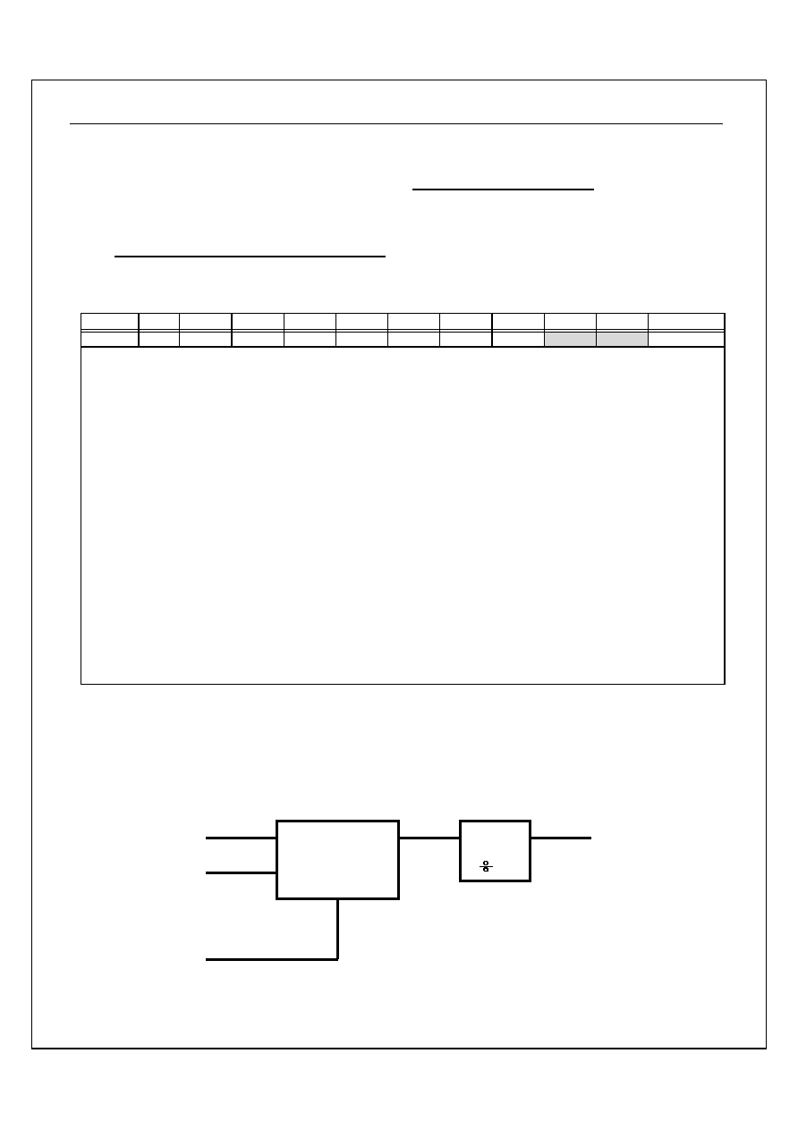
MOS simultaneously. Please refer to the Figure 9-1.
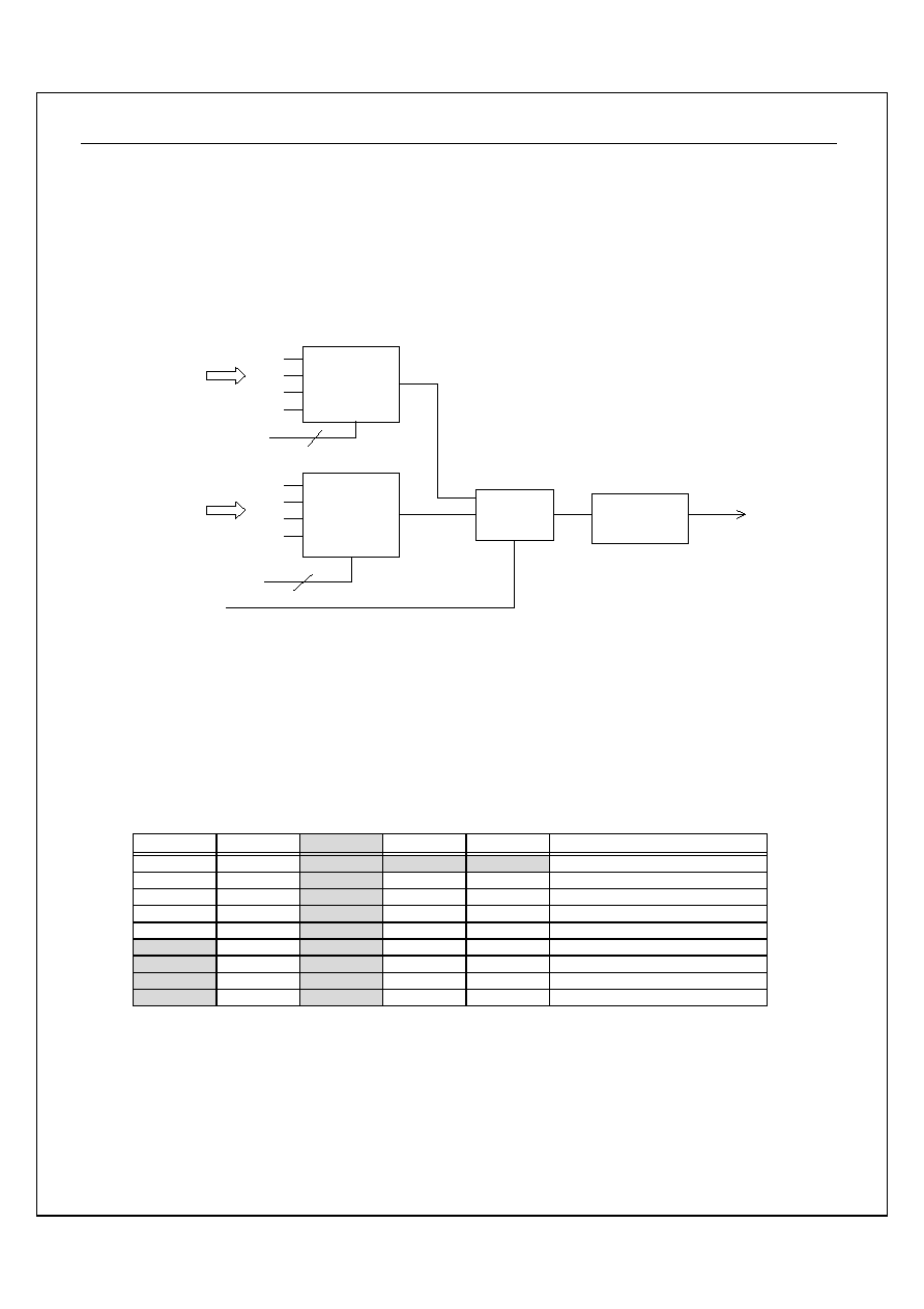
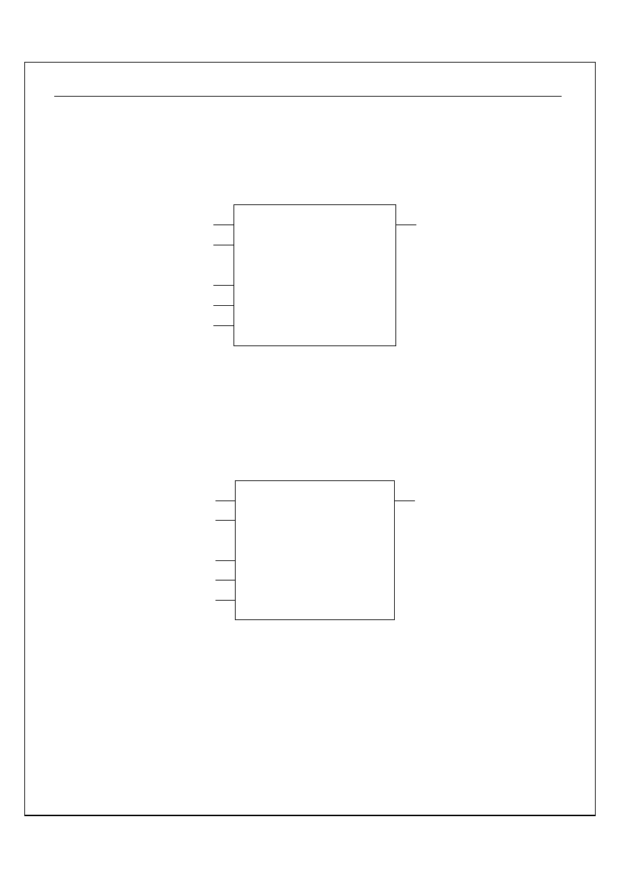
FIGURE 10-1: Port-A Configuration Function Block Diagram
VCC
PORT
DATA
REGISTER
( PDR )
PULL-UP
PMOS
PULL-UP
RD_INPUT
DATA INPUT
PORT
CONTROL
REGISTER
( PCR )
TABLE 10-10: PORT CONDITION CONTROL REGISTER (PMCR)
Address Name R/W
Bit 7
Bit 6
Bit 5
Bit 4
Bit 3
Bit 2
Bit 1
Bit 0
Default
$00F PMCR R/W PULL PDBN
INTEG -
-
-
-
-
100 - - - - -
Bit 7: PULL : Enable all pull-up function bit
1 = Enable pull-up function
0 = Disable pull-up function
Bit 6: PDBN : Enable Port-A interrupt debounce bit
1 = Debounce for Port-A interrupt
0 = No debounce for Port-A interrupt
Bit 5: INTEG : INTX interrupt edge select bit
1 = Rising edge
0 = Falling edge
ST2016A
Ver 1.4
15/55
11/11/03
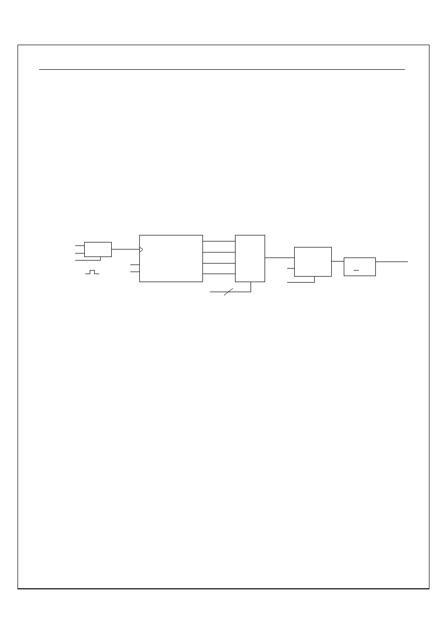
10.2.5 Port-A interrupt
Port-A, a programmable I/O, can be used as a port interrupt
when it is in the input mode. Any edge transition of the
Port-A input pin will generate an interrupt request. The last
state of Port-A must be kept before I/O transition and this
can be accomplished by reading Port-A.
When programmer enables INTX and PT interrupts, PA0
trigger occur. INTX and PT interrupts will therefore happen
sequentially. Please refer to the Figure 9-2.
Operating Port-A interrupt step by step :
1. Set input mode.
2. Read Port-A.
3. Clear interrupt request flag (IRPT).
4. Set interrupt enable flag (IEPT).
5. Clear CPU interrupt disable flag (I).
6. Read Port-A before `RTI' instruction in
INT-Subroutine.
Example :
.
.
.
STZ
PCA
;Set input mode.
LDA #$FF
STA
PA
;PA be PULL-UP.
LDA
PA
;Keep last state.
RMB4 <IREQ
;Clear
IRQ
flag.
SMB4 <IENA
;Enable
INT.
CLI
.
.
INT-SUBROUTINE
.
.
LDA
PA
;Keep last state.
RTI
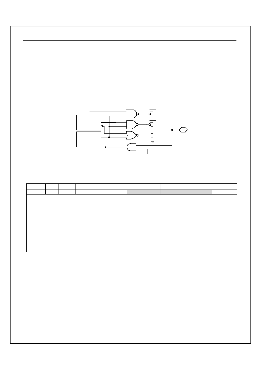
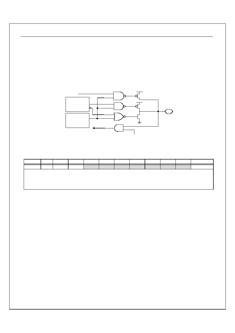
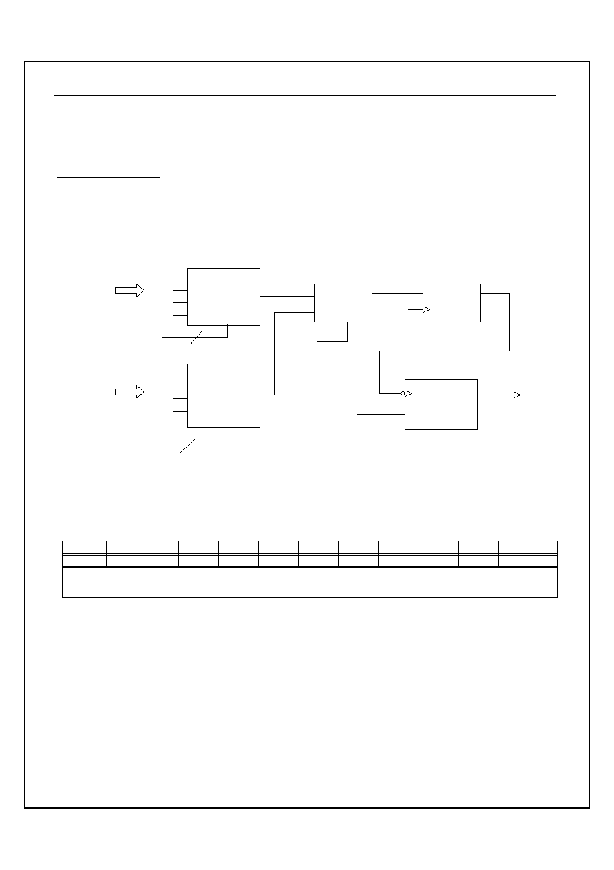
FIGURE 10-2: Port Interrupt Logic Diagram
NAND8
OR2
OR2
OR2
OR2
OR2
OR2
OR2
OR2
DFF
CK
D
Q
DFF
CK
D
Q
DFF
CK
D
Q
DFF
CK
D
Q
DFF
CK
D
Q
DFF
CK
D
Q
DFF
CK
D
Q
DFF
CK
D
Q
XNOR2
XNOR2
XNOR2
XNOR2
XNOR2
XNOR2
XNOR2
XNOR2
RDPA
PA[0]
PA[4]
PCA[0]
PCA[4]
PA[1]
PA[5]
PCA[1]
PCA[5]
PA[2]
PA[6]
PCA[2]
PCA[6]
PA[3]
PA[7]
PCA[3]
PCA[7]
PTIR
High Level Interrupt
ST2016A
Ver 1.4
16/55
11/11/03
10.2.5.2
Port-A interrupt debounce
ST2016A has hardware debounce option for Port-A
interrupt. The debounce will be enabled with "1" and disable
with "0" for PDBN. The debounce will active when Port-A
transition occurs, PDBN enable and OSCX enable.
The debounce time is OSCX x 512 cycles(about 16 ms).
Refer to the TABLE 9-10.
TABLE 10-11: PORT CONDITION CONTROL REGISTER (PMCR)
Address Name R/W
Bit 7
Bit 6
Bit 5
Bit 4
Bit 3
Bit 2
Bit 1
Bit 0
Default
$00F PMCR R/W
PULL PDBN INTEG
-
-
-
-
-
100 - - - - -
Bit 6: PDBN : Enable Port-A interrupt debounce bit
1 = Debounce for Port-A interrupt
0 = No debounce for Port-A interrupt
10.2.6 PA0/INTX
PA0 can be used as an external interrupt input(INTX).
Falling or Rising edge is controlled by INTEG(PMCR[5]) and
the external interrupt is set up with "0" for falling edge and "1"
for rising edge. Please refer to the Figure 9-3.
When programmer enables INTX and PT interrupts, PA0
trigger will occur. Both INTX and PT interrupts will happen
sequentially. Pelase refer to the operating steps.
Operating INTX interrupt step by step :
1.
Set PA0 pin into input mode. (PCA[0])
2.
Select edge level. (INTEG)
3.
Clear INTX interrupt request flag. (IRX)
4.
Set INTX interrupt enable bits. (IEX)
5.
Clear CPU interrupt mask flag (I).
Example :
.
.
.
RMB0 <PCA
;Set
input
mode.
SMB5 <PMCR
;Rising
edge.
RMB0 <IREQ
;Clear
IRQ
flag.
SMB0 <IENA
;Enable
INTX
interrupt.
CLI
.
.
.
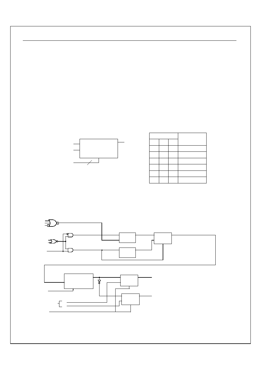
FIGURE 10-3: INTX Logic Diagram
PMCR[5]
PA 0/INTX
Falling Edge Interrupt
ST2016A
Ver 1.4
17/55
11/11/03
10.3 Port-B and Port-C
10.3.1 General Description
Port-B and Port-C are bit-programmable bi-direction I/O
ports, controlled by PCB and PCC registers. There is also bit
programmable pull-up resistor for each input pin. All of the 16
I/Os can change into LCD segment drives. Control register
LSEL specifies which of these I/Os are LCD drives(Please
refer to 15.4.1.1 LCD Segment Number Selection Register
(LSEL)).
TABLE 10-12: Summary of Port-B AND Port-C Registers
Address Name
R/W
Bit 7
Bit 6
Bit 5
Bit 4
Bit 3
Bit 2
Bit 1
Bit 0
Default
$001 PB
R/W PB[7] PB[6] PB[5] PB[4] PB[3] PB[2] PB[1] PB[0]
1111
1111
$002 PC
R/W PC[7] PC[6] PC[5] PC[4] PC[3] PC[2] PC[1] PC[0]
1111
1111
$009 PCB R/W PCB[7] PCB[6] PCB[5] PCB[4] PCB[3] PCB[2] PCB[1] PCB[0]
0000
0000
$00A PCC R/W PCC[7] PCC[6] PCC[5] PCC[4] PCC[3] PCC[2] PCC[1] PCC[0]
0000
0000
$00F PMCR R/W PULL PDBN
INTEG
-
-
-
-
-
100 - - - - -
$039 LSEL R/W
LSEL[7]
-
-
LSEL[4] LSEL[3] LSEL[2] LSEL[1] LSEL[0] 1 - - 1 1111
10.3.2 Input/Output
Control
PCB/PCC controls the I/O direction of Port-B/C. Each bit of
PCB[7~0]/PCC[7~0] controls the direction of one single bit of
Port-B/C respectively, with "1" for output mode, and "0" for
input mode.
TABLE 10-13: PORT-B Control Register (PCB)
Address Name
R/W
Bit 7
Bit 6
Bit 5
Bit 4
Bit 3
Bit 2
Bit 1
Bit 0
Default
$009 PCB R/W PCB[7] PCB[6] PCB[5] PCB[4] PCB[3] PCB[2] PCB[1] PCB[0]
0000
0000
Bit 7~0: PCB[7~0] : Port-B directional bits
1 = Output mode
0 = Input mode
TABLE 10-14: PORT-C Control Register (PCC)
Address Name
R/W
Bit 7
Bit 6
Bit 5
Bit 4
Bit 3
Bit 2
Bit 1
Bit 0
Default
$00A PCC R/W PCC[7] PCC[6] PCC[5] PCC[4] PCC[3] PCC[2] PCC[1] PCC[0]
0000
0000
Bit 7~0: PCC[7~0] : Port-C directional bits
1 = Output mode
0 = Input mode
ST2016A
Ver 1.4
18/55
11/11/03
10.3.3 Port-B and Port-C PULL-UP option
Port-B/C contains PMOS transistors of pull-up resistor
controlled by software in bit-manner. In case of input
direction, on/off of the pull-up PMOS transistor is controlled
by the data wrote to data register, PB/PC. "1" is for enable
and "0" is for disable. Above all, whole pull-up control is by
PULL bit of PMCR. Refer to FIGURE 10-4: for the block
description.
FIGURE 10-4: Port-B and Port-C Block Diagram
VCC
PORT
DATA
REGISTER
( PDR )
PULL-UP
PMOS
PULL-UP
RD_INPUT
DATA INPUT
PORT
CONTROL
REGISTER
( PCR )
TABLE 10-15: Port Control Register (PMCR)
Address Name R/W
Bit 7
Bit 6
Bit 5
Bit 4
Bit 3
Bit 2
Bit 1
Bit 0
Default
$00F PMCR R/W PULL PDBN
INTEG
-
-
-
-
-
100 - - - - -
Bit 7: PULL : Enable all pull-up functions bit
1 = Enable pull-up function
0 = Disable pull-up function
ST2016A
Ver 1.4
19/55
11/11/03
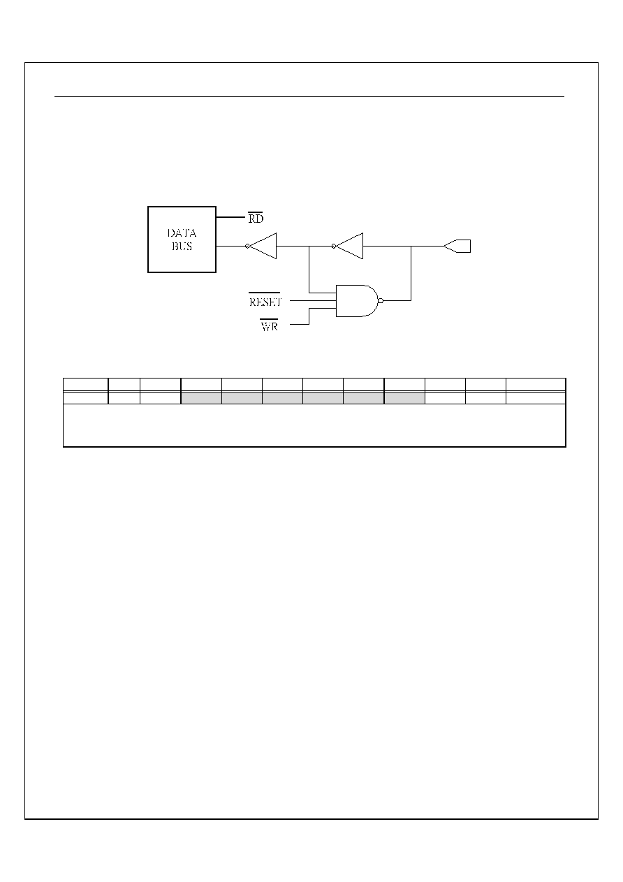
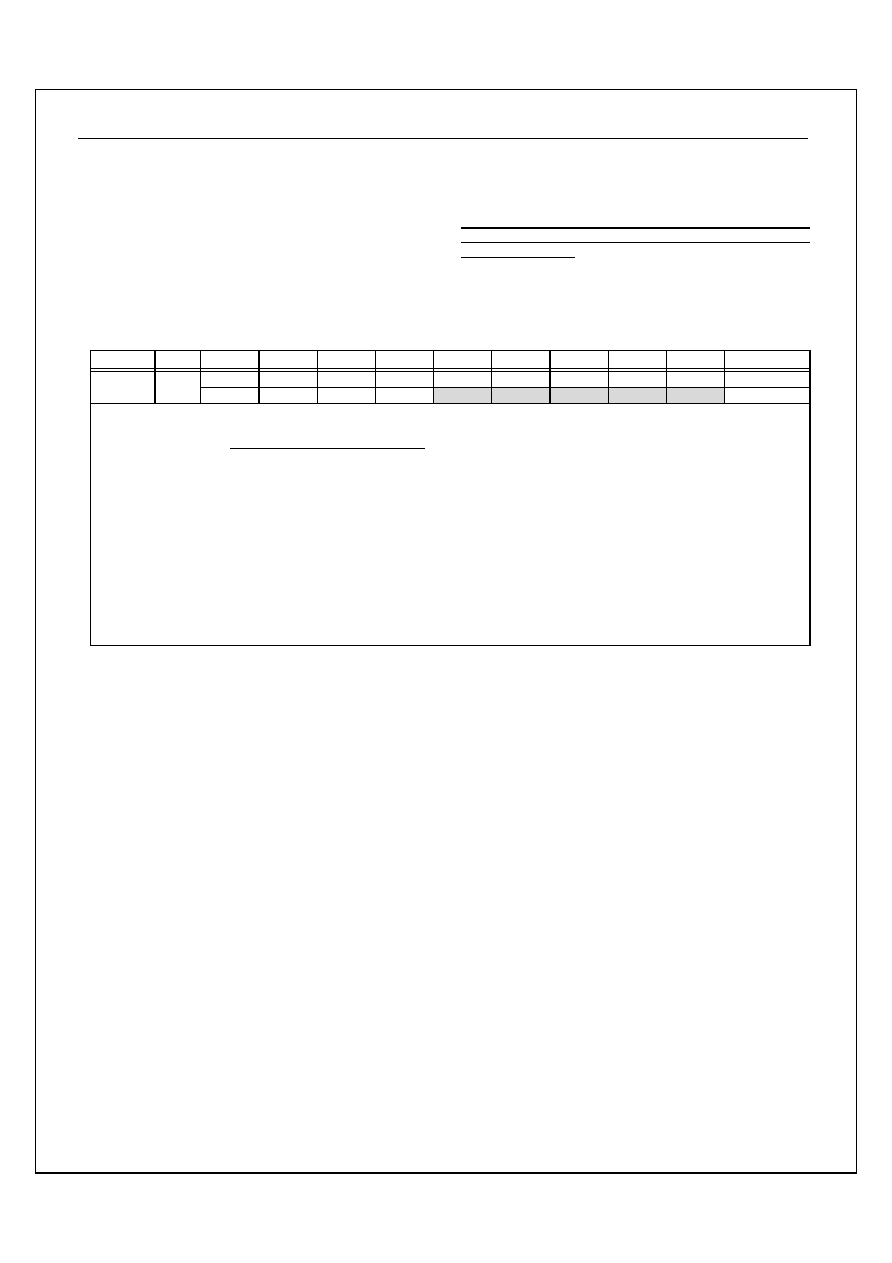
10.4 PORT-D
Port-D only can be used as input. These two pins(PD0,PD1)
are shared with OSCXI and OSCXO by one code option.
The structure of input is different from Port-A/B/C. It has a
latch circuit to keep input value. Once low or high voltages
are inputted, the circuit will latch "0" or "1" respectively. If the
input pin is floating, it keeps the latest value.
FIGURE 10-5: Port-D latch input circuit
Address Name R/W
Bit 7
Bit 6
Bit 5
Bit 4
Bit 3
Bit 2
Bit 1
Bit 0
Default
$03 PD
R/W
-
-
-
-
-
-
PD[1]
PD[0]
- - - - - - 11
Bit 1~0: PD[1~0] :
. If the input pin is floating, it keeps the latest value.
ST2016A
Ver 1.4
20/55
11/11/03
10.5 COMMON-PORT
The COM4~COM7 can be used as LCD drivers or output
ports. In output port mode, COM[7~4] will be map to
COM7~COM4 output ports, which pin assignment will be
decided by Bit 5 of LCTL[5], Please refer to the following
table.
TABLE 10-16: LCD CONTROL REGISTER (LCTL)
Address Name R/W
Bit 7
Bit 6
Bit 5
Bit 4
Bit 3
Bit 2
Bit 1
Bit 0
Default
$03A LCTL W
LPWR BLANK DUTY SCAN
CTR[3] CTR[2] CTR[1] CTR[0] 1000
0000
Bit 5: DUTY : Common output selection bit
1 = 1/8 duty and COM4~COM7 used as LCD Common pins
0 = 1/4 duty and COM4~COM7 used as output pins
TABLE 10-17: COMMON OUTPUT REGISTER (COM)
Address Name R/W
Bit 7
Bit 6
Bit 5
Bit 4
Bit 3
Bit 2
Bit 1
Bit 0
Default
$03B COM R/W COM[7] COM[6] COM[5] COM[4]
-
-
-
-
0000 - - - -
Bit 4: COM[4] : COM4 scan output bit
1 = COM4 output =HIGH
0 = COM4 output =LOW
Bit 5: COM[5] : COM5 scan output bit
1 = COM5 output =HIGH
0 = COM5 output =LOW
Bit 6: COM[6] : COM6 scan output bit
1 = COM6 output =HIGH
0 = COM6 output =LOW
Bit 7: COM[7] : COM7 scan output bit
1 = COM7 output =HIGH
0 = COM7 output =LOW
ST2016A
Ver 1.4
21/55
11/11/03
1
1
1
1
.
.
O
O
s
s
c
c
i
i
l
l
l
l
a
a
t
t
o
o
r
r
ST2016A is with dual-clock system. Programmer can
choose between OSC(RC) and OSCX(32.768k), or both as
clock source through program. The system clock(SYSCK)
also can be switched between OSC and OSCX. The OSC
will be switch with "0" and OSCX will be switch with "1" for
XSEL. Whenever system clock be switch, the warm-up
cycles are occur at the same time. That is confirm SYSCK
really switched when read XSEL bit. LCD driver, Timer1,
Base Timer and PSG can utilize these two clock sources as
well.
TABLE 11-18: SYSTEM CONTROL REGISTER (SYS)
Address Name R/W
Bit 7
Bit 6
Bit 5
Bit 4
Bit 3
Bit 2
Bit 1
Bit 0
Default
$030 SYS R/W XSEL OSTP XSTP XBAK WSKP WAIT
-
-
0000 00- -
Bit 7: XSEL : System clock select(write) / confirm(read) bit
1 = OSCX
0 = OSC
Bit 6: OSTP : OSC stop control bit
1 = Disable OSC
0 = Enable OSC
Bit 5: XSTP : OSCX stop control bit
1 = Disable OSCX
0 = Enable OSCX
Bit 4: XBAK : OSCX driver heavy load bit
1 = OSCX normal load
0 = OSCX heavy load
Bit 3: WSKP : System warm-up control bit
1 = Warm-up to 16 oscillation cycles
0 = Warm-up to 256 oscillation cycles
Bit 2: WAIT : WAI-0 / WAI-1mode select bit (Refer to POWER DOWN MODE)
1 = WAI instruction causes the chip to enter WAI-1 mode
0 = WAI instruction causes the chip to enter WAI-0 mode
Note:
1. The XSEL(SYS[7]) bit will show which real working mode is when it is read.
FIGURE 11-6: System Clock Diagram
2
IN
OUT
MUX2
IN0
IN1
OUTPUT
SEL
OSC
SYSCK
OSCX
XSEL
Frequency divided by 2
ST2016A
Ver 1.4
22/55
11/11/03
1
1
2
2
.
.
T
T
I
I
M
M
E
E
R
R
/
/
E
E
V
V
E
E
N
N
T
T
C
C
O
O
U
U
N
N
T
T
E
E
R
R
The ST2016A has two timers: Base timer/Timer1, and two
prescalers (PRES and PREW). There are two clock sources
for PRES and one clock source(OSCX) for PREW. Please
refer to the following table:
TABLE 12-19: CLOCK SOURCE (TCLK) FOR PRES
SENT Clock
source(TCLK) MODE
1 INTX
Event
counter
0 SYSCK Timer
TABLE 12-20: SUMMARY FOR TIMER REGISTERS
Address Name R/W
Bit 7
Bit 6
Bit 5
Bit 4
Bit 3
Bit 2
Bit 1
Bit 0
Default
$021 BTM R/W
-
-
-
- BTM[3]
BTM[2] BTM[1] BTM[0] - - - - 0000
R
PRS[7] PRS[6] PRS[5] PRS[4] PRS[3] PRS[2] PRS[1] PRS[0] 0000
0000
$023 PRS
W SRES SENA SENT
-
-
-
-
-
000 - - - - -
$026 T1M R/W
-
-
- T1M[4]
T1M[3]
T1M[2] T1M[1] T1M[0]
- - -0 0000
$027 T1C
R/W T1C[7] T1C[6] T1C[5] T1C[4] T1C[3] T1C[2] T1C[1] T1C[0] 0000
0000
$030 SYS R/W XSEL OSTP XSTP XBAK
WSKP WAIT
-
-
0000 00- -
$03C IREQ R/W
-
- IRBT
IRPT IRT1 -
IRDAC
IRX
- - 11 1-11
$03E IENA R/W
-
- IEBT
IEPT IET1 -
IEDAC
IEX
- - 00 0-00
SYSCK
INTX
SENT
O
SEL
MUX
SRES-PULSE
SENA
CK
ENABLE
CLEAR
OUTPUT
TCLK
PREW
OUTPUT
OSCX/256
OSCX/64
OSCX/16
OSCX/4
CK
RESET
OSCX
RESET
IN0
IN1
TCLK/256
TCLK/32
TCLK/8
TCLK/2
PRES
BASE TIMER
TIMER 1
OSCX/128
OSCX/32
FIGURE 12-7: Prescaler for Timers
ST2016A
Ver 1.4
23/55
11/11/03
12.2 PRES
The prescaler PRES is an 8-bits counter as shown in Figure
11-6. Which provides four clock sources for base timer and
timer1, and it is controlled by register PRS. The instruction
read toward PRS will bring out the content of PRES and the
instruction write toward PRS will reset, enable or select clock
sources for PRES.
When user set external interrupt as the input of PRES for
event counter, combining PRES and Timer1 will get a
16bit-event counter.
TABLE 12-21: PRESCALER CONTROL REGISTER (PRS)
Address Name R/W
Bit 7
Bit 6
Bit 5
Bit 4
Bit 3
Bit 2
Bit 1
Bit 0
Default
R
PRS[7] PRS[6] PRS[5] PRS[4] PRS[3] PRS[2] PRS[1] PRS[0] 0000
0000
$023 PRS
W SRES SENA SENT
-
-
-
-
-
000 - - - - -
READ
Bit 7~0: PRS[7~0] : 1's complement of PRES counter
WRITE
Bit 7: SRES : Prescaler Reset bit
Write "1" to reset the prescaler (PRS[7~0])
Bit 6: SENA : Prescaler enable bit
0 = Disable prescaler counting
1 = Enable prescaler counting
Bit 5: SENT : Clock source(TCLK) selection for prescaller PRES
0 = Clock source from system clock "SYSCK"
1 = Clock source from external events "INTX"
12.3 PREW
The prescaler PREW is an 8-bits counter as shown in Figure
11-6. PREW provides four clock source for base timer and
timer1. It stops counting only if OSCX stops or hardware
reset occurs.
ST2016A
Ver 1.4
24/55
11/11/03
12.4 Base timer
Base timer is an 8-bit up counting timer. When it overflows
from $FF to $00, a timer interrupt request IRBT will be
generated. Please refer to Figure 11-7. :
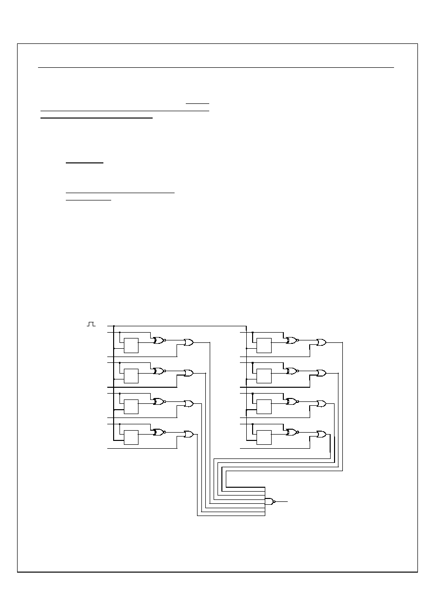
FIGURE 12-8: Structure of Base Timer
IN0
IN1
IN2
IN3
SEL
PRES
BTM[1~0]
MUX4-1
PREW
IN0
IN1
IN2
IN3
SEL
BTM[1~0]
BTM[3]
IN0
IN1
SEL
MUX
8 Bit - UP Counter
CLOCK
IRBT
MUX 4-1
OSCX/256
OSCX/64
OSCX/16
OSCX/4
TCLK/256
TCLK/32
TCLK/8
TCLK/2
OUT
OUT
OUT
12.4.2 Clock source control for Base Timer
Several clock sources can be selected for Base Timer.
Please refer to the following table:
TABLE 12-22: CLOCK SOURCE FOR BASE TIMER
* SENA
BTM[3]
BTM[2] BTM[1] BTM[0] Base
Timer
source
clock
0 0 X
X
X STOP
1 0 X 0 0
TCLK
/
256
1 0 X
0
1
TCLK / 32
1 0 X 1 0
TCLK
/
8
1 0 X
1
1
TCLK / 2
X 1 X
0
0
OSCX / 256
X 1 X
0
1
OSCX / 64
X 1 X
1
0
OSCX / 16
X 1 X
1
1
OSCX / 4
* TCLK will stop when an `0' is written to SENA(PRS[6]).
ST2016A
Ver 1.4
25/55
11/11/03
12.5 Timer 1
The Timer1 is an 8-bit up counter. It can be used as a timer
or an event counter. T1C($27) is a real time read/write
counter. When an overflow from $FF to $00, a timer interrupt
request IRT1 will be generated. Timer1 will stop counting
when system clock stops. Please refer to Figure 11-8.
FIGURE 12-9: Timer1 Structure Diagram
IN0
IN1
IN2
IN3
SEL
PRES
T1M[1~0]
MUX4-1
PREW
IN0
IN1
IN2
IN3
SEL
T1M[1~0]
MUX
8 Bit - UP Counter
CLOCK
IRT1
MUX 4-1
OSCX/256
OSCX/128
OSCX/64
OSCX/32
TCLK/256
TCLK/32
TCLK/8
TCLK/2
OUT
OUT
IN0
IN1
OUT
SEL
D
CK
Q
D Flip-Flop
SYSCK
MUX
T1M[3]
Auto Reload
T1M[4]
TABLE 12-23: TIMER1 COUNTING REGISTER (T1C)
Address Name R/W
Bit 7
Bit 6
Bit 5
Bit 4
Bit 3
Bit 2
Bit 1
Bit 0
Default
$027 T1C R/W T1C[7] T1C[6] T1C[5] T1C[4] T1C[3] T1C[2] T1C[1] T1C[0] 0000
0000
12.5.1.2
Bit 7-0: T1C[7-0] : Timer1 up counter register
ST2016A
Ver 1.4
26/55
11/11/03
12.5.2 Clock source control for Timer1
Several clock source can be chosen from for Timer1. It's
very important that Timer1 can keep counting as long as
SYSCK stays active. Refer to the following table:
TABLE 12-24: CLOCK SOURCE FOR TIMER1
* SENA
T1M[4]
T1M[3]
T1M[2] T1M[1] T1M[0] Clock
source
Auto-Reload
0
X 0 X
X
X STOP
-
1 0 0 X 0 0
TCLK
/
256 No
1 0 0 X 0 1
TCLK
/
32 No
1 0 0 X 1 0
TCLK
/
8 No
1 0 0 X 1 1
TCLK
/
2 No
X 0 1 X
0
0
OSCX / 256
No
X 0 1 X
0
1
OSCX / 128
No
X 0 1 X
1
0
OSCX / 64
No
X 0 1 X
1
1
OSCX / 32
No
1 1 0 X 0 0
TCLK
/
256
Yes
1 1 0 X 0 1
TCLK
/
32 Yes
1 1 0 X 1 0
TCLK
/
8 Yes
1 1 0 X 1 1
TCLK
/
2 Yes
X 1 1 X
0
0
OSCX / 256
Yes
X 1 1 X
0
1
OSCX / 128
Yes
X 1 1 X
1
0
OSCX / 64
Yes
X 1 1 X
1
1
OSCX / 32
Yes
* TCLK would stop when SENA is set to 0.
ST2016A
Ver 1.4
27/55
11/11/03
1
1
3
3
.
.
P
P
S
S
G
G
13.1 Function description
The built-in dual channel Programmable Sound Generator
(PSG) is controlled by registers. Its flexibility makes it useful
in applications such as music synthesis, sound effects
generation, audible alarms and tone signaling. In order to
generate sound effects while allowing the processor to
perform other tasks, the PSG can continue to produce sound
after the initial commands have been given by the CPU. The
structure of PSG was shown in FIGURE 13-11: and the
PSG clock source is shown in FIGURE 13-10: . ST2016A
has three playing modes. First is that both channel0 (CH0)
and channel1 (CH1) output square type tones. Second is
CH0 outputs square tone, and CH1 outputs noise. Third
mode is PWM DAC mode. Sounds of two channels are
mixed into one signal and are outputted in the form of digital
waveform from two pins, PSGOB/PSGO. Therefore one AC
waveform can be performed.
FIGURE 13-10: Clock Source for PSG
RC
OSCX
PSGC[6~4]
IN0
IN1
Output
Select
PSG Selector
PSGCK
PSGC
SYSCK
PSGCK
SYSCK/2
SYSCK/4
SYSCK/8
SYSCK x 2
OSCX
B6 B5 B4
0
0
0
X
X
0
1
1
1
1
1
1
1
0
1
0
0
0
FIGURE 13-11: Program Sound Generator
Enable Output
Enable
LOAD
Output
MUX2
IN0
IN1
OUTPUT
SEL
MUX2
IN0
IN1
OUTPUT
SEL
MUX2
IN0
IN1
OUTPUT
SEL
MIXER
CH1
Output
Vol_CH1
DACE
C1TEN
C1Tone
C1out
DACE
PSGC[2]
C1NEN
C1Noise
PSGC[3]
PSGOB
C1out
VOL[1~0]
PSGO
BD
BDB
DACE
From DAC Generator
Channel 1 Tone
Channel 1 Noise
Preload Data Before First Count
ST2016A
Ver 1.4
28/55
11/11/03
13.2 SUMMARY FOR PSG REGISTERS
Address Name R/W Bit 7
Bit 6
Bit 5
Bit 4
Bit 3
Bit 2
Bit 1
Bit 0
Default
$010 PSG0L R/W PSG0[7] PSG0[6] PSG0[5] PSG0[4] PSG0[3] PSG0[2] PSG0[1] PSG0[0] 0000 0000
$011 PSG0H R/W
-
-
-
-
PSG0[11] PSG0[10]
PSG0[9] PSG0[8] - - - - 0000
$012 PSG1L R/W PSG1[7] PSG1[6] PSG1[5] PSG1[4] PSG1[3] PSG1[2] PSG1[1] PSG1[0] 0000 0000
$013 PSG1H R/W
-
-
-
-
PSG1[11] PSG1[10]
PSG1[9] PSG1[8] - - - - 0000
$015 PSGC2 R/W
-
-
-
-
PSGOD PSGOBD PSGOE PSGOBE - - - - 1111
R/W
-
PCK[2]
PCK[1]
PCK[0]
PRBS
C1EN
C0EN DACE=0 - 000 0000
$016 PSGC
R/W
-
PCK[2]
PCK[1]
PCK[0] DMD[1] DMD[0]
INH
DACE=1 - 000 0000
$017 VOL R/W VOL1[3] VOL1[2] VOL1[1] VOL1[0] VOL0[3] VOL0[2] VOL0[1] VOL0[0]
0000
0000
TABLE 13-25: CONTROL REGISTER FOR PSG OUTPUT (PSGC2)
Address Name R/W
Bit 7
Bit 6
Bit 5
Bit 4
Bit 3
Bit 2
Bit 1
Bit 0
Default
$015 PSGC2 R/W
-
-
-
-
PSGOD PSGOBD PSGOE PSGOBE - - - - 1111
Bit 3: PSGOD : Data bit if PSGO is used as normal output pin.
1 = PSGO is output High.
0 = PSGO is output Low
Bit 2: PSGOBD : Data bit if PSGOB is used as normal output pin.
1 = PSGOB is output High.
0 = PSGOB is output Low
Bit 1: PSGOE : PSG output enable bit
1 = PSGO is PSG data output pin.
0 = PSGO is normal output pin
Bit 0: PSGOBE : PSG inverse signal output enable bit
1 = PSGOB is PSG inverse data output pin.
0 = PSGOB is normal output pin
TABLE 13-26: CONTROL REGISTER FOR PSG VOLUME (VOL)
Address Name R/W
Bit 7
Bit 6
Bit 5
Bit 4
Bit 3
Bit 2
Bit 1
Bit 0
Default
$017 VOL R/W VOL1[3] VOL1[2] VOL1[1] VOL1[0] VOL0[3] VOL0[2] VOL0[1] VOL0[0] 0000 0000
Bit 3~0: VOL0[3~0] : PSG volume control bit
0000 = No sound output
0001 = 1/16 volume (PSGCK must >= 320K Hz)
0010 = 2/16 volume
:
1110 = 15/16 volume
1111 = Maximum volume (PSGCK must >= 20K Hz)
Bit 7~4: VOL1[3~0] : PSG volume control bit
0000 = No sound output
0001 = 1/16 volume (PSGCK must >= 320K Hz)
0010 = 2/16 volume
:
1110 = 15/16 volume
1111 = Maximum volume (PSGCK must >= 20K Hz)
Only use Channel-0 and VOL=0FFHvolume is maximum.
ST2016A
Ver 1.4
29/55
11/11/03
13.3 Tone Generator
The tone frequency is decided by PSGCK and 12-bit
programmable divider (PSG0[11~0]) and (PSG1[11~0])
Please refert Figure12-11.
FIGURE 13-12: Channel0 PSG Tone Counter
12 Bit Auto-reload Up Counter
Tone out
OUTPUT
PSG0[11~8]
PSG0[7~0]
LOAD
C0EN
PSGCK
C0[11~8]
C0[7~0]
Latch
Enable
Frequency of Channel 0 Tone = PSGCK/(1000H-PSG0[11~0])/2
CLOCK
Channel 0
FIGURE 13-13: Channel1 PSG Tone Counter
12 Bit Auto-reload Up Counter
Tone out
OUTPUT
PSG1[11~8]
PSG1[7~0]
LOAD
C1EN
PSGCK
C1[11~8]
C1[7~0]
Latch
Enable
Frequency of Channel 1 Tone = PSGCK/(1000H-PSG1[11~0])/2
CLOCK
Channel 1

ST2016A
Ver 1.4
30/55
11/11/03
13.4 PSG Tone programming
To program tone generator, Tone or DAC function is defined
by DACE, writing to C1EN will enable tone generator when
PSG is in tone function. Noise or tone function is selected by
PRBS.
TABLE 13-27: PSG CONTROL REGISTER (PSGC)
Address Name R/W
Bit 7
Bit 6
Bit 5
Bit 4
Bit 3
Bit 2
Bit 1
Bit 0
Default
R/W
-
PCK[2] PCK[1] PCK[0] PRBS C1EN C0EN DACE=0
-
000
0000
$016 PSGC
R/W
-
PCK[2] PCK[1] PCK[0] DMD[1] DMD[0]
INH
DACE=1 - 000 0000
Bit 0: DACE : Tone(Noise) or DAC Generator selection bit
1 = PSG is used as the DAC generator
0 = PSG is used as the Tone(Noise) generator
Bit 1: C0EN : PSG Channel-0(Tone) enable bit
1 = PSG0 enable
0 = PSG0 disable
Bit 2: C1EN : PSG Channel-1(Tone or Noise) enable bit
1 = PSG1 (Tone or Noise) enable
0 = PSG 1(Tone or Noise) disable
Bit 3: PRBS : Tone or Noise generator selection bit
1 = Noise generator
0 = Tone generator
Bit 6~4: PCK[2~0] : clock source(PSGCK) selection for PSG and DAC
000 = SYSCK
X01 = SYSCK / 2
X10 = SYSCK / 4
011 = SYSCK / 8
100 = SYSCK * 2
111 = OSCX
ST2016A
Ver 1.4
31/55
11/11/03
13.5 Noise Generator Control
Noise generator is shown in Figure 12-12., which base
frequency is controlled by PSG1L[5~0].
FIGURE 13-14: Noise Generator Diagram
PSG1L[5~0]
PSGCK
Noise Prescaler
C1N[5~0]
CLOCK
OUTPUT
NCK
CLOCK
OUTPUT
16-Stage White Noise Generator
Noise out
NCK Frequency = PSGCK/(40H-PSG1L[5~0])
13.6 PSG Noise programming
To program noise generator, Noise or DAC function is
defined by DACE. Writing a "1" to C1EN will enable noise
generator when PSG is in noise mode.
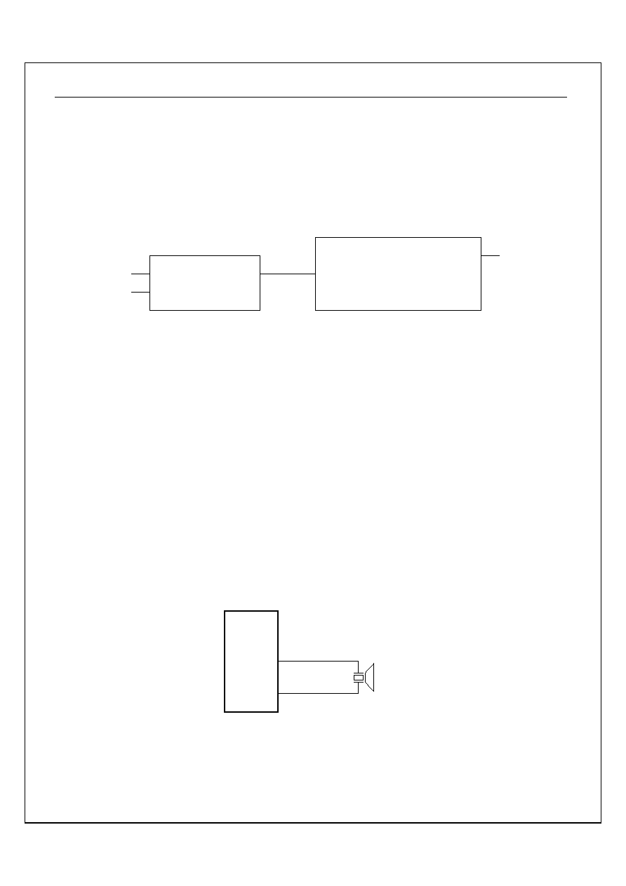
13.7 PSG Applicaion Circuit
Sounds of two channels are modulated by PSGCK and
combine together into one AC signal. Then it outputs on
PSGOB and PSGO. Positive part of the AC signal is output
from PSGO while the negative part is from PSGOB.
FIGURE 13-15: PSG application circuit
P S GO B
S T2016
Buzze r
P S G O
ST2016A
Ver 1.4
32/55
11/11/03
1
1
4
4
.
.
D
D
i
i
g
g
i
i
t
t
a
a
l
l
D
D
A
A
C
C
A built-in digital DAC is for analog sampling data or voice
signals. The structure of DAC is shown in Figure 13-13.
There is an interrupt signal from DAC to CPU whenever DAC
data update is needed and the same signal will decide the
sampling rate of voice. In DAC mode, the OSC can't less 4 M
Hz.
TABLE 14-28: SUMMARY FOR DAC REGISTERS
Address Name R/W Bit 7
Bit 6
Bit 5
Bit 4
Bit 3
Bit 2
Bit 1
Bit 0
Default
$012 PSG1L R/W PSG1[7] PSG1[6] PSG1[5] PSG1[4] PSG1[3] PSG1[2] PSG1[1] PSG1[0] 0000 0000
$013 PSG1H R/W
-
-
-
-
PSG1[11] PSG1[10]
PSG1[9] PSG1[8] - - - - 0000
$014 DAC R/W DAC[7] DAC[6] DAC[5] DAC[4] DAC[3] DAC[2] DAC[1] DAC[0] 0000
0000
$015 PSGC2 R/W
-
-
-
-
PSGOD PSGOBD PSGOE PSGOBE - - - - 1111
R/W
-
PCK[2]
PCK[1]
PCK[0]
PRBS
C1EN C0EN
DACE=0 - 000 0000
$016 PSGC
R/W
-
PCK[2]
PCK[1]
PCK[0] DMD[1] DMD[0]
INH
DACE=1 - 000 0000
TABLE 14-29: DAC DATA REGISTER (DAC)
Address Name R/W
Bit 7
Bit 6
Bit 5
Bit 4
Bit 3
Bit 2
Bit 1
Bit 0
Default
$014 DAC R/W DAC[7] DAC[6] DAC[5] DAC[4] DAC[3] DAC[2] DAC[1] DAC[0] 0000
0000
Bit 7~0: DAC[7~0] : DAC output data
Note: For Single-Pin Single Ended mode, the effective output resolution is 7 bit.
ST2016A
Ver 1.4
33/55
11/11/03
TABLE 14-30: DAC CONTROL REGISTER (PSGC)
Address Name R/W
Bit 7
Bit 6
Bit 5
Bit 4
Bit 3
Bit 2
Bit 1
Bit 0
Default
R/W
-
PCK[2] PCK[1] PCK[0]
PRBS
C1EN
-
DACE=0 - 000 00-0
$016 PSGC
R/W
-
PCK[2] PCK[1] PCK[0] DMD[1] DMD[0] INH DACE=1
-
000
0000
Bit 0: DACE : PSG play as Tone(Noise) or DAC Generator selection bit
1 = PSG is used as DAC Generator
0 = PSG is used as Tone(Noise) Generator
Bit 1: INH : DAC output inhibit control bit
1 = DAC output inhibit
0 = DAC output enable
Bit 3~2: DMD[1~0] : DAC output mode selection
00 = Single-Pin mode : 7 bit resolution
01 = Two-Pin Two Ended mode : 8 bit resolution
10 = Reserved
11 = Two-Pin Push Pull mode : 8 bit resolution
Bit 6~4: PCK[2~0] : PSGCK selection for PSG and DAC
000 = SYSCK / 2
X01 = SYSCK / 4
X10 = SYSCK / 8
011 = SYSCK / 16
100 = SYSCK *
111 = OSCX
* In DAC mode, PSGCK must select SYSCK.
ST2016A
Ver 1.4
34/55
11/11/03
14.2 Sampling Rate Control
The sample rate is controlled by PSG1L and PSG1H.
PSG1[11~7] controls sample rate/post scaling and PSG1[6]
must set `0' and PSG1[5~0] must set `1'. The input clock
source is controlled by PCK[2~0]. The block diagram is
shown as the following:
FIGURE 14-16: DAC Generator Diagram
Sample Rate Generator
CK_IN
Enable
Output
PSG[11~0]
PWM Generator
DAC[7~0]
Enable
Fs
PO
POB
Reload_DAC
INH
DAC[7~0]
DMD[0]
DMD[1]
BD
PSG[11~0]
PSGCK
Fs
BDB
DACE
Reload_DAC
DMD[1]
DMD[0]
FIGURE 14-17: Clock Source for DAC
RC
OSCX
PSGC[6~4]
IN0
IN1
Output
Select
PSG Selector
PSGCK
PSGC
SYSCK
PSGCK
SYSCK/2
SYSCK/4
SYSCK/8
SYSCK x 2
OSCX
B6 B5 B4
0
0
0
X
X
0
1
1
1
1
1
1
1
0
1
0
0
0
TABLE 14-31: DAC Sample Rate Description (RC
OSC
= 2MHz)
DAC interrupt frequency
PSGC b6, b5, b4
PSG1H, PSG1L
8K 100
00001111,
00111111
16K 100
00001111,
10111111
ST2016A
Ver 1.4
35/55
11/11/03
14.3 PWM DAC Mode Select
The PWM DAC generator has three modes, Single-pin
mode, Two-pin two ended mode and Two-pin push pull
mode. They are depended on the application used. The DAC
mode is controlled by DMD[1~0]. (TABLE 13-31)
14.3.1 Single-Pin Mode (Accurate to 7 bits)
Single-pin mode is designed for use with a single-transistor
amplifier. It has 7 bits of resolution. The duty cycle of the
PSGO is proportional to the output value. If the output value
is 0, the duty cycle is 50%. As the output value increases
from 0 to 63, the duty cycle goes from being high 50% of the
time up to 100% high. As the value goes from 0 to -64, the
duty cycle decreases from 50% high to 0%. PSGOB is
inverse of PSGO's waveform. Figure 13-15 shows the
PSGO wave-forms.
FIGURE 14-18: Single-Pin PWM DAC Wave-form
DAC = 0
64
64
DAC = 32
DAC = -32
DAC = X
96
32
32
96
64+X
64-X
High
Low
PSGO
FIGURE 14-19: Single-Pin Application Circuit
P S GO
330 ohm
8050
ST2016
SPK
ST2016A
Ver 1.4
36/55
11/11/03
14.3.2 Two-Pin Two Ended mode (Accurate to 8 bits)
Two-Pin Two Ended mode is designed for use with a single
transistor amplifier. It requires two pins that PSGOB and
PSGO. When the DAC value is positive, PSGO goes high
with a duty cycle proportional to the output value, while
PSGOB stays high. When the DAC value is negative,
PSGOB goes low with a duty cycle proportional to the output
value, while PSGO stays low. This mode offers a resolution
of 8 bits.
Figure 13-17 shows examples of DAC output waveforms
with different output values. Each pulse of the DAC is divided
into 128 segments per sample period. For a positive output
value x=0 to 127, PSGO goes high for X segments while
PSGOB stays high. For a negative output value x=0 to -127,
PSGOB goes low for |X| segments while PSGO stays low.
FIGURE 14-20: Two-Pin Two Ended PWM DAC Wave-form
FIGURE 14-21: Two-Pin Two Ended mode Application Circuit
High
Low
PSGOB
DAC = X
Where X=0 to 127
DAC = 96
High
Low
PSGO
X
128-X
DAC = 32
DAC = 127
127
1
96
32
32
96
High
Low
PSGOB
DAC = X
Where X=0 to -128
DAC = 0
High
Low
PSGO
|X|
128+X
DAC = -48
DAC = -128
48
80
P S G OB
680
8050
ST2016
PSGO
SPK
680
1K
.1u
1u
2.2K
Output 1:ON
0:OFF

ST2016A
Ver 1.4
37/55
11/11/03
14.3.3 Two-Pin Push Pull mode (Accurate to 8 bits)
Two-Pin Push Pull mode is designed for buzzer. It requires
two pins that PSGOB and PSGO. When the DAC value is 0,
both pins are low. When the DAC value is positive, PSGO
goes high with a duty cycle proportional to the output value,
while PSGOB stays low. When the DAC value is negative,
PSGOB goes high with a duty cycle proportional to the
output value, while PSGO stays low. This mode offers a
resolution of 8 bits.
Figure 13-19 shows examples of DAC output waveforms
with different output values. Each pulse of the DAC is divided
into 128 segments per sample period. For a positive output
value x=0 to 127, PSGO goes high for X segments while
PSGOB stays low. For a negative output value x=0 to -127,
PSGOB goes high for |X| segments while PSGO stays low.
FIGURE 14-22: Two-Pin Push Pull Mode Waveform
FIGURE 14-23: Two-Pin Push Pull Application Circuit
High
Low
PSGOB
DAC = X
Where X=0 to 127
DAC = 96
High
Low
PSGO
X
128-X
DAC = 32
DAC = 127
127
1
96
32
32
96
High
Low
PSG0
DAC = X
Where X=0 to -128
DAC = 0
High
Low
PSG1
|X|
128+X
DAC = -48
DAC = -128
48
80
P S G O B
ST2016
Buzzer
PSGO
ST2016A
Ver 1.4
38/55
11/11/03
1
1
5
5
.
.
L
L
C
C
D
D
The ST2016A can drive up to 320 dots of LCD panel directly.
The LCD driver can control by 1/4 duty(160 dots) and 1/8
duty (320 dots). LCD block include display RAM ($200~
$227) for storing the display data, 40-segment output pins
(SEG0~SEG39), 8-common output pins (COM0~COM7).
All LCD RAM are random after power on reset. The bias
voltage circuits of the LCD display is built-in and no external
resistor is needs.
FIGURE 15-24: Clock source of LCD
SYSCK
INTX
SENT
O
SEL
MUX
SRES-PULSE
SENA
CK
ENABLE
CLEAR
OUTPUT
TCLK
IN0
IN1
TCLK/64
TCLK/32
TCLK/16
TCLK/8
PRES
MUX4-1
IN0
IN3
IN2
IN1
SEL
OUT
LCK[1~0]
IN0
IN1
OSCX
SEL
LCK[2]
OUT
IN
OUT
:
64
LCD clock
ST2016A
Ver 1.4
39/55
11/11/03
15.2 LCD driver 1/4 duty output
COM0
COM1
COM2
COM3
SEGx
SEGx
All Off
All On
V0
V1
V2
V3
1/4 duty , 1/3 bias LCD signal
V0
V1
V2
V3
V0
V1
V2
V3
V0
V1
V2
V3
Phase1
Phase2
V0
V1
V2
V3
V0
V1
V2
V3
COM3
COM2
COM1
COM0
SEGx+1
SEGx
Example
SEGx
SEGx
V0
V1
V2
V3
V0
V1
V2
V3
Phase1
Phase2
ST2016A
Ver 1.4
40/55
11/11/03
15.3 LCD driver 1/8 duty output
COM0
COM1
SEGx
SEGx
All Off
All On
V0
V1
V2
V3
1/8 duty , 1/4 bias LCD signal
Example
V4
V0
V1
V2
V3
V4
V0
V1
V2
V3
V4
COM7
V0
V1
V2
V3
V4
V0
V1
V2
V3
V4
COM0
COM1
COM2
COM3
COM4
COM5
COM6
COM7
SEGx
SEGx+1
SEGx
SEGx+1
V0
V1
V2
V3
V4
V0
V1
V2
V3
V4
Phase1
Phase2
Phase1
Phase2
ST2016A
Ver 1.4
41/55
11/11/03
15.4 LCD Control Register
15.4.1.1
LCD Segment Number Selection Register (LSEL)
Address Name R/W
Bit 7
Bit 6
Bit 5
Bit 4
Bit 3
Bit 2
Bit 1
Bit 0
Default
$039 LSEL R/W
LSEL[7]
-
-
LSEL[4] LSEL[3] LSEL[2] LSEL[1] LSEL[0]
0 - -0 0000
Bit 7 LSEL[7] :
1 = PA[7~4] will use as LCD segment driver SEG[3~0]
0 = PA[7~4] will be general purpose I/O
Bit 4~0: LSEL[4~0] : LCD segment number selection
Pad Definition
LSEL[4:0] PAD
PAD
PAD
PAD
PAD
PAD
PAD
PAD
PAD
PAD
PAD
PAD
PAD
PAD
PAD
PAD
0 xxxx
PC0
PC1
PC2
PC3
PC4
PC5
PC6
PC7
PB0
PB1
PB2
PB3
PB4
PB5
PB6
PB7
1 0000
SEG24 PC1
PC2
PC3
PC4
PC5
PC6
PC7
PB0
PB1
PB2
PB3
PB4
PB5
PB6
PB7
1 0001
SEG24 SEG25 PC2
PC3
PC4
PC5
PC6
PC7
PB0
PB1
PB2
PB3
PB4
PB5
PB6
PB7
1 0010 SEG24 SEG25 SEG26 PC3
PC4
PC5
PC6
PC7
PB0
PB1
PB2
PB3
PB4
PB5
PB6
PB7
1 0011 SEG24 SEG25 SEG26 SEG27 PC4
PC5
PC6
PC7
PB0
PB1
PB2
PB3
PB4
PB5
PB6
PB7
1 0100 SEG24 SEG25 SEG26 SEG27 SEG28 PC5
PC6
PC7
PB0
PB1
PB2
PB3
PB4
PB5
PB6
PB7
1 0101 SEG24 SEG25 SEG26 SEG27 SEG28 SEG29 PC6
PC7
PB0
PB1
PB2
PB3
PB4
PB5
PB6
PB7
1 0110 SEG24 SEG25 SEG26 SEG27 SEG28 SEG29 SEG30 PC7
PB0
PB1
PB2
PB3
PB4
PB5
PB6
PB7
1 0111 SEG24 SEG25 SEG26 SEG27 SEG28 SEG29 SEG30 SEG31 PB0
PB1
PB2
PB3
PB4
PB5
PB6
PB7
1 1000 SEG24 SEG25 SEG26 SEG27 SEG28 SEG29 SEG30 SEG31 SEG32 PB1
PB2
PB3
PB4
PB5
PB6
PB7
1 1001 SEG24 SEG25 SEG26 SEG27 SEG28 SEG29 SEG30 SEG31 SEG32 SEG33 PB2
PB3
PB4
PB5
PB6
PB7
1 1010 SEG24 SEG25 SEG26 SEG27 SEG28 SEG29 SEG30 SEG31 SEG32 SEG33 SEG34 PB3
PB4
PB5
PB6
PB7
1 1011 SEG24 SEG25 SEG26 SEG27 SEG28 SEG29 SEG30 SEG31 SEG32 SEG33 SEG34 SEG35 PB4
PB5
PB6
PB7
1 1100 SEG24 SEG25 SEG26 SEG27 SEG28 SEG29 SEG30 SEG31 SEG32 SEG33 SEG34 SEG35 SEG36 PB5
PB6
PB7
1 1101 SEG24 SEG25 SEG26 SEG27 SEG28 SEG29 SEG30 SEG31 SEG32 SEG33 SEG34 SEG35 SEG36 SEG37 PB6
PB7
1 1110 SEG24 SEG25 SEG26 SEG27 SEG28 SEG29 SEG30 SEG31 SEG32 SEG33 SEG34 SEG35 SEG36 SEG37 SEG38 PB7
1 1111 SEG24 SEG25 SEG26 SEG27 SEG28 SEG29 SEG30 SEG31 SEG32 SEG33 SEG34 SEG35 SEG36 SEG37 SEG38 SEG39
ST2016A
Ver 1.4
42/55
11/11/03
15.5 LCD control register
TABLE 15-32: LCD CONTROL REGISTERS
Address Name R/W
Bit 7
Bit 6
Bit 5
Bit 4
Bit 3
Bit 2
Bit 1
Bit 0
Default
$020 LCK R/W
DRV[4] DRV[3] DRV[2] DRV[1] DRV[0] LCK[2] LCK[1] LCK[0] 0000
0000
$023 PRS R/W SRES SENA SENT
-
-
-
-
-
000 - - - - -
$03A LCTL W LPWR BLANK DUTY SCAN CTR[3] CTR[2] CTR[1] CTR[0] 1000
0000
TABLE 15-33: LCD FREQUENCY REGISTER (LCK)
Address Name R/W
Bit 7
Bit 6
Bit 5
Bit 4
Bit 3
Bit 2
Bit 1
Bit 0
Default
$020 LCK R/W
DRV[4]
DRV[3]
DRV[2] DRV[1] DRV[0] LCK[2] LCK[1] LCK[0] 0000
0000
Bit 7~3: DRV[4~0] : LCD driving strength control.
*** Measure Condition: Vdd=3V, LCD frame rate=64Hz, OSCX: normal load , in WAI1.
Bit 2~0: LCK[2~0] : LCD clock source
LCK[2:0]
Frame Rate
000
OSC / 131072 ( 4MHz / 131072 = 30.5Hz )
001
OSC / 65536 ( 4MHz / 65536 = 61.0Hz )
010
OSC / 32768 ( 4MHz / 32768 = 122.1Hz )
011
OSC / 16384 ( 4MHz / 16384 = 244.1Hz )
1XX
OSCX / 512 ( 32768 / 512 = 64Hz )
LCK[7:3] Driving
strength
1/4 Duty
consumption
(uA)
1/8 Duty
consumption
(uA)
LCK[7:3] Driving strength
1/4 Duty
consumption
(uA)
1/8 Duty
consumption
(uA)
00000
Level 31(max.)
65.38
49.22
10000
Level 15
36.99
27.81
00001
Level 30
63.63
47.88
10001
Level 14
35.2
26.45
00010
Level 29
61.81
46.54
10010
Level 13
33.42
25.13
00011
Level 28
60.05
45.2
10011
Level 12
31.65
23.8
00100 Level
27 57.93 43.88 10100 Level
11 29.88 22.46
00101
Level 26
58.26
42.53
10101
Level 10
28.12
21.13
00110
Level 25
54.73
41.2
10110
Level 9
26.31
19.78
00111
Level 24
52.94
39.85
10111
Level 8
24.54
18.44
01000
Level 23
51.16
38.5
11000
Level 7
22.75
17.1
01001
Level 22
49.39
37.18
11001
Level 6
20.98
15.79
01010
Level 21
47.63
35.82
11010
Level 5
19.2
14.42
01011
Level 20
45.85
34.5
11011
Level 4
17.43
13.11
01100
Level 19
44.07
33.16
11100
Level 3
15.63
11.75
01101
Level 18
42.28
31.81
11101
Level 2
13.84
10.4
01110
Level 17
40.53
30.5
11110
Level 1
12.02
9.07
01111
Level 16
38.75
29.15
11111
Level 0(mini.)
10.23
7.71
* SENA must switch "1". ( refer to FIGURE 14-21 )
ST2016A
Ver 1.4
43/55
11/11/03
TABLE 15-34: LCD CONTROL REGISTER (LCTL)
Address Name R/W
Bit 7
Bit 6
Bit 5
Bit 4
Bit 3
Bit 2
Bit 1
Bit 0
Default
$03A LCTL W LPWR BLANK DUTY SCAN CTR[3] CTR[2] CTR[1] CTR[0]
1000
0000
Bit 7: LPWR : LCD power ON/OFF bit
1 = LCD power OFF
0 = LCD power ON
Bit 6: BLANK : LCD display ON/OFF bit
1 = Disable LCD display (Common line is still scanning)
0 = Enable LCD display
Bit 5: DUTY : LCD duty control bit
1 = 1/8 duty (1/4 bias)
0 = 1/4 duty (1/3 bias)
Bit 4: SCAN : LCD segment keyboard scan function
1 = Enable LCD keyboard awaking pulse in LCD waveforms
0 = Disable LCD keyboard awaking pulse
Bit 2~1: CTR[3~0] : LCD Contrast Control
Frame Rate = 64Hz (DUTY=1/8 , DUTY=1/4)
0000 = contrast level 16 (maximum)
0001 = contrast level 15
0010 = contrast level 14
0011 = contrast level 13
0100 = contrast level 12
0101 = contrast level 11
0110 = contrast level 10
0111 = contrast level 9
1000 = contrast level 8
1001 = contrast level 7
1010 = contrast level 6
1011 = contrast level 5
1100 = contrast level 4
1101 = contrast level 3
1110 = contrast level 2
1111 = contrast level 1 (minimum)
ST2016A
Ver 1.4
44/55
11/11/03
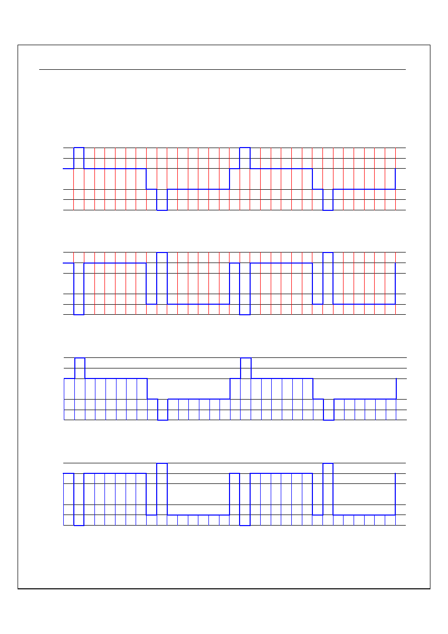
15.6 Keyboard-scan Function on LCD drives
When the LCTL[4] is set to "1", the SCAN function will be
enabled. The LCD waveform will appear Keyboard Awaking
Pulses. These pulses are used as keyboard scan line to
trigger Port-A interrupt if the keys have being pressed.
FIGURE 15-25: LCD Segment Waveform (Without Keyboard Awaking Pulses)
VP
V2
V1
V3
V5
V4
FIGURE 15-26: LCD Common Waveform (Without Keyboard Awaking Pulses)
VP
V2
V1
V3
V5
V4
FIGURE 15-27: LCD Segment Waveform (With Keyboard Awaking Pulses)
V
V
V
VP
P
P
P
V
V
V
V2222
V
V
V
V1111
V
V
V
V3333
V
V
V
V5555
V
V
V
V4444
FIGURE 15-28: LCD Common Waveform (With Keyboard Awaking Pulses)
VP
V2
V1
V3
V5
V4
ST2016A
Ver 1.4
45/55
11/11/03
15.6.2 Keyboard-scan
Function Example:
a. Keyboard : 64Keys (8x8)
b. Return Lines : Port-A
c. Scan Lines : Port-B
.
.
.
INITIAL_Port_And_LCD
SMB4 <LCTL
;;Enable Keyboard Awaking Pulses Waveform
LDA #000
11111B
;;Set all shared pins to be segments
STA <LSEL
STZ
<PCA
;;Set Port-A as Inputs for Return Line
LDA #FFH
STA <PA
;;Port-A
Pull-High
STA
<PCB
;;Set Port-B as Outputs for Scan Line
LDA #11000000B
STA
<PMCR
;;Enable Pull up & Debounce
LDA #00010000B
STA <IENA
;;Enable
Port-A
Interrupt
LDA
<PA
;;Keep Port-A last state
LDA #$FF
STA
<PAK
;;Port-A used as keyboard return line
STZ
<IREQ
;;Reset Interrupt Request Register
.
CLI
.
.
I
I
I
Innnniiiittttiiiiaaaallll IIII////O
O
O
O
(
(
(
(E
E
E
E nnnnaaaabbbblllleeee D
D
D
Deeeebbbboooouuuunnnncccceeee &
&
&
&
P
P
P
P oooorrrr tttt----A
A
A
A sssseeeetttt ttttoooo rrrr eeeettttuuuurrrr nnnn lllliiiinnnneeee ))))
C
C
C
C L
L
L
L IIII
I
I
I
I nnnniiiittttiiiiaaaallll IIIInnnntttteeeerrrr rrrr uuuupppptttt////L
L
L
L C
C
C
C D
D
D
D
.
.
.
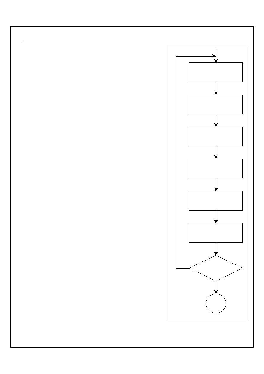
ST2016A
Ver 1.4
46/55
11/11/03
Interrupt-Subroutine
Port_ISR
PHA
PHX
LDA
#11111110B
;;Initial scanning value for Port-B
STA <ScanValue
?Scan_PB
STA <PB
STZ
<PAK
;; Port-A used as normal I/O
RMB3 <LSEL
;;Change segments to be Port-B
LDX #$FF
:
:
wait 12us ;
;Wait for return line to be stable
:
:
LDA <PA
SMB3 <LSEL
;;Change Port-B to be segments
STX
<PAK
;;Port-A used as keyboard return line
JSR
Store-Key-Data ;;This subroutine should be defined by user
ROL
<Scanvalue
;;Shift scanning value left
LDA <Scanvalue
BCS ?Scan_PB
.
.
PLX
PLA
RTI
E
E
E
E nnnn dddd ooooffff S
S
S
Sccccaaaannnn nnnn iiiinnnn gggg????
R
R
R
R T
T
T
T IIII
R
R
R
R eeeeaaaa dddd P
P
P
P oooorrrr tttt----A
A
A
A
S
S
S
Seeeetttt P
P
P
P oooorrrr tttt----A
A
A
A ttttoooo N
N
N
Noooorrrr m
m
m
m aaaallll IIII ////O
O
O
O
&
&
&
& W
W
W
W aaaaiiiitttt ttttoooo S
S
S
Sttttaaaa bbbb lllleeee
T
T
T
T uuuu rrrr nnnn O
O
O
O N
N
N
N P
P
P
P oooorrrr tttt----B
B
B
B
O
O
O
O uuuu ttttpppp uuuu tttt S
S
S
Sccccaaaannnn V
V
V
Vaaaa lllluuuu eeee oooonnnn
S
S
S
Sccccaaaannnn L
L
L
L iiiinnnn eeeessss
T
T
T
T uuuu rrrr nnnn O
O
O
O F
F
F
F F
F
F
F P
P
P
P oooorrrr tttt----B
B
B
B &
&
&
&
P
P
P
P oooorrrr tttt----A
A
A
A sssseeeetttt ttttoooo rrrr eeeettttuuuu rrrr nnnn lllliiiinnnn eeee
S
S
S
Sttttoooorrrr eeee K
K
K
K eeeeyyyy D
D
D
Daaaattttaaaa
Y
Y
Y
Yeeeessss
N
N
N
Noooo
TABLE 1-2:
ST2016A
Ver 1.4
47/55
11/11/03
15.7 LCD RAM map
The LCD RAM map is shown as following:
TABLE 15-35: LCD RAM MAPPING
SEG ADDRESS COM0 COM1 COM2 COM3 COM4 COM5 COM6 COM7
0
200H
Bit 0
Bit 1
Bit 2
Bit 3
Bit 4
Bit 5
Bit 6
Bit 7
1
201H
Bit 0
Bit 1
Bit 2
Bit 3
Bit 4
Bit 5
Bit 6
Bit 7
2
202H
Bit 0
Bit 1
Bit 2
Bit 3
Bit 4
Bit 5
Bit 6
Bit 7
3
203H
Bit 0
Bit 1
Bit 2
Bit 3
Bit 4
Bit 5
Bit 6
Bit 7
4
204H
Bit 0
Bit 1
Bit 2
Bit 3
Bit 4
Bit 5
Bit 6
Bit 7
5
205H
Bit 0
Bit 1
Bit 2
Bit 3
Bit 4
Bit 5
Bit 6
Bit 7
6
206H
Bit 0
Bit 1
Bit 2
Bit 3
Bit 4
Bit 5
Bit 6
Bit 7
7
207H
Bit 0
Bit 1
Bit 2
Bit 3
Bit 4
Bit 5
Bit 6
Bit 7
8
208H
Bit 0
Bit 1
Bit 2
Bit 3
Bit 4
Bit 5
Bit 6
Bit 7
9
209H
Bit 0
Bit 1
Bit 2
Bit 3
Bit 4
Bit 5
Bit 6
Bit 7
10
20AH
Bit 0
Bit 1
Bit 2
Bit 3
Bit 4
Bit 5
Bit 6
Bit 7
11
20BH
Bit 0
Bit 1
Bit 2
Bit 3
Bit 4
Bit 5
Bit 6
Bit 7
12
20CH
Bit 0
Bit 1
Bit 2
Bit 3
Bit 4
Bit 5
Bit 6
Bit 7
13
20DH
Bit 0
Bit 1
Bit 2
Bit 3
Bit 4
Bit 5
Bit 6
Bit 7
14
20EH
Bit 0
Bit 1
Bit 2
Bit 3
Bit 4
Bit 5
Bit 6
Bit 7
15
20FH
Bit 0
Bit 1
Bit 2
Bit 3
Bit 4
Bit 5
Bit 6
Bit 7
16
210H
Bit 0
Bit 1
Bit 2
Bit 3
Bit 4
Bit 5
Bit 6
Bit 7
17
211H
Bit 0
Bit 1
Bit 2
Bit 3
Bit 4
Bit 5
Bit 6
Bit 7
18
212H
Bit 0
Bit 1
Bit 2
Bit 3
Bit 4
Bit 5
Bit 6
Bit 7
19
213H
Bit 0
Bit 1
Bit 2
Bit 3
Bit 4
Bit 5
Bit 6
Bit 7
20
214H
Bit 0
Bit 1
Bit 2
Bit 3
Bit 4
Bit 5
Bit 6
Bit 7
21
215H
Bit 0
Bit 1
Bit 2
Bit 3
Bit 4
Bit 5
Bit 6
Bit 7
22
216H
Bit 0
Bit 1
Bit 2
Bit 3
Bit 4
Bit 5
Bit 6
Bit 7
23
217H
Bit 0
Bit 1
Bit 2
Bit 3
Bit 4
Bit 5
Bit 6
Bit 7
24
218H
Bit 0
Bit 1
Bit 2
Bit 3
Bit 4
Bit 5
Bit 6
Bit 7
25
219H
Bit 0
Bit 1
Bit 2
Bit 3
Bit 4
Bit 5
Bit 6
Bit 7
26
21AH
Bit 0
Bit 1
Bit 2
Bit 3
Bit 4
Bit 5
Bit 6
Bit 7
27
21BH
Bit 0
Bit 1
Bit 2
Bit 3
Bit 4
Bit 5
Bit 6
Bit 7
28
21CH
Bit 0
Bit 1
Bit 2
Bit 3
Bit 4
Bit 5
Bit 6
Bit 7
29
21DH
Bit 0
Bit 1
Bit 2
Bit 3
Bit 4
Bit 5
Bit 6
Bit 7
30
21EH
Bit 0
Bit 1
Bit 2
Bit 3
Bit 4
Bit 5
Bit 6
Bit 7
31
21FH
Bit 0
Bit 1
Bit 2
Bit 3
Bit 4
Bit 5
Bit 6
Bit 7
32
220H
Bit 0
Bit 1
Bit 2
Bit 3
Bit 4
Bit 5
Bit 6
Bit 7
33
221H
Bit 0
Bit 1
Bit 2
Bit 3
Bit 4
Bit 5
Bit 6
Bit 7
34
222H
Bit 0
Bit 1
Bit 2
Bit 3
Bit 4
Bit 5
Bit 6
Bit 7
35
223H
Bit 0
Bit 1
Bit 2
Bit 3
Bit 4
Bit 5
Bit 6
Bit 7
36
224H
Bit 0
Bit 1
Bit 2
Bit 3
Bit 4
Bit 5
Bit 6
Bit 7
37
225H
Bit 0
Bit 1
Bit 2
Bit 3
Bit 4
Bit 5
Bit 6
Bit 7
38
226H
Bit 0
Bit 1
Bit 2
Bit 3
Bit 4
Bit 5
Bit 6
Bit 7
39
227H
Bit 0
Bit 1
Bit 2
Bit 3
Bit 4
Bit 5
Bit 6
Bit 7
Note:
1. The LCD RAM address is allocated at page 2 of memory map. Only bit0 ~ bit3 is useful when it is 1/4 duty
mode.
2. The LCD RAM can be write & read as like general purpose RAM.
ST2016A
Ver 1.4
48/55
11/11/03
1
1
6
6
.
.
P
P
o
o
w
w
e
e
r
r
D
D
o
o
w
w
n
n
M
M
o
o
d
d
e
e
The ST2016A has three power down modes: WAI-0, WAI-1
and STP. The instruction WAI will enable mode WAI-0 or
WAI-1, which are controlled by WAIT(SYS[2]). The
instruction WAI (WAI-0 and WAI-1 modes) can be wake-up
by interrupt. However, the instruction of STP can only be
wake-up by hardware reset.
16.1 WAI-0 Mode:
When WAIT is cleared, WAI instruction lets MCU enter
WAI-0 mode. In the mean time, oscillator circuit is be active
and interrupts, timer/counter, and PSG will all be working.
Under such circumstance, CPU stops and the related
instruction execution will stop. All registers, RAM, and I/O
pins will retain their states before the MCU enter standby
mode. WAI-0 mode can be wake-up by reset or interrupt
request. If user disable interrupt(CPU register I='1'), MCU
will still be wake-up but not go into the interrupt service
routine. If interrupt is enabled(CPU register I='0'), the
corresponding interrupt vector will be fetched and interrupt
service routines will executed.
The sample program is showed as followed:
LDA #$00
STA SYS
WAI
; WAI 0 mode
16.2 WAI-1 Mode:
When WAIT is set, WAI instruction let MCU to enter WAI-1
mode. In this mode, the CPU will stop, but PSG,
timer/counter won't stop if the clock source is from OSCX.
The wake-up procedure is the same as the one for WAI-0.
But the warm-up cycles are occur when WAI-1 wake-up.
The sample program is shown as the following:
LDA #$04
STA SYS
WAI
; WAI 1 mode
16.3 STP Mode:
STP instruction will force MCU to enter stop mode. In this
mode, MCU stops, but PSG, timer/counter won't stop if the
clock source is from OSCX. In power-down mode, MCU only
be wake-up by hardware reset, and the warm-up cycles are
occur at the same time.
The sample program is showed as the following:
.
.
STP
.
.
TABLE 16-36: STATUS UNDER POWER DOWN MODE
(SYSCK source from OSC)
Mode Timer0,1 SYSCK
OSC
OSCX
Base
Timer
RAM REG. LCD I/O Wake-up
condition
WAI-0
Retain
Reset, Any interrupt
WAI-1
Stop
Stop
Stop Retain Reset,
Any
interrupt
STP Stop
Stop Stop
Retain
Reset
(SYSCK source from OSCX)
Mode Timer0,1 SYSCK
OSC
OSCX
Base
Timer
RAM REG. LCD I/O Wake-up
condition
WAI-0
Retain
Reset, Any interrupt
WAI-1
Stop
Stop
Retain
Reset, Any interrupt
STP Stop
Stop
Retain
Reset
ST2016A
Ver 1.4
49/55
11/11/03
1
1
7
7
.
.
E
E
l
l
e
e
c
c
t
t
r
r
i
i
c
c
a
a
l
l
C
C
h
h
a
a
r
r
a
a
c
c
t
t
e
e
r
r
i
i
s
s
t
t
i
i
c
c
s
s
DC Supply Voltage ------------------------------ -0.3V to +7.0V
Operating Ambient Temperature ----------- -10
�
C to +60
�
C
Storage Temperature ------------------------- -10
�
C to +125
�
C
17.1 DC Electrical Characteristics
Standard operation conditions: V
DD
= 3.0V, GND = 0V, T
A
=
25
�
C, OSC = 4M Hz, OSCX = 32768 Hz,unless otherwise specified
Parameter
Symbol
Min. Typ. Max. Unit
Condition
Operating Voltage
V
DD
2.4 3 3.6 V
Operating Current
I
OP
870
1300
�
A
All output pins unload, execute NOP instruction,
LCD on
Standby Current 1
I
SB0
0.5 1
�
A
All output pins unload, OSCX off, LCD off
(WAIT1/STOP mode)
Standby Current 2
I
SB1
1.6
2.5
�
A
All output pins unload, OSCX on(normal), LCD off
(WAIT1/STOP mode)
Standby Current 3
I
SB1
3 4.5
�
A
All output pins unload, OSCX on(heavy), LCD off
(WAIT1/STOP mode)
Standby Current 6
I
SB4
85
128
�
A
All output pins unload, OSCX on(normal), LCD off
(WAIT0 mode)
Input High Voltage
V
IH
0.7V
DD
- V
DD
+ 0.3
V
PORT A, PORT B, PORT C, PORT D
0.85V
DD
-
V Reset, INT
Input Low Voltage
V
IL
GND
-0.3 - 0.3V
DD
V
PORT A, PORT B, PORT C PORT D
-
0.15V
DD
V Reset, INT
Pull-up resistance
R
OH
150
K
PORTA, PORTB PORT C (IVOH=0.7Vdd).
Port A,B output high
voltage
V
OH
1
0.7
V
DD
-
V PORTA, PORTB PORT C (IOH = -3.5mA).
Port A,B output low
voltage
V
OL
1
0.3
V
DD
V PORTA, PORTB PORT C (IOL= 8.5mA).
COM output low oltage
V
O
L
3
0.3
V
DD
V
COM[4~7], I
OL
= 3.3mA.
Oscillation start time
T
STT
- 1 3 s
Frequency stability
F / F
1
PPM
[F(3.0)-F(2.5)]/F(3.0)(crystal oscillator)
Frequency variation
F / F
-10
3
10
PPM C1= 15 � 30P.
*Notice:
Stresses above those listed under "Absolute Maximum
Ratings" may cause permanent damage to the device. All the
ranges are stress ratings only. Functional operation of this
device at these or any other conditions above those indicated
in the operational sections of this specification is not implied or
intended. Exposed to the absolute maximum rating conditions
for extended periods may affect device reliability.
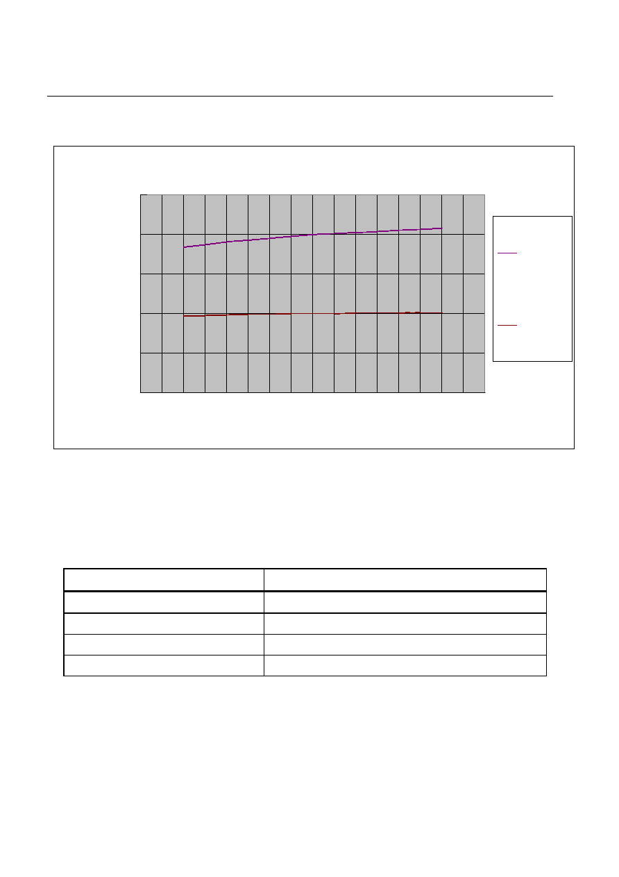
ST2016A
Ver 1.4
50/55
11/11/03
FIGURE 17-29: Relation between operation voltage & frequency
Voltage & Frequency
0.00
1.00
2.00
3.00
4.00
5.00
2.2
2.7
3.2
3.7
Voltage
MHz
RC=4MHz
RC=2MHz
TABLE 17-37: OSCI Resistance
to OSC Frequency mapping table
OSCI Resistance
OSC Frequency
185K 4MHz
442K 2MHz
965K 1MHz
2080K 0.5MHz
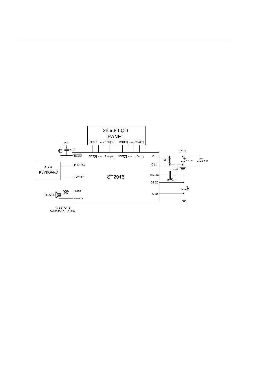
ST2016A
Ver 1.4
51/55
11/11/03
1
1
8
8
.
.
A
A
p
p
p
p
l
l
i
i
c
c
a
a
t
t
i
i
o
o
n
n
C
C
i
i
r
r
c
c
u
u
i
i
t
t
s
s
18.1 APPLICATION CIRCUIT UNDER 3V OPERATING VOLTAGE
VDD : 3V
Clock : 32768Hz crystal and 4.0MHz RC oscillator
LCD : 1/8 duty
I/O : PORT A
ALARM
: PSGO, PSGOB
FIGURE 18-30: APPLICATION CIRCUIT WITHOUT LCD KEYBOARD AWAKING PULSE
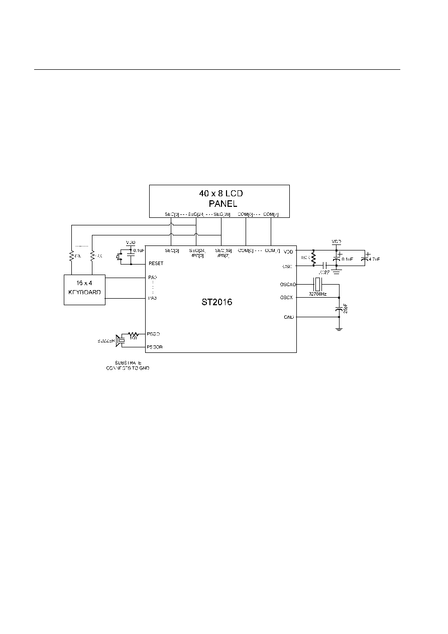
ST2016A
Ver 1.4
52/55
11/11/03
VDD : 3V
Clock : 32768Hz crystal and 4.0MHz RC oscillator
LCD : 1/8 duty
I/O
: PORT A
ALARM
: PSG0, PSG1
FIGURE 18-31: APPLICATION CIRCUIT WITH LCD KEYBOARD AWAKING PULSE
Note:
1. COMs and SEGs output GND level, while the LCD is turned off.
2. If LCD is turned off, Keyboard Awaking Pulses must be turned off at the
same time.
3. Connect one capacitor of 100PF to OSCI stabilize oscillation frequency.
This capacitor must be placed close to OSCI.

ST2016A
Ver 1.4
53/55
11/11/03
1
1
9
9
.
.
R
R
E
E
V
V
E
E
R
R
S
S
E
E
Version 1.4:
Page 8
Modifying Memory mapping diagram.
Page 47
Modifying example code and flow chart.....................................................2003/11/03
Version 1.3:
Page51/52
Modifying Reset pin connect a switch to VDD in Application Circuit.................2003/8/22
Version 1.2:
Page 42
Adding the Measure Condition on TABLE 15-33:
Page 49
Modifying the DC Charateristic
Page 51/52
Modifying the Application Circuit (1000P 100P)..........................................2003/8/4
Version 1.1:
Page 1
Modifying operation voltage range..
Page 5
Fill pad description..................................................................................2003/7/8
Version 1.0:
Page 19
Modifying the description of Port-D.
Page 43
Fill LCD Power Consumption.
Page 50
Fill electrical characteristic table .
Page 51
Add FIGURE 17-29: & TABLE 17-37: ......................................................2003/7/4
Version 0.4:
Page 48/49
Modifying FIGURE 18-30: /FIGURE 18-31: and note.
Version 04:
Page 3
Adding Pad Diagram.
Page 19
Modifying TABLE 10-17: (SCAN) to (COM).
Page 49/50
Modifying FIGURE 18-30: /FIGURE 18-31: and note
Page 51
Adding Pad Location...............................................................................2003/1/29
Version 03:
Page 27
Adding TABLE 13-25: to describe register "PSGC2"
Page 43
Modifying example for using keyboard scan function.
Page 12
Adding register "PAK" description.
Page 19
Adding exposition of port-D.
Page 41
Modifying the LCD source clock table..........................................................2002/12/9
Version 0.2:
Page 40
Modifying the driving strength table.............................................................2002/10/29
Version 0.1:
......................................................................................................................................2002/10/1