ST
ST
ST
ST
Sitronix
ST2104
PRELIMINARY
8 BIT Microcontroller with 512K bytes ROM
Notice: This is not a final specification. Some parameters are subject to change.
Ver 0.5
1
/
44 2002-Feb-18
1
1
.
.
F
F
E
E
A
A
T
T
U
U
R
R
E
E
S
S
Totally static 65C02S CPU
ROM: 512K x 8-bit
RAM: 4K x 8-bit
Stack: Up to 128-level deep
Operation voltage:
- Logic: 2.4V ~ 5.5V
- DC-DC voltage converter: 2.4V ~ 3.4V
Built-in double DC-DC voltage converter for LCD driver
I/O ports
- 24 CMOS bidirectional bit programmable I/O pins
- Bit programmable pull-up for input pins
- Hardware de-bounce option for Port-A
Low voltage detector
Timer/Counter:
- Two 8-bit timer/16-bit event counter
- One 8-bit Base timer
6 hardware interrupts with dedicated exception vectors
- External interrupt (edge triggered)
- Timer0 interrupt
- Timer1 interrupt
- Base timer interrupt
- Port-A interrupt (transition triggered)
- DAC reload interrupt
Dual clock sources with warm-up timer
- Low frequency crystal oscillator
����������������������������������������������������
32768 Hz
- RC oscillator
�������������������������������������������
500K ~ 4M Hz
- High frequency crystal/resonator oscillator (code option)
����������������������������������������������
455K~4M Hz
Direct memory access (DMA)
- Block-to-Block move
- Block to Single port
LCD controller/driver
- 16-level contrast control
- 1168 (73x16) dots (1/16 duty, metal option)
- 1560 (65x24) dots (1/24 duty, metal option)
Programmable sound generator (PSG)
- Two channels with three playing modes
- Tone/noise generator
- 16-level volume control
PWM DAC: Three modes up to 8-bit resolution
Three power down modes:
- WAI0 mode
- WAI1 mode
- STP mode
2
2
.
.
G
G
E
E
N
N
E
E
R
R
A
A
L
L
D
D
E
E
S
S
C
C
R
R
I
I
P
P
T
T
I
I
O
O
N
N
The ST2104 is a W65C02S based 8-bit microcontroller
designed with CMOS silicon gate technology. This single chip
microcontroller is useful for translator, databank and other
consumer applications. It integrates with SRAM, mask ROM,
LCD controller/driver, DC-DC voltage converter, I/O ports,
timers, PSG and PWM DAC. This chip also builds in dual
oscillators for the chip performance enhancement.
Sitronix ST2104
Ver 0.5
2/44
2002-Feb-18
3
3
.
.
P
P
A
A
D
D
D
D
I
I
A
A
G
G
R
R
A
A
M
M
104
105
106
107
108
109
110
111
112
113
114
115
116
117
118
119
120
121
122
123
124
1
2
3
4
5
6
7
8
9 10 11 12 13 14 15 16 17 18 19 20 21 22 23 24 25 26 27
91 90 89 88 87 86 85 84 83 82 81 80 79 78 77 76 75 74 73 72 71 70 69 68 67 66 65
PB3
PB6
PB7
PC2
PC3
PC4
PC5
PC6
PC7
OSCXO
OSCXI
OSCI
XIO
GND
VDD
CAP1+
V1
VP
CO
M
1
2
CO
M
1
3
CO
M
1
4
CO
M
1
5
SEG
0
(CO
M
16)
SEG
1
(CO
M
17)
SEG
2
(CO
M
18)
SEG
3
(CO
M
19)
SEG
4
(CO
M
20)
SEG
5
(CO
M
21)
SEG
6
(CO
M
22)
SEG
7
(CO
M
23)
SEG
8
(S
EG0
)
SEG
9
(S
EG1
)
SEG
10
(S
EG2
)
SEG
11
(S
EG3
)
SEG
12
(S
EG4
)
SEG
13
(S
EG5
)
SEG
14
(S
EG6
)
SEG
15
(S
EG7
)
SEG
16
(S
EG8
)
SEG
17
(S
EG9
)
SEG
18
(S
EG1
0
)
SEG
19
(S
EG1
1
)
SEG
20
(S
EG1
2
)
CO
M
0
CO
M
1
CO
M
2
CO
M
3
CO
M
4
CO
M
5
CO
M
6
CO
M
7
CO
M
8
CO
M
9
CO
M
1
0
CO
M
1
1
SEG
72
(S
EG6
4
)
SEG
71
(S
EG6
3
)
SEG
70
(S
EG6
2
)
SEG
69
(S
EG6
1
)
SEG
68
(S
EG6
0
)
SEG
67
(S
EG5
9
)
SEG
66
(S
EG5
8
)
SEG
65
(S
EG5
7
)
SEG
64
(S
EG5
6
)
SEG
63
(S
EG5
5
)
SEG
62
(S
EG5
4
)
SEG
61
(S
EG5
3
)
SEG
60
(S
EG5
2
)
SEG
59
(S
EG5
1
)
SEG
58
(S
EG5
0
)
ST2104
92
TEST
95
96
97
98
99
100
101
102
103
PA6
PB1
PB2
93
94
PA0
32
33
52
51
50
49
48
47
46
45
44
43
42
41
40
39
38
37
36
35
34
SEG25(SEG17)
SEG26(SEG18)
SEG45(SEG37)
SEG44(SEG36)
SEG43(SEG35)
SEG42(SEG34)
SEG41(SEG33)
SEG40(SEG32)
SEG39(SEG31)
SEG38(SEG30)
SEG37(SEG29)
SEG35(SEG27)
SEG34(SEG26)
SEG33(SEG25)
SEG32(SEG24)
SEG31(SEG23)
SEG30(SEG22)
SEG29(SEG21)
SEG28(SEG20)
SEG27(SEG19)
SEG36(SEG28)
62
61
60
59
58
57
56
55
54
53
SEG55(SEG47)
SEG54(SEG46)
SEG53(SEG45)
SEG52(SEG44)
SEG51(SEG43)
SEG50(SEG42)
SEG49(SEG41)
SEG48(SEG40)
SEG47(SEG39)
SEG46(SEG38)
64
63
SEG57(SEG49)
SEG56(SEG48)
28
29
31
30
SEG21(SEG13)
SEG22(SEG14)
SEG24(SEG16)
SEG23(SEG15)
125
CAP1-
126
V5
127
V4
128
V3
129
V2
PA1
PA2
PA3
PA4
PA5
PA7
PB0
PC1
PC0
PB4
PB5
RESET
Sitronix ST2104
Ver 0.5
3/44
2002-Feb-18
4
4
.
.
B
B
L
L
O
O
C
C
K
K
D
D
I
I
A
A
G
G
R
R
A
A
M
M
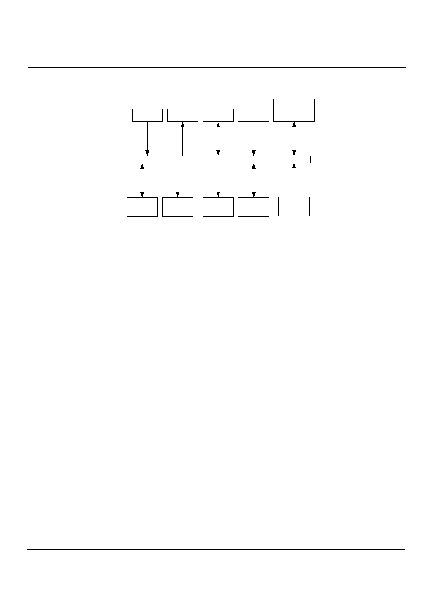
CLOCK
GENERATOR
LCD
RAM
ROM
TIMER
PSG
DAC
PORT
CPU
LOW
VOLTAGE
DETECTOR
Sitronix ST2104
Ver 0.5
4/44
2002-Feb-18
5
5
.
.
P
P
A
A
D
D
D
D
E
E
S
S
C
C
R
R
I
I
P
P
T
T
I
I
O
O
N
N
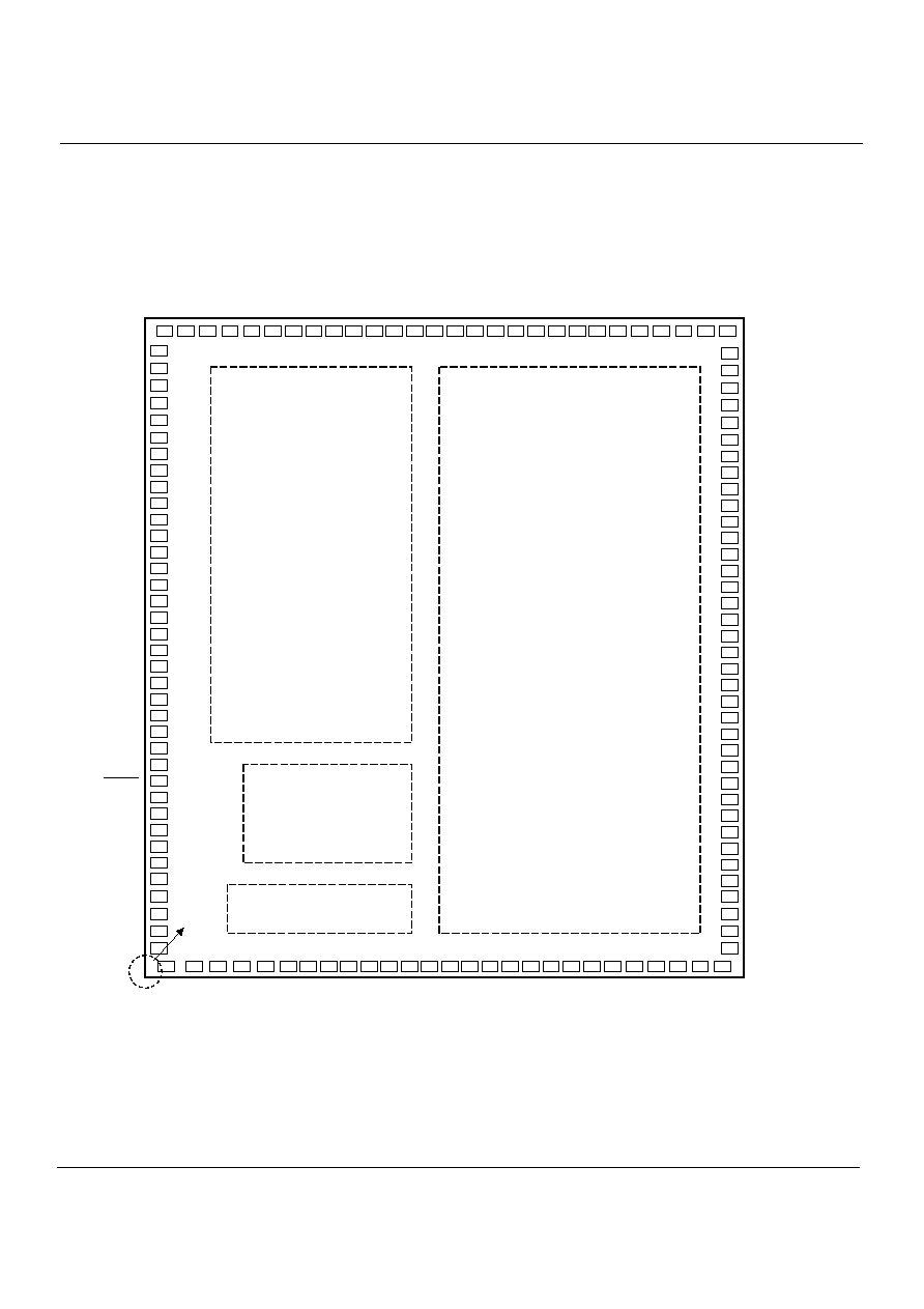
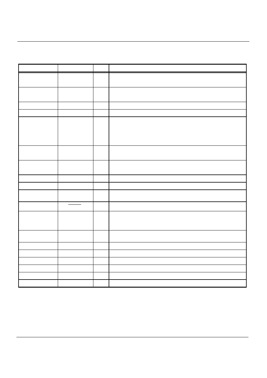
Pin No.
Designation
I/O
Description
7~14 SEG0(COM16)~
SEG7(COM23)
O
O
- LCD segment drives 0~7 (1/16 duty mode)
- LCD common drives 16~32 (1/24 duty mode)
15~79 SEG8(SEG0)~
SEG72(SEG64)
O
O
- LCD segment drives 8~72 (1/16 duty mode)
- LCD segment drives 0~64 (1/24 duty mode)
91~80, 3~6
COM0~11, 12~15
O
LCD common drives 0~15
92
TEST
I
Chip test function. Leave it open.
93 PA0
/
INTX
I/O
I
I
I
- Port-A bit programmable I/O
- Edge-trigger Interrupt.
- Transition-trigger Interrupt
- Programmable Timer1 clock source
94~100 PA1~7
I/O
I
- Port-A bit programmable I/O
- Transition-trigger Interrupt
101,102 PB0,
1
I/O
O
- Port-B bit programmable I/O
- PSG/DAC Output
103~108
PB2~7
I/O
Port-B bit programmable I/O
109~116
PC0~7
I/O
Port-C bit programmable I/O
117, 118
OSCXO, OSCXI
I/O
Low frequency crystal oscillator I/O pins. Connect to external 32768 Hz
crystal.
119
RESET
I
Reset signal input (low active)
120 OSCI
I
I
- RC oscillator input pin. Connected to external resistor
- High frequency crystal/resonator oscillator input pin. Connect to external
crystal/resonator.
121
XIO
O
High frequency crystal/resonator oscillator output pin. Connect to external
crystal/resonator.
122 GND
P
Ground
123 VCC
P
Power
supply
124
CAP1+
I/O
Connect to booster capacitor positive(+) terminal
125
CAP1-
I/O
Connect to booster capacitor negative(-) terminal
1, 129~126
V1, V2~V5
I
Inputs of external power supply for LCD drives
2
VP
O
Voltage output of booster circuit
Note: I = input, O = output, I/O = input/output, P = power.
Sitronix ST2104
Ver 0.5
5/44
2002-Feb-18
6
6
.
.
C
C
P
P
U
U
Register Model
7
0
A
7
0
Y
7
0
X
7
0
PCH PCL
7
0
1 S
Accumulator A
Index Register Y
Index Register X
Program Counter PC
Stack Pointer S
Accumulator (A)
The Accumulator is a general-purpose 8-bit register that stores
the results of most arithmetic and logic operations. In addition,
the accumulator usually contains one of the two data words
used in these operations.
Index Registers (X,Y)
There are two 8-bit Index Registers (X and Y), which may be
used to count program steps or to provide and index value to
be used in generating an effective address. When executing an
instruction, which specifies indexed addressing, the CPU
fetches the OP code and the base address, and modifies the
address by adding the index register to it prior to performing
the desired operation. Pre or post-indexing of indirect
addresses is possible.
Stack Pointer (S)
The Stack Pointer is an 8-bit register, which is used to control
the addressing of the variable-length stack. It's range from
100H to 1FFH total for 256 bytes (128 level deep). The stack
pointer is automatically increment and decrement under control
of the microprocessor to perform stack manipulations under
direction of either the program or interrupts (IRQ). The stack
allows simple implementation of nested subroutines and
multiple level interrupts. The stack pointer is initialized by the
user's software.
Program Counter (PC)
The 16-bit Program Counter register provides the address,
which step the microprocessor through sequential program
instructions. Each time the microprocessor fetches and
instruction from program memory, the lower byte of the
program counter (PCL) is placed on the low-order bits of the
address bus and the higher byte of the program counter (PCH)
is placed on the high-order 8 bits. The counter is increment
each time an instruction or data is fetched from program
memory.
Status Register (P)
The 8-bit Processor Status Register contains seven status flags.
Some of these flags are controlled by program; others may be
controlled both by the program and the CPU. The instruction
set contains a member of conditional branch instructions that
are designed to allow testing of these flags. Refer to TABLE 6-1
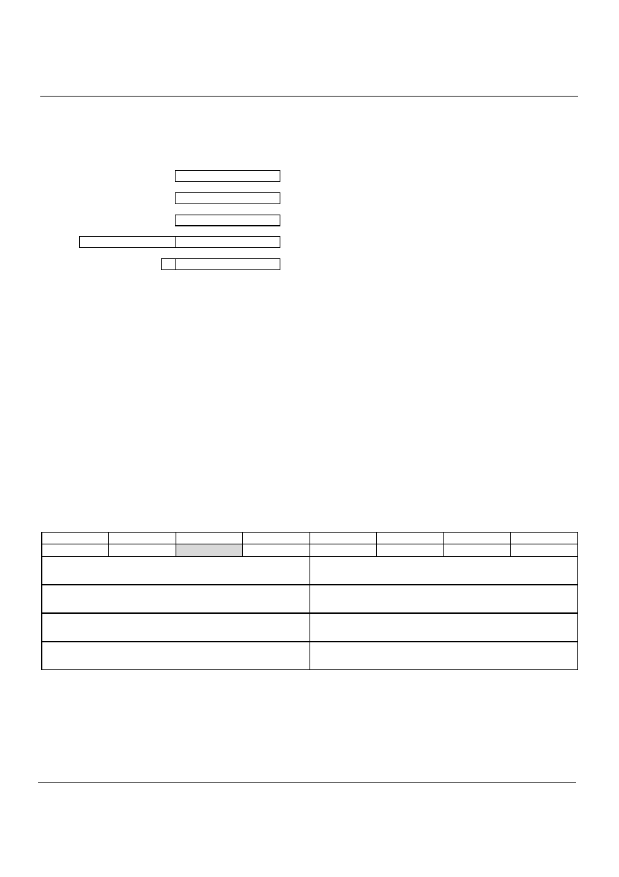
TABLE 6-1 Status Register (P)
Bit 7
Bit 6
Bit 5
Bit 4
Bit 3
Bit 2
Bit 1
Bit 0
N V 1
B D I Z C
Bit 7: N : Signed flag by arithmetic
1 = Negative
0 = Positive
Bit 3: D : Decimal mode flag
1 = Decimal mode
0 = Binary mode
Bit 6: V : Overflow of signed Arithmetic flag
1 = Negative
0 = Positive
Bit 2: I : Interrupt disable flag
1 = Interrupt disable
0 = Interrupt enable
Bit 1: Z : Zero flag
1 = Zero
0 = Non zero
Bit 4: B : BRK interrupt flag
1 = BRK interrupt occur
0 = Non BRK interrupt occur
Bit 0: C : Carry flag
1 = Carry
0 = Non carry