ST
ST2204
PRELIMINARY
8 BIT Integrated Microcontroller with 512K Bytes ROM
Notice: This is not a final specification. Some parameters are subject to change.
Ver 0.5
1
/
22 10/20/03
1
1
.
.
F
F
E
E
A
A
T
T
U
U
R
R
E
E
S
S
Totally static 8-bit CPU
ROM: 512K x 8-bit
RAM: 10K x 8-bit
Stack: Up to 128-level deep
Operation voltage: 2.4V ~ 3.6V
Operation frequency:
� 3.0Mhz@2.4V(Min.)
� 4.0Mhz@2.7V(Min.)
Low Voltage Detector (LVD)
Low Voltage Reset (LVR)
Memory interface to ROM, RAM, Flash
Memory configuration
� Three kinds of bank for program, data and interrupts
� 12-bit bank register supports up to 44M bytes
� 6 programmable chip-selects with 4 modes
� Maximum single device of 16M bytes at
CS5
General-Purpose I/O (GPIO) ports
� 48 multiplexed CMOS bidirectional bit programmable
I/Os
� Hardware de-bounce option for Port-A
� Bit programmable pull-up for input pins
� Bit programmable pull-up/down and open-drain/CMOS
for Port-C
Programmable Watchdog Timer (WDT)
Timer/Counter
� Two 8-bit timer, one can be a 16-bit event counter
� One 8-bit Base timer with 5 coexistent interrupt time
settings
Three clocking outputs
� Clock sources including Timer0/1, baud rate generator
11 prioritized interrupts with dedicated exception
vectors
� External interrupt (edge triggered)
� TIMER0 interrupt
� TIMER1 interrupt
� BASE timer interrupt
� PORTA interrupt (transition triggered)
� DAC reload interrupt
� LCD buffer interrupt
� SPI interrupt (x2)
� UART interrupts (x2)
Dual clock sources with warm-up timer
� Low frequency crystal oscillator (OSCX)
��������������������������������������������������� 32768 Hz
� RC oscillator (OSC)��������������������������������500K ~ 4M Hz
� High frequency crystal/resonator oscillator
(Bonding
option)������455K~4M
Hz
Direct Memory Access (DMA)
� Block-to-Block transfer
� Block to Single port
LCD Controller (LCDC)
� Software programmable screen size up to 320X240
� Support 1-, 4-bit LCD data bus
� Share system memory with display memory
� Large display area with small internal RAM buffer is
possible to free more internal RAM for temporary
access
� Unique internal bus for memory sharing with no loss of
the CPU time
� Diverse functions including virtual screen, panning,
scrolling, contrast control and alternating signal
generator
� Gray level support: Hardware 4 levels/Software 31 levels
Universal Asynchronous Receiver/Transmitter (UART)
� Full-duplex operation
� Baud rate generator with one digital PLL
� Standard baud rates of 600 bps to 115.2 kbps
� Direct glueless support of IrDA physical layer protocol
� Two sets of I/Os (TX,RX) for two independent devices
Serial Peripheral Interface (SPI)
� Master and slave modes
� 5 serial signals including enable and data-ready
� One stage buffer for transmitter and receiver for
continuous data exchange
� Programmable data length from 7-bit to 16-bit
Programmable Sound Generator (PSG)
� Two channels with three playing modes
� Tone/noise generator
� 16-level volume control
� 8-bit PWM DAC for speech/voice
� Two dedicated outputs for directly driving and large
current
Three power down modes
� WAI0 mode
� WAI1 mode
� STP mode
10/20/03
ST2204
Ver 0.5
2/22
10/20/03
2
2
.
.
G
G
E
E
N
N
E
E
R
R
A
A
L
L
D
D
E
E
S
S
C
C
R
R
I
I
P
P
T
T
I
I
O
O
N
N
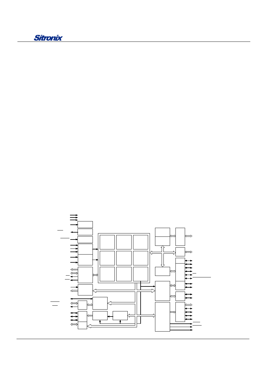
The ST2204 is a 8-bit integrated microcontroller designed with
CMOS silicon gate technology. The true static CPU core,
power down modes and dual oscillators design makes the
ST2204 suitable for power saving and long battery life designs.
The ST2204 integrates various logic to support functions
on-chip which are needed by system designers. This is also
important for lower system complexity, small board size and, of
course, shorter time to market and less cost.
The ST2204 features the capacity of memory access of
maximum 44M bytes which is needed by products with large
data bases, and also DMA function for fast memory transfer.
Six chip selects are equipped for direct connection to external
ROM, SRAM, Flash memory or other devices. Maximum one
single device of 16M bytes is possible.
The ST2204 has 48 I/Os grouped into 6 ports, Port-A ~ Port-E
and Port-L. Each pin can be programmed to input or output.
There are two options: pull-up/down for inputs of Port-C and
only pull-up for inputs of the other ports. In case of output,
there are open-drain/CMOS options for outputs of PortC and
only CMOS for the other ports. Port-A/B is designed for
keyboard scan with de-bounce and transition triggered interrupt
at Port-A, while Port-C/D/E/L are shared with other system
functions. All the properties of I/O pins are still programmable
when they are assigned to another function. This enlarges the
flexibility of the usage of function signals.
The ability of driving large LCD panels, up to 320x240, and
hardware/software gray-level support may rich the display
information and the diversity of contents as well. This is done
with no need of external display RAM because of the internal
memory sharing design. The variable LCD buffer design also
make large panel size with little internal RAM possible. User
may free major internal RAM for computing or temporary
access while keeping the display content.
The ST2204 equips serial communication ports of one UART
and one SPI to perform different communications, ex.: RS-232
and IrDA, with system components or other products such as
PC, Notebook, and popular PDA. Three clocking outputs can
produce synthesized PWM signals or high frequency carrier for
IR remote control. This helps products become more useful in
our daily life.
The built-in two channel PSG/one channel PWM DAC are for
the production of key tone, melody, voice, and speech. Two
dedicated pins with large driving capacity can drive a
buzzer/speaker directly for minimum cost.
The ST2204 has one Low Voltage Detector (LVD) for power
management. The status of internal or external power can be
detected and reported to the management software.
Power bouncing during power on is a major problem when
designing a reliable system. The ST2204 equips Low Voltage
Reset function to keep whole system in reset status when
power is low. After the power backs to normal, the system may
recover its original states and keeps working correctly.
With these integrated functions inside, the ST2204 single chip
microcontroller is a right solution for PDA, translator, databank
and other consumer products.
Clock
Generator
OSC
Clock
Generator
OSCX
OSCI
OSCXI
OSCXO
XIO
VCC/GND
TEST1/2
Power On
Reset
RESET
A[22:0]
D[7:0]
8-bit
External
Memory
Bus
RD
WR
PSG /
PWM DAC
PSGO/PSGOB
8-bit Static
CPU
ROM
512K bytes
Baud Rate
Generator
DMA
Base Timer
8-bit
SRAM
10K bytes
WDT
Interrupt
Controller
Bank
Control
Logic
PA7~0
Port-A
De-bounce
Logic
Transition
Detector
PB7~0
Port-B
UART with
IrDA Mode
SPI
INTX/PC0
Port-C
SCK/PC1
MISO/PC2
MOSI/PC3
TXD0/PC6
Port-C
RXD0/PC7
Port-C
ICE2/3
Chip Select
Logic
MMD/CS0
Port-D
Timer 0/1
8-bit
Clocking
Output
Port-E
TCO0/PE0
PE7~2
Port-E
LCD
Controller
Port-L
LD[3:0]/PL3~0
CP/PL4
AC/PL5
LOAD1/PL6
FLM/PL7
TXD1/PD6
RXD1/PD7
Port-D
/PC5
DATA_READY
/PC4
SS
0
~
/PD4
1
~
CS5
/PD5
/A23
CS6
POFF
BLANK
TCO1/PE1
BCO/PE2
PVCC/PGND
XMD
LOAD2
Low Voltage
Detector
VIN
Low Voltage
Reset
/ICE1
LVR
FIGURE 2-1 ST2204 Block Diagram
10/20/03
ST2204
Ver 0.5
3/22
10/20/03
3
3
.
.
S
S
I
I
G
G
N
N
A
A
L
L
D
D
E
E
S
S
C
C
R
R
I
I
P
P
T
T
I
I
O
O
N
N
S
S
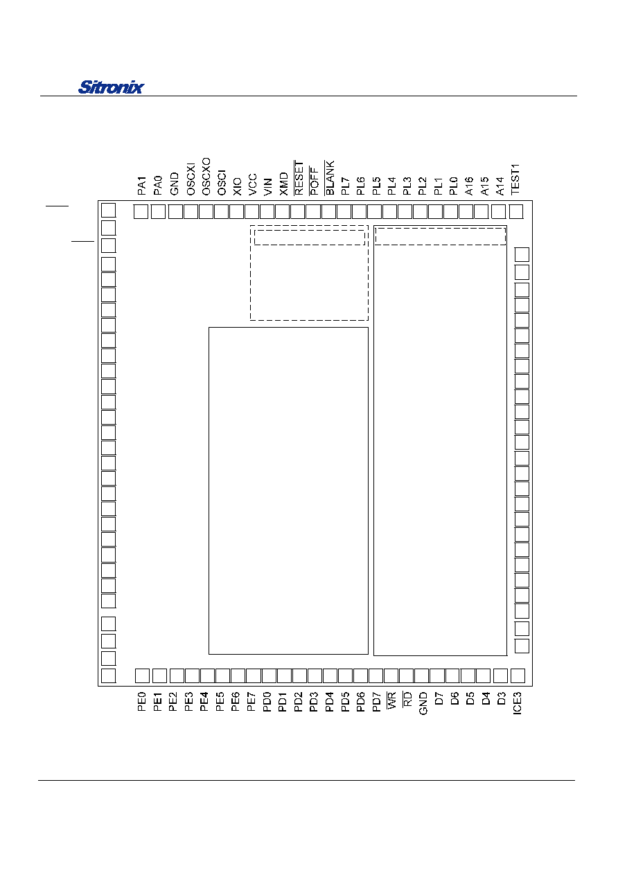
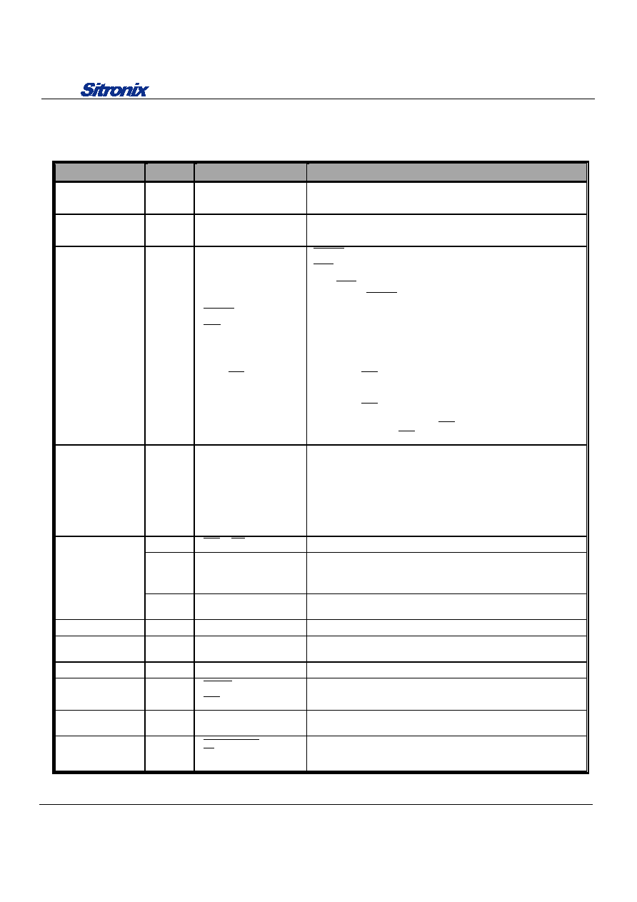
TABLE 3-1 Signal Function Groups
Function Group
Pad No.
Designation
Description
Power
18, 55,
94
VCC , PVCC
VCC:
Power supply for system
PVCC:
Power supply for PSGO and PSGOB
Ground
23, 51,
52, 74
GND , PGND
GND:
System power ground
PGND:
Power ground for PSGO and PSGOB
System control
15,
26
50,80
1,81
28
RESET ,
LVR
/ICE1,
ICE2/3,
TEST1/2,
MMD/
CS0
RESET :
Active low system reset signal input
LVR /
ICE1:
LVR : Low voltage reset signal output, connect this pin to
RESET
to make Low Voltage Reset function work.
ICE1
: ICE1 function when in ICE mode
TEST1/2, ICE2/3:
Leave them open when normal operation
MMD/CS0:
Memory modes selection pin
Normal mode:
Enable internal ROM.
MMD/
CS0
connects to GND.
Emulation mode:
Disable internal ROM.
MMD/
CS0
connects to chip-select pin of external ROM.
One resistor should be added between VCC and this pin.
After reset cycles, MMD/
CS0
changes to be an output, and
outputs signal
CS0
.
Clock
16,
19~22
XMD,
XIO,OSCI
OSCXO,OSCXI, ,
XMD:
High frequency oscillator (OSC) mode selection input
Low:
Crystal mode. One crystal or resonator should be
connected between OSCI and XIO
High:
Resistor oscillator mode. One resistor should be
connected between OSCI and VCC
OSCXI, OSCXO:
Connect one 32768Hz crystal between these
two pins when using low frequency oscillator
72, 73
WR , RD
External memory R/W control signals
2~4,
85~93,
95~105
A[22:0]
External memory address bus
External memory
bus signals
75~79,
82~84
D[7:0]
External memory data bus
PSG/PWM DAC
53, 54
PSGO, PSGOB
PSG outputs. Connect to one buzzer or speaker
Keyboard scan
signal (return line)
24~25,
27,29~33 PA7~0
I/O port A
GPIO 34~41
PB7~0
I/O
port
B
Chip selects
64~69
1
~
CS5
/PD4~0,
CS6
/A23/PD5
I/O port D and chip-select outputs
UART
48, 49,
70, 71
RXD0/PC7,TXD0/PC6,
RXD1/PD7,TXD1/PD6
UART signals and I/Os
SPI 43~47
DATA_READY
/PC5 ,
SS
/PC4 , MOSI/PC3 ,
MISO/PC2 , SCK/PC1
SPI signals and I/Os