
ST
Sitronix
ST7065C
40CH Segment/Common Driver for Dot Matrix LCD
V1.4a
2001/08/29
1/13
!"
Functions:
#"
Dot matrix LCD driver with two 20 channel
outputs
#"
Selectable function to use common/segment
drivers simultaneously
#"
Bias voltage (V1 ~ V6)
#"
Input/output signals
!"
Input : Serial display data and control
pulse from controller IC
!"
Output : 20 X 2 channels waveform for
LCD driving
!"
Features:
#"
Display driving bias : static to 1/5
#"
Power supply for logic : 2.7V ~ 5.5V
#"
Power supply for LCD voltage (V
DD
~V
EE
) :
3V ~ 11V
#"
64 Pin QFP package and bare chip available
!"
Description:
ST7065C is a segment/common driver for dot
matrix type LCD display. It features 40 channels
with 20 X 2 bits bi-directional shift registers, data
latches, LCD drivers and logic control circuits. It
is fabricated by high voltage CMOS process with
low current consumption.
The ST7065C can convert serial data received
from a LCD controller, such as ST7066U, into
parallel data and send out LCD driving
waveforms to the LCD panel. The ST7065C is
designed for general-purpose LCD drivers. It can
drive both static and dynamic drive LCD. The LSI
can be used as segment/common driver.
The ST7065C has pin function compatibility with
the KS0065B that allows the user easily to
replace it with a ST7065C.

ST7065C
V1.4a
2001/08/29
2/13
ST7065C Specification Revision History
Version Date
Description
1.1 2000/07/31
First
Edition
1.2
2000/11/14 Added QFP Pad Configuration(Page 4)
1.3 2001/04/18
Moved QFP Package Dimensions(Page 13) to Page 4
Change Shift Register Table(Page 8)
1.4
2001/05/04 ST7065 Transition to ST7065C
1.4a
2001/08/29 Added "Substrate connect to VDD"(Page 3)
ST7065C
V1.4a
2001/08/29
3/13
1
2
3
4
5
6
7
8
9
10
11
12
13
14
15
16
17
18
19
Size : 2310x1830m
Coordinate : center
Min. PAD Pitch : 120m
PAD Size : 85x90m
(0,0)
G798E
"G798E" Marking : Easy to find the PAD
59
58
57
56
55
54
53
52
51
50
49
32
33
34
35
36
37
38
39
40
41
42
43
44
45
46
47
48
31
20
21
22
23
24
25
26
27
28
29
30
Substrate connect to VDD.
!"
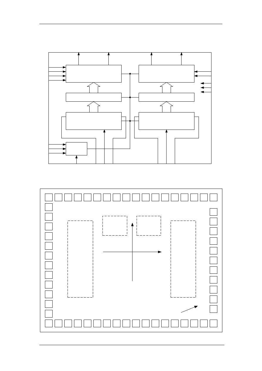
Functional Block Diagram
!"
Pad Arrangement
SEGMENT DRIVER
SEGMENT DRIVER
BIDIRECTIONAL
SHIFTER(20bits)
BIDIRECTIONAL
SHIFTER(20bits)
DATA LATCH(20bits)
DATA LATCH(20bits)
CONTOL
V1
V2
V3
V4
CL2
CL1
M
DL1 SHL1 DR1
DL2 SHL2 DR2
V
DD
V
SS
V
EE
S1...............................S20
S21...............................S40
V5
V6
FCS
ST7065C
V1.4a
2001/08/29
4/13
!"
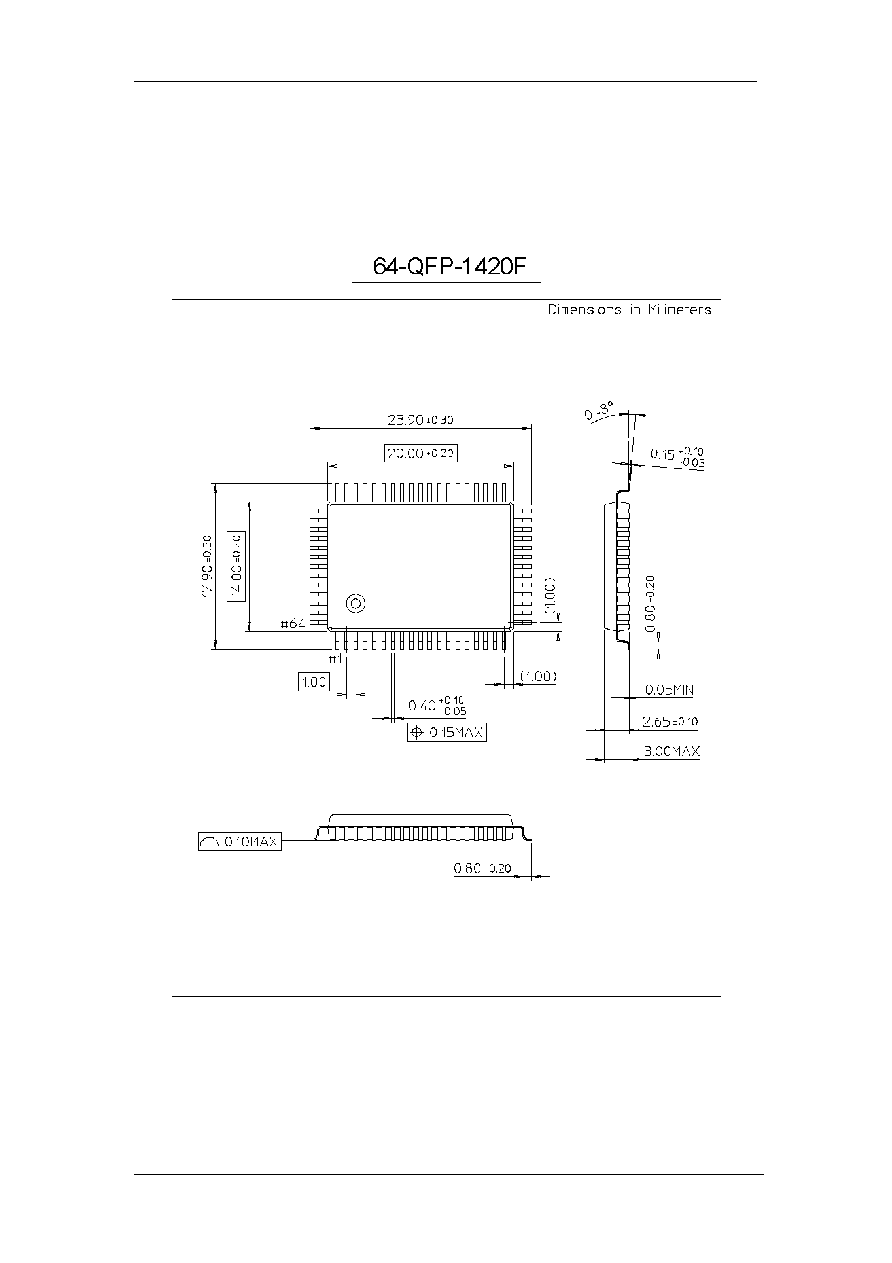
Package Dimensions
ST7065C
V1.4a
2001/08/29
5/13
!"
Pad Configuration(QFP 64)
N
C
S
3
4
S
3
3
S
3
2
S
3
1
S
3
0
N
C
S
3
5
S
3
6
S
3
7
S
3
8
S
3
9
S
4
0
S
0
9
S
1
0
S
1
1
S
0
8
S
0
7
V
D
D
N
C
S
0
6
S
0
5
S
0
4
S
0
3
S
0
2
S
0
1
6
4
6
3
6
2
6
1
6
0
5
9
5
8
5
7
5
6
5
5
5
4
5
3
5
2
2
0
2
1
2
2
2
3
2
4
2
5
2
6
2
7
2
8
2
9
3
0
3
1
3
2
NC
S29
S28
S27
S26
S25
S24
S23
S22
S21
S20
S19
S18
S17
S16
S15
S14
S13
S12
V6
V5
V4
V3
V2
V1
FCS
SHL2
SHL1
M
NC
DR2
DL2
DR1
DL1
VSS
CL2
CL1
VEE
1
2
3
4
5
6
7
8
9
10
11
12
13
14
15
16
17
18
19
51
50
49
48
47
46
45
44
43
42
41
40
39
38
37
36
35
34
33

ST7065C
V1.4a
2001/08/29
6/13
!"
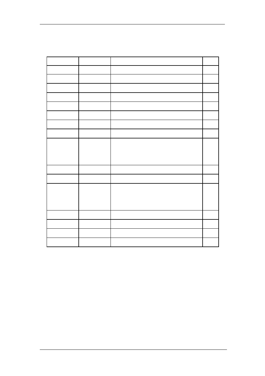
Pad Name and Coordinates
Pad No. Pad Name
X
Y
Pad No. Pad Name
X
Y
1 VEE
-1045
-670
31 S[28]
1040
800
2 CL1
-1040
-805
32 S[27]
910
805
3 CL2
-910
-805
33 S[26]
780
805
4 VSS
-780
-805
34 S[25]
660
805
5 DL1
-660
-805
35 S[24]
540
805
6 DR1 -540 -805
36 S[23] 420 805
7 DL2
-420
-805
37 S[22]
300
805
8 DR2 -300 -805
38 S[21] 180 805
9 M
-180
-805
39
S[20]
60
805
10 SHL1 -60 -805
40 S[19] -60 805
11 SHL2 60 -805
41 S[18] -180 805
12 FCS 180 -805
42 S[17] -300 805
13 V1 300 -805
43 S[16] -420 805
14 V2 420 -805
44 S[15] -540 805
15 V3 540 -805
45 S[14] -660 805
16 V4 660 -805
46 S[13] -780 805
17 V5 780 -805
47 S[12] -910 805
18 V6 910
-805
48 S[9]
-1040
800
19 S[40] 1040 -800 49 S[10] -1045 670
20 S[39] 1045 -623 50 S[11] -1045 540
21 S[38] 1045 -488 51 S[8] -1045 420
22 S[37] 1045 -358 52 S[7] -1045 300
23 S[36] 1045 -233 53 VDD -1045 180
24 S[35]
1045
-108
54 S[6] -1045 60
25 S[30]
1045 20
55 S[5] -1045
-60
26 S[31]
1045 145
56 S[4] -1045
-180
27 S[32]
1045 270
57 S[3] -1045
-300
28 S[33]
1045 395
58 S[2] -1045
-420
29 S[34]
1045 525
59 S[1] -1045
-540
30 S[29]
1045 655
ST7065C
V1.4a
2001/08/29
7/13
!"
Pin Description:
Pin Name
Purpose
Description
I/O
VDD POWER
for
logic
N/A
VSS GROUND
for
logic
N/A
VEE
LCD GND
for LCD driving voltage
N/A
V1 V2
LCD output
used as select voltage level
I
V3 V4
LCD output
Used as non select voltage level for Part I
I
V5 V6
LCD output
Used as non select voltage level for Part II
I
S[1]-S[20]
segment
LCD driver output for part 1
O
SHL1
direction
direction control for part 1 segments
I
DL1, DR1
data in /out
If SHL1 = 1 then DL1=out, DR1=in
If SHL1 = 0 then DL1=in, DR1=out
I/O
S[21]-S[40]
segment
LCD driver output for part 2
O
SHL2
direction
direction control for part 2 segments
I
DL2, DR2
data in/out
If SHL2 = 1 then DL2=out, DR2=in
If SHL2 = 0 then DL2=in, DR2=out
I/O
M
alternation
Alternate the LCD driving waveform
I
CL1
latch clock
latch the data after shift is completed
I
CL2
shift clock
shift the data into the segments
I
FCS
mode selection
mode select signal for Part II
I

ST7065C
V1.4a
2001/08/29
8/13
!"
Functional Description:
Shift Registers and Data I/O
The
ST7065C
supplies two sets of shift register, which controls the shift direction by
SHL1 & SHL2. The DL1, DR1, DL2 and DR2 are data input or output option
function.
Shift Direction of Channel 1
SHL1 Shift
Direction DL1 DR1
0 S[1]
$ S[20]
IN
OUT
1 S[20]
$ S[1]
OUT
IN
Clock and Mode Selection
In channel 1 part, the CL1 is the clock to latch data on the falling edge. It latches the
data input from the bi-directional shift register at the falling edge of CL1 and transfers
its outputs to the LCD driver circuit. The CL2 is the clock to shift data on the falling
edge. It shifts the serial data at the falling of CL2 and transfers the output of each bit
of the register to the latch circuit.
In channel 2 part, the CL1 and CL2 is the clock to latch or shift data on the falling or
rising edge which is depend on FCS value. When FCS is low, the channel 2 function
is the same as channel 1 as a segment driver. When FCS is high, the channel 2
function will become a common driver. Detail functions are show in the following
table:
FCS
Clock Eage
Channel 1
Channel 2
Latch data
Latch Data
CL1
---- ----
Shift data
Shift data
0
CL2
---- ----
Latch
data ----
CL1
----
Shift
data
Shift
data ----
1
CL2
----
Latch
data
Shift Direction of Channel 2
SHL2 Shift
Direction DL2 DR2
0 S[21]
$ S[40]
IN
OUT
1 S[40]
$ S[21]
OUT
IN
ST7065C
V1.4a
2001/08/29
9/13
!"
LCD Output Waveform
The output levels of channel1 and channel2 are decided by the combination of FCS,
M, and latched data. Refer to the following table:
FCS
Latched Data
M
Channel 1
Channel 2
1 V1 V2
1
0 V2 V1
1 V3 V6
1
0
0 V4 V5
1 V1 V1
1
0 V2 V2
1 V3 V5
0
0
0 V4 V6
Note:
To use the same function of channel 1 and channel 2 as a segment driver, V3 and V5, V4 and V6
need to short respectively.
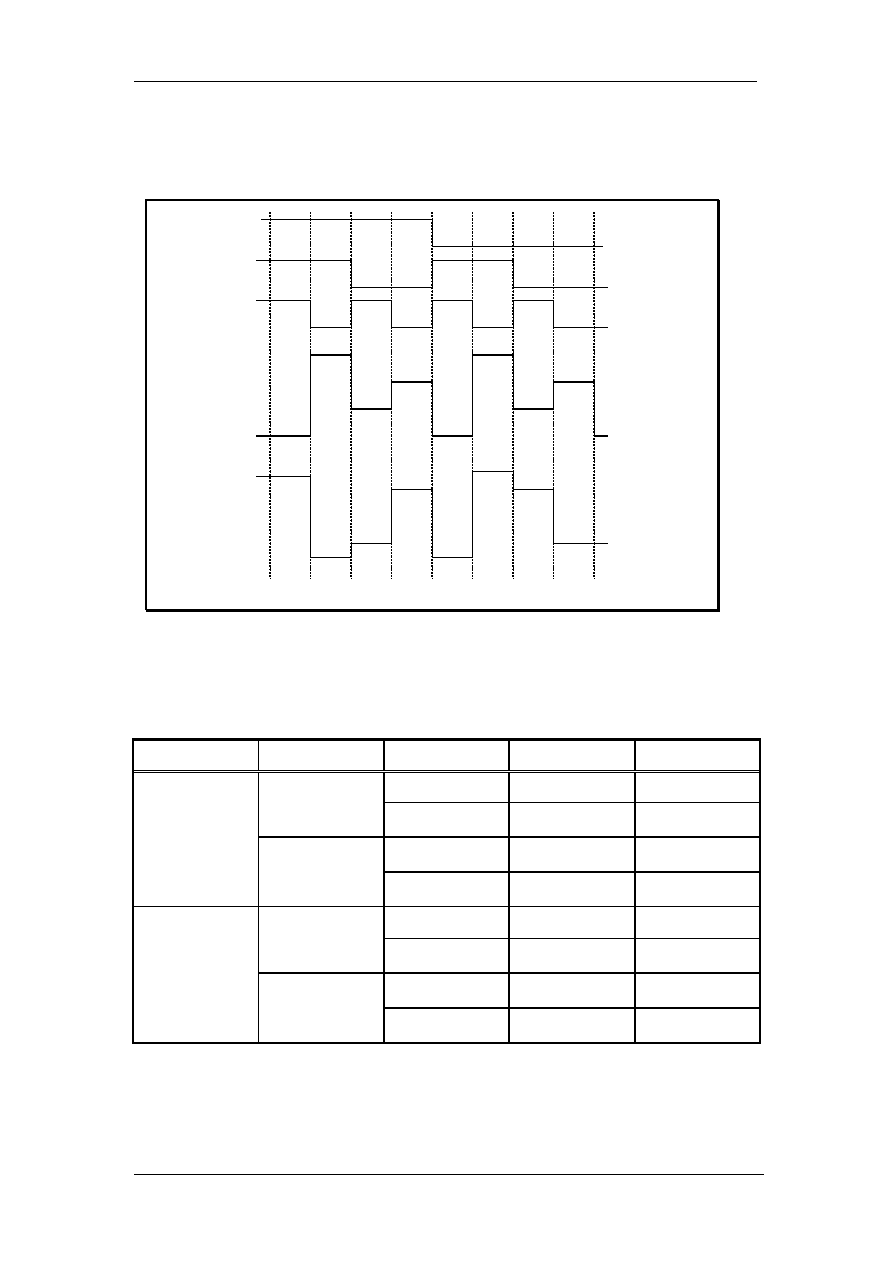
Output of LATCH
DATA
M
Channel1 Output
(S[1] ~ S[20])
V1 V1
V2
V3
V4
V2
V3
V4
FCS
V2
V1
V6
V5
V1
V2
V5
V6
Channel2 Output
(S[21] ~ S[40])

ST7065C
V1.4a
2001/08/29
10/13
Channel 1 used as a segment driver and channel 2 as a common driver (FCS=1)
When channel 2 is used as a common driver, FCS is connected to VDD. Channel 2
will shift data on the rising edge of CL1 and latch data on the rising edge of CL2.
Both Channels 1 and 2 used as segment drivers (FCS=0)
When both channels 1 and 2 of the
ST7065C
are used as segment drivers, they will
shift data on the falling edge of CL2 and latch data on the falling edge of CL1.
V3&V5, V4&V6 are shorted in the application circuit as shown in the following
figure.
LCD
Controller
D
CL1
CL2
M
DL1
CL1
CL2
M
V1
V2
V3
V4
V1 V2 V3 V4 V5 V6
S[1] � S[40]
ST7065C
FCS
SHL1
SHL2
VSS
To LCD Segment
DR1
DL2
DR2
V6
LCD
Controller
D
CL1
CL2
M
FLM
DL1
CL1
CL2
M
DL2
V1
V2
V3
V4
V5
V1 V2 V3 V4 V5 V6
S[1] � S[20]
S[21] � S[40]
ST7065C
FCS
SHL1
SHL2
VDD
VSS
To LCD Segment
To LCD Common
ST7065C
V1.4a
2001/08/29
11/13
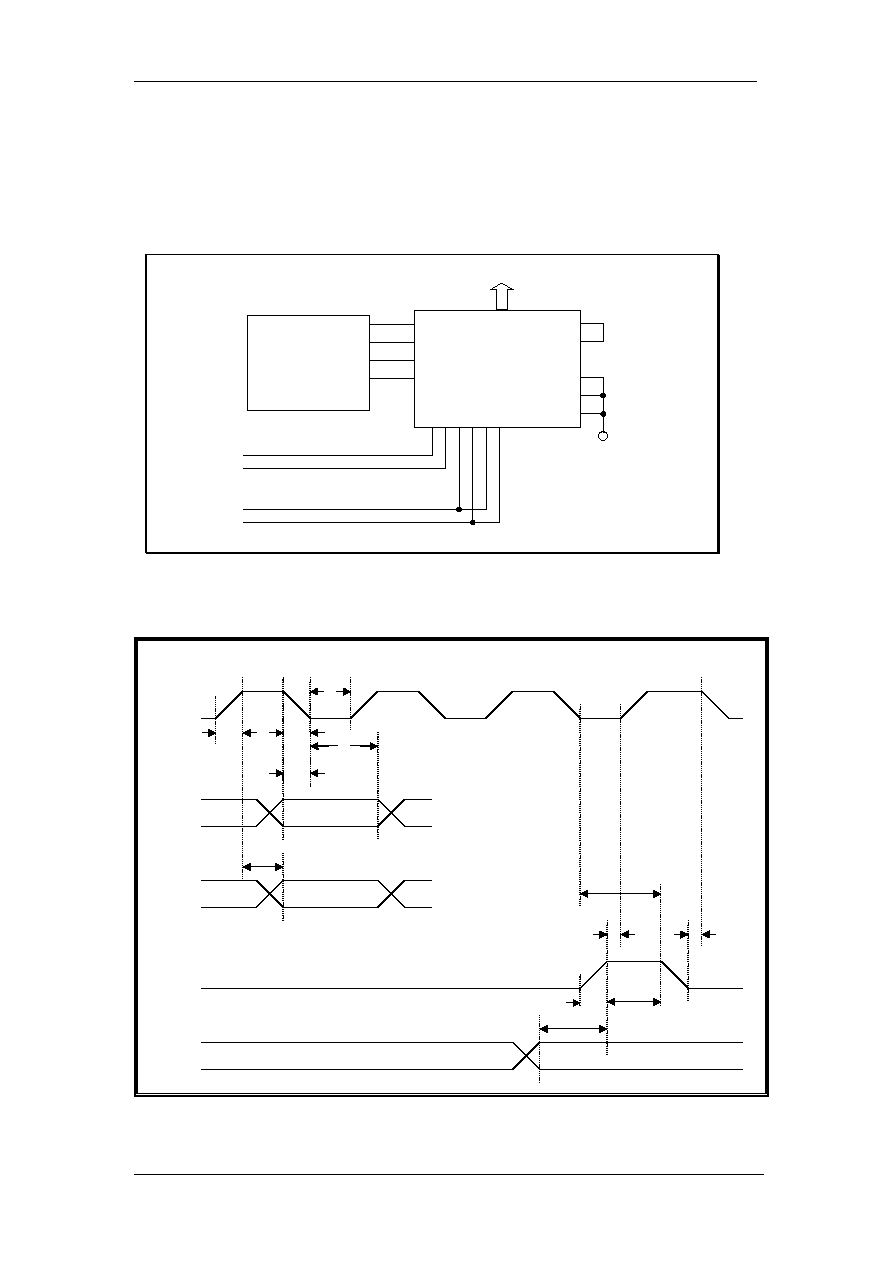
Both Channels 1 and 2 used as common drivers (FCS=0)
When both channels 1 and 2 of the
ST7065C
are used as common drivers, the FCS is
set low and the signals (CL1, CL2, M) from the controller are connected as shown in
the following figure.
!"
Timing Characteristics
CL2
Data in
(DL1, DL2)
(DR1, DR2)
Data out
(DL1, DL2)
(DR1, DR2)
CL1
M
V
IH
V
IL
T
R
T
WCKH
T
F
T
WCKL
T
DH
T
SU
T
D
V
OH
V
OL
T
SL
T
LS
T
LS
T
WCKH
T
R
T
SU
V6
LCD
Controller
FLM
CL1
CL2
M
DL1
CL1
CL2
M
V1
V2
V5
V1 V2 V3 V4 V5 V6
S[1] � S[40]
ST7065C
FCS
SHL1
SHL2
VSS
To LCD Common
DR1
DL2
DR2
ST7065C
V1.4a
2001/08/29
12/13
!"
D.C Characteristics:
Symbol
Parameter
Test Condition Min. Typ. Max. Unit Applicable pin
VDD Operating
Voltage
-
2.7 - 5.5
V
-
VLCD
Driver Supply Voltage
VDD-VEE
3
-
11
V
-
VIH
Input High Voltage
-
0.7
VDD
- VDD
V
VIL
Input Low Voltage
-
0
-
0.3
VDD
V
ILKG
Input Leakage Current
VIN = 0 ~ VDD
-5
-
5
uA
CL1,CL2,M,SHL1,S
HL2
DL1,DL2,DR1,DR2
VOH
Output High Voltage
IOH = -0.4mA
VDD
-0.4
- -
V
VOL
Output Low Voltage
IOL = +0.4mA
-
-
0.4
V
DL1,DL2,DR1,DR2
V1~V6, S[1]~S[40]
IDD
Operating Current
FCL2 = 400KHZ
-
100
300
uA
VDD,VEE
IV
Leakage Current
VIN = VDD ~ VEE
-10
-
10
uA
V1 ~ V6
!"
A.C Characteristics:
Symbol Parameter
Test
Condition
Min. Max. Unit Applicable pin
FCL
Data Shift Frequency
-
-
400
KHZ
CL2
TWCKH
Clock High Level Width
-
800
-
ns
CL1,CL2
TWCKL
Clock Low Level Width
-
800
-
ns
CL2
TSL
Clock Set-up Time
CL2 $ CL1
500
-
ns
CL1,CL2
TLS
Clock Set-up Time
CL1 $ CL2
500
-
ns
CL1,CL2
TR/TF
Clock Rise/Fall Time
-
-
200
ns
CL1,CL2
TSU
Data Set-up Time
-
300
-
ns
DL1,DL2,DR1,DR2
TDH
Data Hold Time
-
300
-
ns
DL1,DL2,DR1,DR2
TD
Data Delay Time
CL = 15 PF
-
500
ns
DL1,DL2,DR1,DR2
!"
Maximum Absolute Ratings:
Symbol Parameters Min.
Max.
Unit
VDD Supply
Voltage -0.3
7
V
TOPR Operating
Temperature -20 75
TSTG Storage
Temperature -55 125
ST7065C
V1.4a
2001/08/29
13/13
!"
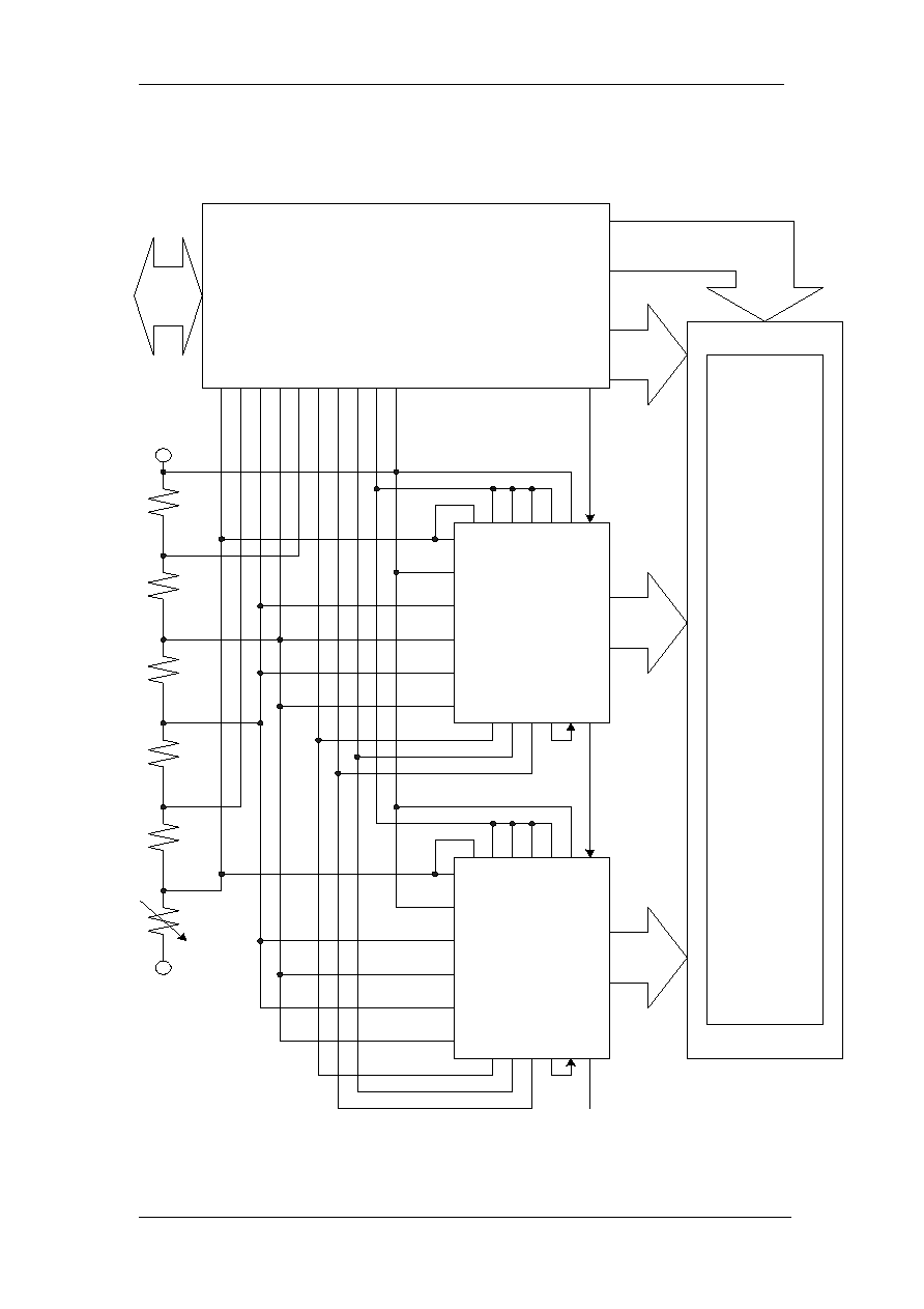
Application Circuit: (2Line x 24Word)
ST7066U
ST7065C
ST7065C
Dot Matrix LCD Panel
-V or GND
Vcc(+5V)
Regsister
Regsister
Regsister
Regsister
Regsister
VR
DB0-DB7
To MPU
V5
V4
V3
V2
V1
M
CL1
CL2
GND
VCC
Seg 1-40
Com 1-16
VEE
VSS
SHL2
SHL1
FCS
VDD
DL1
V1
V2
V3
V4
V5
V6
V1
V2
V3
V4
V5
V6
VEE
VSS
SHL2
SHL1
FCS
VDD
DL1
M
CL2
CL1
DR1
DL2
DR2
M
CL2
CL1
DR1
DL2
DR2
Seg 1-40
Seg 1-40
Note:
Regsister=2.2K~10K ohm
VR=10K~30Kohm
D