ChipFind - документация

Электронный компонент: ST7567

Скачать:  PDF   ZIP
ST
Sitronix
ST7565
65 x 132 Dot Matrix LCD Controller/Driver
Ver 1.0a
1/56
2002/06/24
F
F
E
E
A
A
T
T
U
U
R
R
E
E
S
S
Direct display of RAM data through the display data
RAM.
RAM capacity : 65 x 132 = 8580 bits
Application Display driver circuits
1/65 duty : 65 common x 132 segment
1/49 duty : 49 common x 132 segment
1/33 duty : 33 common x 132 segment
1/55 duty : 55 common x 132 segment
1/53 duty : 53 common x 132 segment
High-speed 8-bit MPU interface (The chip can be
connected directly to the both the 80x86 series MPUs
and the 68000 series MPUs)
/Serial interfaces are supported.
Abundant command functions
Display data Read/Write, display ON/OFF, Normal/
Reverse display mode, page address set, display start
line set, column address set, status read, display all
points ON/OFF, LCD bias set, electronic volume,
read/modify/write, segment driver direction select,
power saver, static indicator, common output status
select, V
5
voltage regulation internal resistor ratio set.
Static drive circuit equipped internally for indicators.
(1 system, with variable flashing speed.)
Low-power liquid crystal display power supply circuit
equipped internally.
Booster circuit (with Boost ratios of Double/Triple/
Quad, where the step-up voltage reference power
supply can be input externally).
High-accuracy voltage adjustment circuit (Thermal
gradient 0.15%/C or external input) V
5
voltage
regulator resistors equipped internally, V
1
to V
4
voltage
divider resistors equipped internally, electronic volume
function equipped internally, voltage follower.
CR oscillator circuit equipped internally (external
clock can also be input)
Extremely low power consumption Operating power
when the built-in power supply is used (an example)
95uA (V
DD
V
SS
= V
DD
V
SS2
=5.0 V, Quad voltage,
V
5
V
DD
= 11.0 V).
Conditions: When displays pattern OFF and the
normal mode is selected.
Power supply Operable on the low 2.0 voltage
Logic power supply V
DD
V
SS
= 4.0V to 5.5 V
Boost reference voltage: V
DD
V
SS2
= 2.0V to 5.5V
Booster maximum voltage limited V
OUT
= -18V
Liquid crystal drive power supply:
V
DD
V
5
= 4.0V to 13.0 V
Wide range of operating temperatures: 40 to 85C
CMOS process
Shipping forms include bare chip and TCP.
Not support master/slave mode
These chips not designed for resistance to light or
resistance to radiation.
G
G
E
E
N
N
E
E
R
R
A
A
L
L
D
D
E
E
S
S
C
C
R
R
I
I
P
P
T
T
I
I
O
O
N
N
The ST7565 is a single-chip dot matrix LCD drivers that can
be connected directly to a microprocessor bus. 8-bit parallel
or serial display data sent from the microprocessor is stored
in the internal display data RAM and the chip generates a
LCD drive signal independent of the microprocessor.
Because the chips in the ST7565 contain 65x132 bits of
display data RAM and there is a 1-to-1 correspondence
between the LCD panel pixels and the internal RAM bits,
these chips enable displays with a high degree of freedom.
The ST7565chips contain 65 common output circuits and 132
segment output circuits, so that a single chip can drive a
65x132 dot display (capable of displaying 8 columnsx4 rows
of a 16x16 dot kanji font).
Moreover, the capacity of the display can be extended
through the use of master/slave structures between chips.
The chips are able to minimize power consumption
because no external operating clock is necessary for the
display data RAM read/write operation. Furthermore,
because each chip is equipped internally with a low-power
LCD driver power supply, resistors for LCD driver power
voltage adjustment and a display clock CR oscillator circuit,
the ST7565 can be used to create the lowest power display
system with the fewest components for high-performance
portable devices.
PART NO.
V
RS
temperature gradient
V
RS
range
ST7565-0A -0.15%/C -2.1V 0.06V
ST7565-0B External
input
---
ST7565
Ver 1.0a
2/56
2002/06/24
P
P
I
I
N
N
D
D
I
I
M
M
E
E
N
N
S
S
I
I
O
O
N
N
S
S
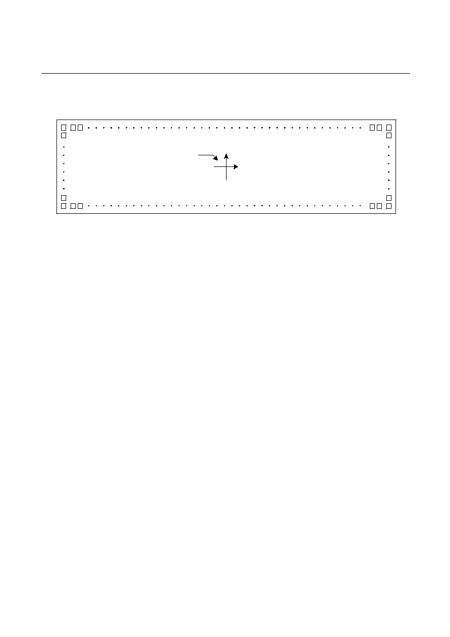
Chip Size
9760 m X 2440 m
Bump Pitch
65 m (Min.)
Bump Size
PAD No. 1~24
85 m X 85 m
PAD No. 25~82
64 m X 85 m
PAD No. 83~99
85 m X 85 m
PAD No. 100
85 m X 73 m
PAD No. 101~133
85 m X 47 m
PAD No. 134
85 m X 73 m
PAD No. 135
73 m X 85 m
PAD No. 136~273
47 m X 85 m
PAD No. 274
73 m X 85 m
PAD No. 275
85 m X 73 m
PAD No. 276~308
85 m X 47 m
PAD No. 309
85 m X 73 m
Bump Height
18 m (Typ.)
Chip Thickness
457 m

Master/slave mode cancel.
VOUT maximum -18V
ST7565-0A Temperature gradient = -0.15%/C
Logic power supply V
DD
V
SS
= 4.0V to 5.5 V
Booster 4 times cancel , 3 times , 2 times worked
In display reverse mode , used display off command : display pixels all on
In display reverse mode , used display all point on command : display pixels all off
(0,0)
ST7565
Die No.
1
309
275
274
135
134
100
99
ST7565
Ver 1.0a
3/56
2002/06/24
P
P
a
a
d
d
C
C
e
e
n
n
t
t
e
e
r
r
C
C
o
o
o
o
r
r
d
d
i
i
n
n
a
a
t
t
e
e
s
s
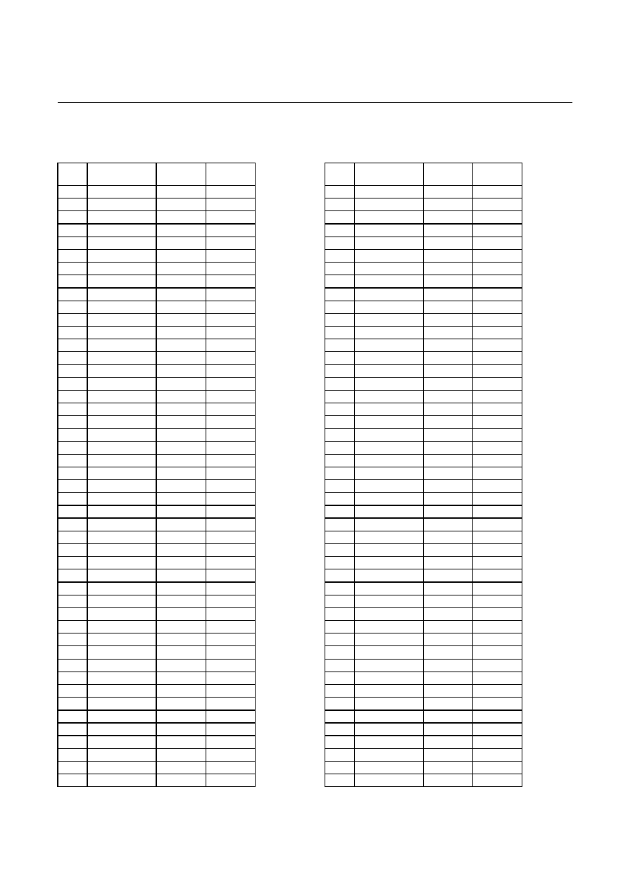
Units: m
PAD
No.
PIN Name
X
Y
001
(NC)
4536
1117
002
FRS
4431
1117
003
FR
4326
1117
004
CL
4221
1117
005
/DOF
4116
1117
006
(NC)
4011
1117
007
VSS
3906
1117
008
/CS1
3801
1117
009
CS2
3696
1117
010
VDD
3591
1117
011
/RES
3486
1117
012
A0
3381
1117
013
VSS
3276
1117
014
WR(R/W)
3171
1117
015
RD(E)
3066
1117
016
VDD
2961
1117
017
D0
2856
1117
018
D1
2751
1117
019
D2
2646
1117
020
D3
2541
1117
021
D4
2436
1117
022
D5
2331
1117
023
D6(SCL)
2226
1117
024
D7(SI)
2121
1117
025
(NC)
2026.5
1117
026
VDD
1942.5
1117
027
VDD
1858.5
1117
028
VDD
1774.5
1117
029
VDD
1690.5
1117
030
VSS
1606.5
1117
031
VSS
1522.5
1117
032
VSS
1438.5
1117
033
VSS2
1354.5
1117
034
VSS2
1270.5
1117
035
VSS2
1186.5
1117
036
VSS2
1102.5
1117
037
(NC)
1018.5
1117
038
VOUT
934.5
1117
039
VOUT
850.5
1117
040
CAP3-
766.5
1117
041
CAP3-
682.5
1117
042
(NC)
598.5
1117
043
CAP1+
514.5
1117
044
CAP1+
430.5
1117
045
CAP1-
346.5
1117
046
CAP1-
262.5
1117
047
CAP2-
178.5
1117
PAD
No.
PIN Name
X
Y
048
CAP2-
94.5
1117
049
CAP2+
10.5
1117
050
CAP2+
-73.5
1117
051
VSS
-157.5
1117
052
VSS
-241.5
1117
053
VRS
-325.5
1117
054
VRS
-409.5
1117
055
VDD
-493.5
1117
056
VDD
-577.5
1117
057
V1
-661.5
1117
058
V1
-745.5
1117
059
V2
-829.5
1117
060
V2
-913.5
1117
061
(NC)
-997.5
1117
062
V3
-1081.5
1117
063
V3
-1165.5
1117
064
V4
-1249.5
1117
065
V4
-1333.5
1117
066
V5
-1417.5
1117
067
V5
-1501.5
1117
068
(NC)
-1585.5
1117
069
VR
-1669.5
1117
070
VR
-1753.5
1117
071
VDD
-1837.5
1117
072
VDD
-1921.5
1117
073
TEST1
-2005.5
1117
074
TEST2
-2089.5
1117
075
TEST3
-2173.5
1117
076
TEST4
-2257.5
1117
077
TEST5
-2341.5
1117
078
TEST6
-2425.5
1117
079
TEST7
-2509.5
1117
080
TEST8
-2593.5
1117
081
TEST9
-2677.5
1117
082
TEST10
-2761.5
1117
083
VDD
-2856
1117
084
M/S
-2961
1117
085
CLS
-3066
1117
086
VSS
-3171
1117
087
C86
-3276
1117
088
P/S
-3381
1117
089
VDD
-3486
1117
090
/HPM
-3591
1117
091
VSS
-3696
1117
092
IRS
-3801
1117
093
VDD
-3906
1117
094
SEL1
-4011
1117
ST7565
Ver 1.0a
4/56
2002/06/24
PAD
No.
PIN Name
X
Y
095
VSS
-4116
1117
096
SEL2
-4221
1117
097
VDD
-4326
1117
098
SEL3
-4431
1117
099
VSS
-4536
1117
100
(NC)
-4777.5
1119
101
COM[31]
-4777.5
1040
102
COM[30]
-4777.5
975
103
COM[29]
-4777.5
910
104
COM[28]
-4777.5
845
105
COM[27]
-4777.5
780
106
COM[26]
-4777.5
715
107
COM[25]
-4777.5
650
108
COM[24]
-4777.5
585
109
COM[23]
-4777.5
520
110
COM[22]
-4777.5
455
111
COM[21]
-4777.5
390
112
COM[20]
-4777.5
325
113
COM[19]
-4777.5
260
114
COM[18]
-4777.5
195
115
COM[17]
-4777.5
130
116
COM[16]
-4777.5
65
117
COM[15]
-4777.5
0
118
COM[14]
-4777.5
-65
119
COM[13]
-4777.5
-130
120
COM[12]
-4777.5
-195
121
COM[11]
-4777.5
-260
122
COM[10]
-4777.5
-325
123
COM[9]
-4777.5
-390
124
COM[8]
-4777.5
-455
125
COM[7]
-4777.5
-520
126
COM[6]
-4777.5
-585
127
COM[5]
-4777.5
-650
128
COM[4]
-4777.5
-715
129
COM[3]
-4777.5
-780
130
COM[2]
-4777.5
-845
131
COM[1]
-4777.5
-910
132
COM[0]
-4777.5
-975
133
COMS
-4777.5
-1040
134
(NC)
-4777.5
-1119
135
(NC)
-4531.5
-1117
136
(NC)
-4452.5
-1117
137
(NC)
-4387.5
-1117
138
(NC)
-4322.5
-1117
139
SEG[0]
-4257.5
-1117
140
SEG[1]
-4192.5
-1117
141
SEG[2]
-4127.5
-1117
142
SEG[3]
-4062.5
-1117
143
SEG[4]
-3997.5
-1117
144
SEG[5]
-3932.5
-1117
145
SEG[6]
-3867.5
-1117
146
SEG[7]
-3802.5
-1117
PAD
No.
PIN Name
X
Y
147
SEG[8]
-3737.5
-1117
148
SEG[9]
-3672.5
-1117
149
SEG[10]
-3607.5
-1117
150
SEG[11]
-3542.5
-1117
151
SEG[12]
-3477.5
-1117
152
SEG[13]
-3412.5
-1117
153
SEG[14]
-3347.5
-1117
154
SEG[15]
-3282.5
-1117
155
SEG[16]
-3217.5
-1117
156
SEG[17]
-3152.5
-1117
157
SEG[18]
-3087.5
-1117
158
SEG[19]
-3022.5
-1117
159
SEG[20]
-2957.5
-1117
160
SEG[21]
-2892.5
-1117
161
SEG[22]
-2827.5
-1117
162
SEG[23]
-2762.5
-1117
163
SEG[24]
-2697.5
-1117
164
SEG[25]
-2632.5
-1117
165
SEG[26]
-2567.5
-1117
166
SEG[27]
-2502.5
-1117
167
SEG[28]
-2437.5
-1117
168
SEG[29]
-2372.5
-1117
169
SEG[30]
-2307.5
-1117
170
SEG[31]
-2242.5
-1117
171
SEG[32]
-2177.5
-1117
172
SEG[33]
-2112.5
-1117
173
SEG[34]
-2047.5
-1117
174
SEG[35]
-1982.5
-1117
175
SEG[36]
-1917.5
-1117
176
SEG[37]
-1852.5
-1117
177
SEG[38]
-1787.5
-1117
178
SEG[39]
-1722.5
-1117
179
SEG[40]
-1657.5
-1117
180
SEG[41]
-1592.5
-1117
181
SEG[42]
-1527.5
-1117
182
SEG[43]
-1462.5
-1117
183
SEG[44]
-1397.5
-1117
184
SEG[45]
-1332.5
-1117
185
SEG[46]
-1267.5
-1117
186
SEG[47]
-1202.5
-1117
187
SEG[48]
-1137.5
-1117
188
SEG[49]
-1072.5
-1117
189
SEG[50]
-1007.5
-1117
190
SEG[51]
-942.5
-1117
191
SEG[52]
-877.5
-1117
192
SEG[53]
-812.5
-1117
193
SEG[54]
-747.5
-1117
194
SEG[55]
-682.5
-1117
195
SEG[56]
-617.5
-1117
196
SEG[57]
-552.5
-1117
197
SEG[58]
-487.5
-1117
198
SEG[59]
-422.5
-1117
ST7565
Ver 1.0a
5/56
2002/06/24
PAD
No.
PIN Name
X
Y
199
SEG[60]
-357.5
-1117
200
SEG[61]
-292.5
-1117
201
SEG[62]
-227.5
-1117
202
SEG[63]
-162.5
-1117
203
SEG[64]
-97.5
-1117
204
SEG[65]
-32.5
-1117
205
SEG[66]
32.5
-1117
206
SEG[67]
97.5
-1117
207
SEG[68]
162.5
-1117
208
SEG[69]
227.5
-1117
209
SEG[70]
292.5
-1117
210
SEG[71]
357.5
-1117
211
SEG[72]
422.5
-1117
212
SEG[73]
487.5
-1117
213
SEG[74]
552.5
-1117
214
SEG[75]
617.5
-1117
215
SEG[76]
682.5
-1117
216
SEG[77]
747.5
-1117
217
SEG[78]
812.5
-1117
218
SEG[79]
877.5
-1117
219
SEG[80]
942.5
-1117
220
SEG[81]
1007.5
-1117
221
SEG[82]
1072.5
-1117
222
SEG[83]
1137.5
-1117
223
SEG[84]
1202.5
-1117
224
SEG[85]
1267.5
-1117
225
SEG[86]
1332.5
-1117
226
SEG[87]
1397.5
-1117
227
SEG[88]
1462.5
-1117
228
SEG[89]
1527.5
-1117
229
SEG[90]
1592.5
-1117
230
SEG[91]
1657.5
-1117
231
SEG[92]
1722.5
-1117
232
SEG[93]
1787.5
-1117
233
SEG[94]
1852.5
-1117
234
SEG[95]
1917.5
-1117
235
SEG[96]
1982.5
-1117
236
SEG[97]
2047.5
-1117
237
SEG[98]
2112.5
-1117
238
SEG[99]
2177.5
-1117
239
SEG[100]
2242.5
-1117
240
SEG[101]
2307.5
-1117
241
SEG[102]
2372.5
-1117
242
SEG[103]
2437.5
-1117
243
SEG[104]
2502.5
-1117
244
SEG[105]
2567.5
-1117
245
SEG[106]
2632.5
-1117
246
SEG[107]
2697.5
-1117
247
SEG[108]
2762.5
-1117
248
SEG[109]
2827.5
-1117
249
SEG[110]
2892.5
-1117
250
SEG[111]
2957.5
-1117
PAD
No.
PIN Name
X
Y
251
SEG[112]
3022.5
-1117
252
SEG[113]
3087.5
-1117
253
SEG[114]
3152.5
-1117
254
SEG[115]
3217.5
-1117
255
SEG[116]
3282.5
-1117
256
SEG[117]
3347.5
-1117
257
SEG[118]
3412.5
-1117
258
SEG[119]
3477.5
-1117
259
SEG[120]
3542.5
-1117
260
SEG[121]
3607.5
-1117
261
SEG[122]
3672.5
-1117
262
SEG[123]
3737.5
-1117
263
SEG[124]
3802.5
-1117
264
SEG[125]
3867.5
-1117
265
SEG[126]
3932.5
-1117
266
SEG[127]
3997.5
-1117
267
SEG[128]
4062.5
-1117
268
SEG[129]
4127.5
-1117
269
SEG[130]
4192.5
-1117
270
SEG[131]
4257.5
-1117
271
(NC)
4322.5
-1117
272
(NC)
4387.5
-1117
273
(NC)
4452.5
-1117
274
(NC)
4531.5
-1117
275
(NC)
4777.5
-1119
276
COM[32]
4777.5
-1040
277
COM[33]
4777.5
-975
278
COM[34]
4777.5
-910
279
COM[35]
4777.5
-845
280
COM[36]
4777.5
-780
281
COM[37]
4777.5
-715
282
COM[38]
4777.5
-650
283
COM[39]
4777.5
-585
284
COM[40]
4777.5
-520
285
COM[41]
4777.5
-455
286
COM[42]
4777.5
-390
287
COM[43]
4777.5
-325
288
COM[44]
4777.5
-260
289
COM[45]
4777.5
-195
290
COM[46]
4777.5
-130
291
COM[47]
4777.5
-65
292
COM[48]
4777.5
0
293
COM[49]
4777.5
65
294
COM[50]
4777.5
130
295
COM[51]
4777.5
195
296
COM[52]
4777.5
260
297
COM[53]
4777.5
325
298
COM[54]
4777.5
390
299
COM[55]
4777.5
455
300
COM[56]
4777.5
520
301
COM[57]
4777.5
585
302
COM[58]
4777.5
650