 | –≠–ª–µ–∫—Ç—Ä–æ–Ω–Ω—ã–π –∫–æ–º–ø–æ–Ω–µ–Ω—Ç: ST8016 | –°–∫–∞—á–∞—Ç—å:  PDF PDF  ZIP ZIP |
ST
Sitronix
ST8016
PRELIMINARY
160 Output LCD Common/Segment driver IC
Notice: This is not a final specification. Some parameters are subject to change
V1.0 1/26
2003-07-02
1. DESCRIPTION
The ST8016 is a 160-output segment/common driver
IC suitable for driving large/medium scale dot matrix
LCD panels, and is used in personal computers/work
stations. Through the use of SST (Super Slim TCP)
technology, it is ideal for substantially decreasing the
size of the frame section of the LCD module. The
ST8016 is good both as a segment driver and a
common driver, and it can create a low power
consuming, high-resolution LCD.
2. FEATURES
Number of LCD drive outputs: 160
Supply voltage for LCD drive: +15.0 to +40.0 V
Supply voltage for the logic system: +2.5 to +5.5 V
Low power consumption
Low output impedance
Package: 186-pin TCP (Tape Carrier Package)
(Segment mode)
Shift clock frequency
- 20 MHz (MAX.): V
DD
= +5.0 ± 0.5 V
- 15 MHz (MAX.): V
DD
= +3.0 to + 4.5 V
- 12 MHz (MAX.): V
DD
= +2.5 to + 3.0 V
Adopts a data bus system
4-bit/8-bit parallel input modes are selectable with a
mode (MD) pin
Automatic transfer function of an enable signal
Automatic counting function which, in the chip
selection mode, causes the internal clock to be
stopped by automatically counting 160 bits of input
data
Line latch circuits are reset when DISPOFF active
(Common mode)
Shift clock frequency: 4 MHz (MAX.)
Built-in 160-bit bi-directional shift register (divisible
into 80 bits x 2)
Available in a single mode (160-bit shift register) or in
a dual mode (80-bit shift register x 2)
Y
1
->Y
160
Single mode
Y
160
->Y
1
Single mode
Y
1
->Y
80
, Y
81
->Y
160
Dual mode
Y
160
->Y
81
, Y
80
->Y
1
Dual mode
The above 4 shift directions are pin-selectable
Shift register circuits are reset when DISPOFF active
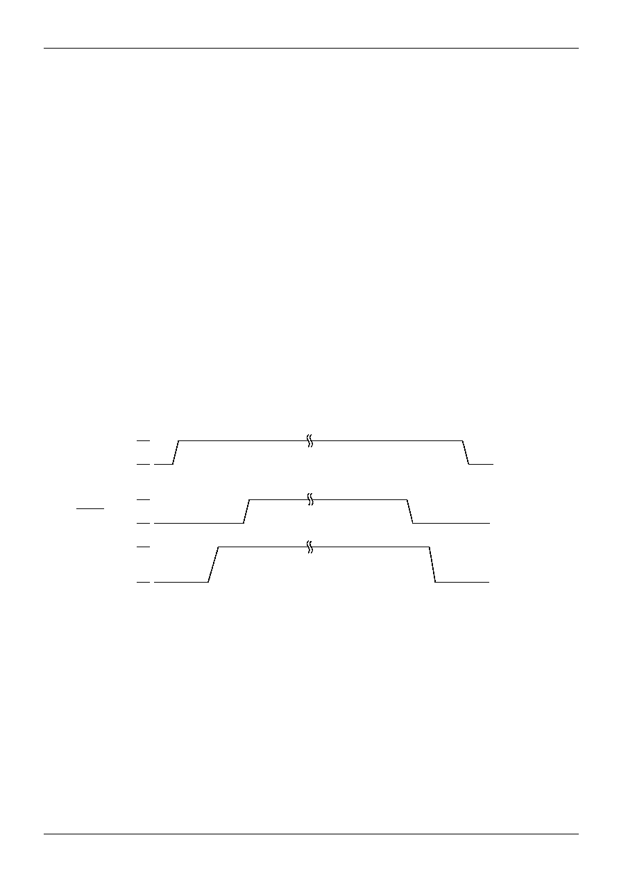
3. PIN CONNECTIONS
1
160
161
186
Y
1
Y
158
Y
159
Y
160
Y
3
Y
2
V
0R
V
0L
EIO
1
LP
DISPOFF
XCK
DI
0
EIO
2
S/C
V
DD
V
43L
V
12L
DI
1
DI
7
DI
6
DI
5
DI
4
DI
3
DI
2
FR
V
SS
V
43R
V
12R
L/R
MD
186 PIN TCP
CHIP SURF
ACE
V
SS
Sitronix ST8016
V1.0 2/26
2003-07-02
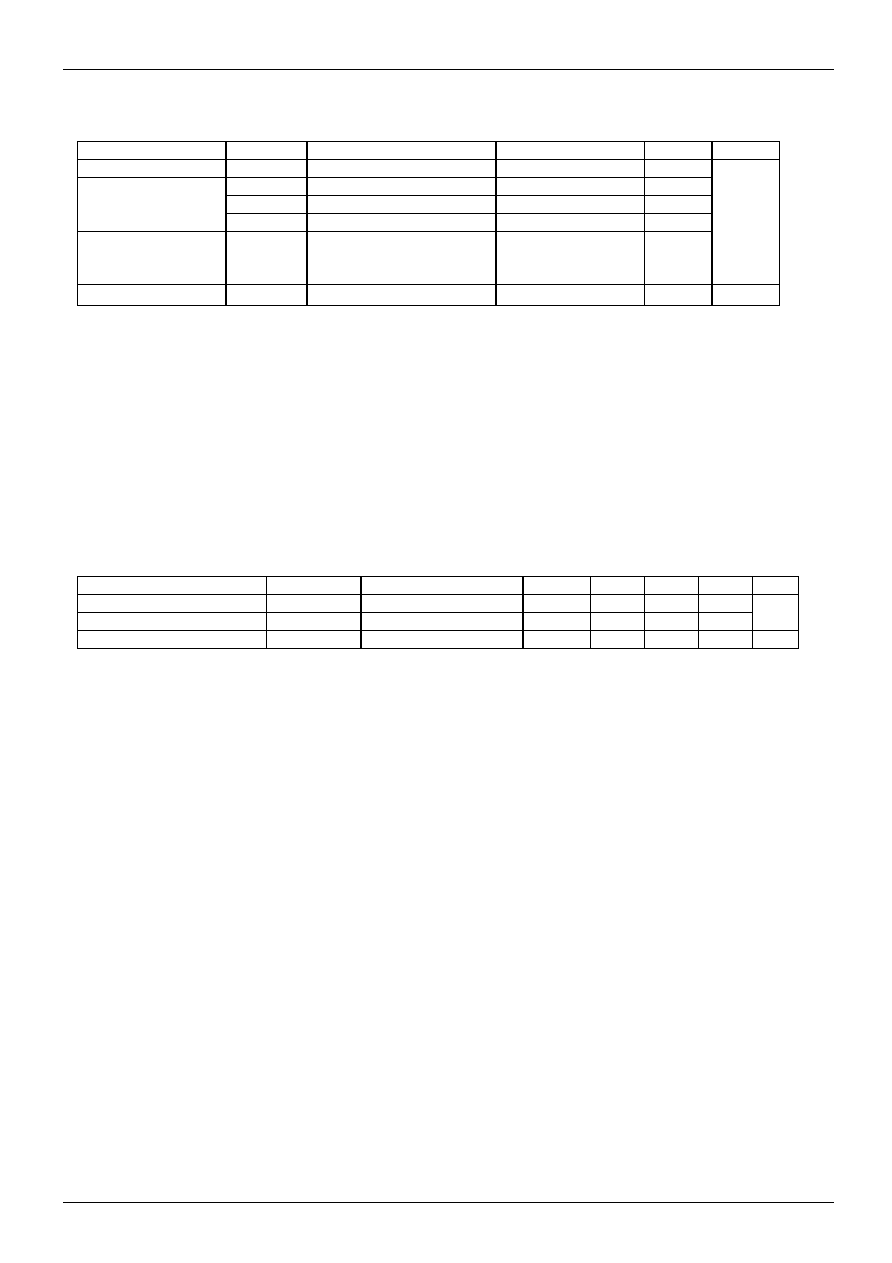
4. PIN DESCRIPTION (TCP TYPE)
PIN NO.
SYMBOL
I/O
DESCRIPTION
1 ~ 160
Y
1
-Y
160
O LCD drive output
161,186 V
0L
, V
0R
P Power supply for LCD drive
162,185 V
12L
, V
12R
P Power supply for LCD drive
163,184 V
43L
, V
43R
P Power supply for LCD drive
165
L/R
I Display data shift direction selection
166 V
DD
P Power supply for logic system (+2.5 to +5.5 V)
167
S/C
I Segment mode/common mode selection
168,180 EIO
2
, EIO
1
I/O
Input/output for chip selection at segment mode
Shift data input/output for shift register at common mode
169 ~ 175
DI
0
-DI
6
I Display data input at segment mode
176 DI
7
I Display data input at segment mode/Dual mode data input at common mode
177
XCK
I Clock input for taking display data at segment mode
178
/DISPOFF
I Control input for output of non-select level
179 LP
I Latch pulse input for display data at segment mode/
Shift clock input for shift register at common mode
181
FR
I AC-converting signal input for LCD drive waveform
182
MD
I Mode selection input
164,183 V
SS
P
Ground
(0
V)
P: power pin
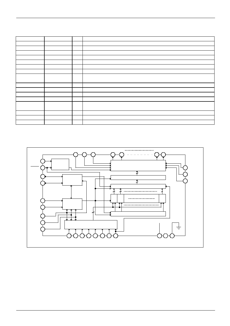
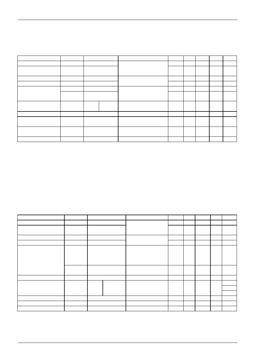
5. BLOCK DIAGRAM
160-BIT 4-LEVEL DRIVER
160-BIT LEVEL SHIFTER
160-BIT LINE LATCH/SHIFT REGISTER
DATA LATCH CONTROL
SP CONVERSION & DATA CONTROL
(4 to 8 or 8 to 8)
CONTROL
LOGIC
ACTIVE
CONTROL
LEVEL
SHIFTER
8 BIT
DATA
LATCH
DI0
DI1
DI2
DI3
DI4
DI5
DI6
DI7
V
DD
V
SS
V
43L
V
12L
V
0L
Y
160
Y
159
Y
2
Y
1
V
43R
V
12R
V
0R
FR
DISPOFF
EIO
1
EIO
2
LP
XCK
L/R
MD
S/C
8
16
16
16
160
160
Sitronix ST8016
V1.0 3/26
2003-07-02
6. FUNCTIONAL OPERATIONS OF EACH BLOCK
BLOCK FUNCTION
Active Control
In case of segment mode, controls the selection or non-selection of the chip.
Following an LP signal input, and after the chip selection signal is input, a selection signal is
generated internally until 160 bits of data have been read in.
Once data input has been completed, a selection signal for cascade connection is output, and
the chip is non-selected.
In case of common mode, controls the input/output data of bi-directional pins.
SP Conversion
& Data Control
In case of segment mode, keeps input data which are 2 clocks of XCK at 4-bit parallel input
mode in latch circuit, or keeps input data which are 1 clock of XCK at 8-bit parallel input mode
in latch circuit; after that they are put on the internal data bus 8 bits at a time.
Data Latch Control
In case of segment mode, selects the state of the data latch which reads in the data bus
signals. The shift direction is controlled by the control logic. For every 16 bits of data read in,
the selection signal shifts one bit based on the state of the control circuit.
Data Latch
In case of segment mode, latches the data on the data bus. The latch state of each LCD
drive output pin is controlled by the control logic and the data latch control; 160 bits of data are
read in 20 sets of 8 bits.
Line Latch/
Shift Register
In case of segment mode, all 160 bits which have been read into the data latch are
simultaneously latched at the falling edge of the LP signal, and are output to the level shifter
block. In case of common mode, shifts data from the data input pin at the falling edge of the LP
signal.
Level Shifter
The logic voltage signal is level-shifted to the LCD drive voltage level, and is output to the
driver block.
4-Level Driver
Drives the LCD drive output pins from the line latch/shift register data, and selects one of 4
levels (V
0
, V
12
, V
43
or V
SS
) based on the S/C, FR and /DISPOFF signals.
Control Logic
Controls the operation of each block. In case of segment mode, when an LP signal has been
input, all blocks are reset and the control logic waits for the selection signal output from the
active control block. Once the selection signal has been output, operation of the data latch and
data transmission is controlled, 160 bits of data are read in, and the chip is non-selected. In
case of common mode, controls the direction of data shift.
Sitronix ST8016
V1.0 4/26
2003-07-02
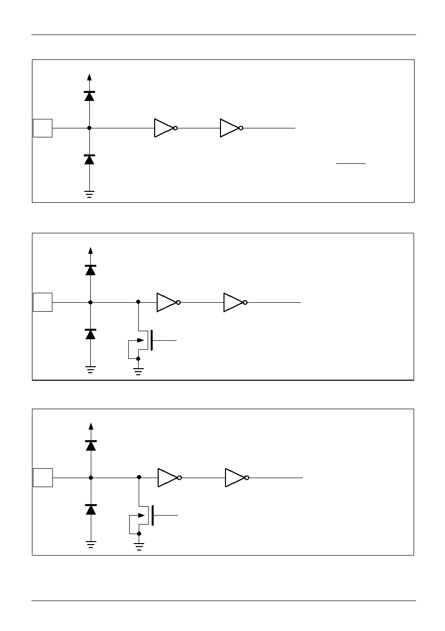
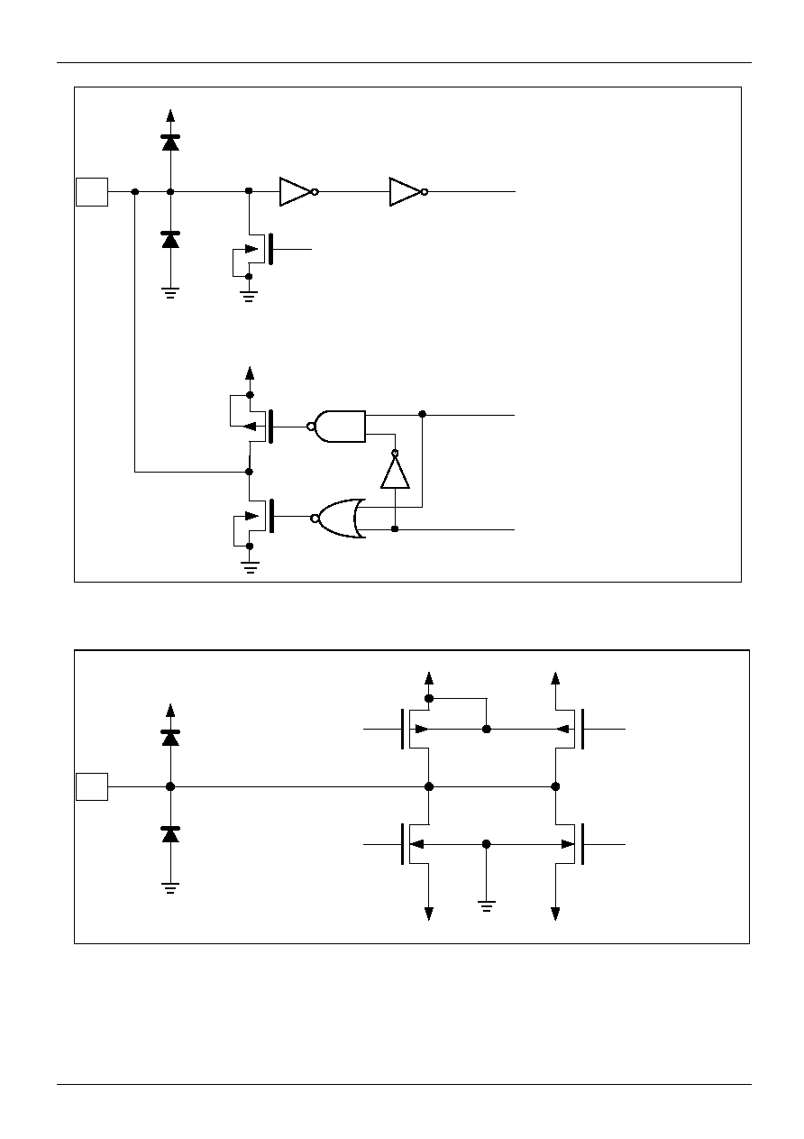
INPUT/OUTPUT CIRCUITS
I
V
DD
To Internal Circuit
Vss (0V)
Applicable Pins
L/R , S/C , DI
6
~DI
0
,
DISPOFF , LP , FR , MD
Fig. 1 Input Circuit (1)
I
V
DD
To Internal Circuit
Applicable Pins
DI
7
, XCK
Vss (0V)
Vss (0V)
Control Signal
Fig. 2 Input Circuit (2)
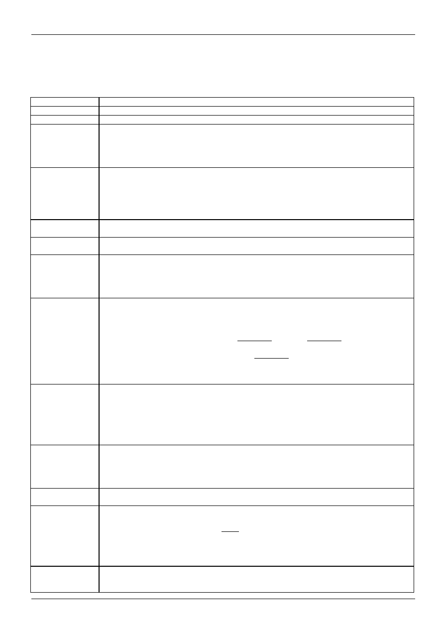
I
V
DD
To Internal Circuit
Applicable Pins
TEST
1
, TEST
2
Vss (0V)
Vss (0V)
V
DD
Fig. 3 Input Circuit (3)
Sitronix ST8016
V1.0 5/26
2003-07-02
V
DD
I/O
To Internal
Circuit
Vss (0V)
Vss (0V)
Control Signal
Vss (0V)
V
DD
Output Signal
Control Signal
Application Pins
EIO
1
, EIO
2
Fig. 4 Input/Output Circuit
O
Vss (0V)
V
0
Control Signal 1
Control Signal 3
Control Signal 2
Control Signal 4
V
0
V
12
V
43
V
5
V
SS
(0V)
Application Pins
Y
1
~Y
160
Fig. 5 LCD Drive Output Circuit
Sitronix ST8016
V1.0 6/26
2003-07-02
7. FUNCTIONAL DESCRIPTION
7.1 Pin Functions
(Segment mode)
SYMBOL FUNCTION
V
DD
Logic system power supply pin, connected to +2.5 to +5.5 V.
V
SS
Ground pin, connected to 0 V.
V
0L
, V
0R
V
12L
, V
12R
V
43L
, V
43R
Bias power supply pins for LCD drive voltage
Normally use the bias voltages set by a resistor divider
Ensure that voltages are set such that V
SS
< V
43
< V
12
< V
0
.
V
iL
and V
iR
(i = 0,12, 43) must connect to an external power supply, and supply regular
voltage which is assigned by specification for each power pin
DI
7
-DI
0
Input pins for display data
In 4-bit parallel input mode, input data into the 4 pins, DI
3
-DI
0
.
Connect DI
7
-DI
4
to V
SS
or V
DD
.
In 8-bit parallel input mode, input data into the 8 pins, DI
7
-Dl
0
.
Refer to "RELATIONSHIP BETWEEN THE DISPLAY DATA AND LCD DRIVE OUTPUT
PINS" in Functional Operations.
XCK
Clock input pin for taking display data
* Data is read at the falling edge of the clock pulse.
LP
Latch pulse input pin for display data
Data is latched at the falling edge of the clock pulse.
L/R
Input pin for selecting the reading direction of display data
When set to V
SS
level "L", data is read sequentially from Y
160
to Y
1
.
When set to V
DD
level "H", data is read sequentially from Y
1
to Y
160
.
Refer to "RELATIONSHIP BETWEEN THE DISPLAY DATA AND LCD DRIVE OUTPUT
PINS" in Functional Operations.
/DISPOFF
Control input pin for output of non-select level
The input signal is level-shifted from logic voltage level to LCD drive voltage level, and
controls the LCD drive circuit.
When set to V
SS
level "L", the LCD drive output pins (Y
1
-Y
160
) are set to level Vss.
When set to "L", the contents of the line latch are reset, but the display data are read in the
data latch regardless of the condition of DISPOFF. When the DISPOFF function is canceled,
the driver outputs non-select level (V
12
or V
43
), then outputs the contents of the data latch at
the next falling edge of the LP. At that time, if DISPOFF removal time does not correspond to
what is shown in AC characteristics, it cannot output the reading data correctly.
Table of truth-values is shown in "TRUTH TABLE" in Functional Operations.
FR
AC signal input pin for LCD drive waveform
The input signal is level-shifted from logic voltage level to LCD drive voltage level, and
controls the LCD drive circuit.
Normally it inputs a frame inversion signal.
The LCD drive output pins' output voltage levels can be set using the line latch output signal
and the FR signal.
Table of truth-values is shown in "TRUTH TABLE" in Functional Operations.
MD
Mode selection pin
When set to V
SS
level "L", 4-bit parallel input mode is set.
When set to V
DD
level "H", 8-bit parallel input mode is set.
Refer to "RELATIONSHIP BETWEEN THE DISPLAY DATA AND LCD DRIVE OUTPUT
PINS" in Functional Operations.
S/C
Segment mode/common mode selection pin
When set to V
DD
level "H", segment mode is set.
ElO
1
, EIO
2
Input/output pins for chip selection
When L/R input is at V
SS
level "L", ElO
1
is set for output, and EIO
2
is set for input.
When L/R input is at V
DD
level "H", ElO
1
is set for input, and EIO
2
is set for output.
During output, set to "H" while LP ∑ XCK is "H" and after 160 bits of data have been read, set
to "L" for one cycle (from falling edge to failing edge of XCK), after which it returns to "H".
During input, the chip is selected while El is set to "L" after the LP signal is input. The chip is
non-selected after 160 bits of data have been read.
OPTION_VDD
Option selection pin
For COG layout to reduce interface pins.
Normally let it open
Sitronix ST8016
V1.0 7/26
2003-07-02
Y
1
-Y
160
LCD drive output pins
Corresponding directly to each bit of the data latch, one level (V
0
, V
12
or V
43
) is selected and
output.
Table of truth values is shown in "TRUTH TABLE" in Functional Operations.
(Common mode)
SYMBOL FUNCTION
V
DD
Logic system power supply pin, connected to +2.5 to +5.5 V.
V
SS
Ground pin, connected to 0 V.
V
0L
, V
0R
V
12L
, V
12R
V
43L
, V
43R
Bias power supply pins for LCD drive voltage
Normally use the bias voltages set by a resistor divider.
Ensure that voltages are set such that V
SS
< V
43
< V
12
< V
0
.
V
iL
and V
iR
(i = 0,12, 43) must connect to an external power supply, and supply regular
voltage that is assigned by specification for each power pin.
ElO
1
Shift data input/output pin for bi-directional shift register
Output pin when L/R is at V
SS
level "L', input pin when L/R is at V
DD
level "H".
When L/R = H, ElO
1
is used as input pin, it will be pulled down.
When L/R = L, ElO
1
is used as output pin, it won't be pulled down.
Refer to "RELATIONSHIP BETWEEN THE DISPLAY DATA AND LCD DRIVE OUTPUT
PINS" in Functional Operations.
EIO
2
Shift data input/output pin for bi-directional shift register
Input pin when L/R is at V
SS
level "L", output pin when L/R is at V
DD
level "H".
When L/R = L, EIO
2
is used as input pin, it will be pulled down.
When L/R = H, EIO
2
is used as output pin, it won't be pulled down.
Refer to "RELATIONSHIP BETWEEN THE DISPLAY DATA AND LCD DRIVE OUTPUT
PINS" in Functional Operations.
LP
Shift clock pulse input pin for bi-directional shift register
* Data is shifted at the falling edge of the clock pulse.
L/R
Input pin for selecting the shift direction of bi-directional shift register
Data is shifted from Y
160
to Y
1
when set to V
SS
level "L", and data is shifted from Y
1
to Y
160
when set to V
DD
level "H".
Refer to "RELATIONSHIP BETWEEN THE DISPLAY DATA AND LCD DRIVE OUTPUT
PINS" in Functional Operations.
/DISPOFF
Control input pin for output of non-select level
The input signal is level-shifted from logic voltage level to LCD drive voltage level, and
controls the LCD drive circuit.
When set to V
SS
level "L", the LCD drive output pins (Y
1
-Y
160
) are set to level Vss.
When set to "L", the contents of the shift register are reset to not reading data. When the
/DISPOFF function is canceled, the driver outputs non-select level (V
12
or V
43
), and the shift
data is read at the next falling edge of the LP. At that time, if /DISPOFF removal time does
not correspond to what is shown in AC characteristics, the shift data is not read correctly.
Table of truth-values is shown in "TRUTH TABLE" in Functional Operations.
FR
AC signal input pin for LCD drive waveform
The input signal is level-shifted from logic voltage level to LCD drive voltage level, and
controls the LCD drive circuit.
Normally it inputs a frame inversion signal.
The LCD drive output pins' output voltage levels can be set using the shift register output
signal and the FR signal.
Table of truth-values is shown in "TRUTH TABLE" in Functional Operations.
MD
Mode selection pin
When set to V
SS
level "L", single mode operation is selected; when set to V
DD
level "H" dual
mode operation is selected.
Refer to "RELATIONSHIP BETWEEN THE DISPLAY DATA AND LCD DRIVE OUTPUT
PINS" in Functional Operations.
DI
7
Dual mode data input pin
According to the data shift direction of the data shift register, data can be input starting from
the 81st bit.
When the chip is used in dual mode, DI
7
will be pulled down.
When the chip is used in single mode, DI
7
won't be pulled down.
Refer to "RELATIONSHIP BETWEEN THE DISPLAY DATA AND LCD DRIVE OUTPUT
PINS" in Functional Operations.
Sitronix ST8016
V1.0 8/26
2003-07-02
S/C
Segment mode/common mode selection pin
When set to V
SS
level "L", common mode is set.
DI
6
-DI
0
Not used
Connect DI
6
-DI
0
to V
SS
or V
DD
, avoiding floating.
XCK
Not used
XCK is pulled down in common mode, so connect to V
SS
or open.
OPTION_VDD
Option selection pin
For COG layout to reduce interface pin.
Y
1
-Y
160
LCD drive output pins
Corresponding directly to each bit of the shift register, one level (V
0
, V
12
, V
43
, or V
SS
) is
selected and output.
Table of truth-values is shown in "TRUTH TABLE" in Functional Operations.
7.2 Functional
Operations
7.2.1 TRUTH
TABLE
(Segment Mode)
FR
LATCH DATA
/DISPOFF
LCD DRIVE OUTPUT VOLTAGE LEVEL (Y1-Y160)
L L H
V
43
L H H
V
SS
H L H
V
12
H H H
V
0
X X L
V
SS
(Common Mode)
FR
LATCH DATA
/DISPOFF
LCD DRIVE OUTPUT VOLTAGE LEVEL (Y1-Y160)
L L H
V
43
L H H
V
0
H L H
V
12
H H H
V
SS
X X L
V
SS
NOTES:
V
SS
< V
43
< V
12
< V
0
L : V
SS
(0 V), H : V
DD
(+2.5 to +5.5 V), X : Don't care
"Don't care" should be fixed to "H" or "L", avoiding floating.
There are two kinds of power supply (logic level voltage and LCD drive voltage) for the LCD driver.
Supply regular voltage that is assigned by specification for each power pin.
Sitronix ST8016
V1.0 9/26
2003-07-02
7.2.2
RELATIONSHIP BETWEEN THE DISPLAY DATA AND LCD DRIVE OUTPUT PINS
(Segment Mode)
(a) 4-bit Parallel Input Mode
NUMBER OF CLOCKS
MD L/R EIO
1
EIO
2
DATA
INPUT 40 CLOCK 39 CLOCK 38 CLOCK ... 3 CLOCK 2 CLOCK 1 CLOCK
DI
0
Y
1
Y
5
Y
9
...
Y
149
Y
153
Y
157
Dl
1
Y
2
Y
6
Y
10
...
Y
150
Y
154
Y
158
DI
2
Y
3
Y
7
Y
11
...
Y
151
Y
155
Y
159
L L
Output
Input
DI
3
Y
4
Y
8
Y
12
...
Y
152
Y
156
Y
160
DI
0
Y
160
Y
156
Y
152
...
Y
12
Y
8
Y
4
Dl
1
Y
159
Y
155
Y
151
...
Y
11
Y
7
Y
3
DI
2
Y
158
Y
154
Y
150
...
Y
10
Y
6
Y
2
L H Input
Output
DI
3
Y
157
Y
153
Y
149
...
Y
9
Y
5
Y
1
(b) 8-bit Parallel Input Mode
NUMBER OF CLOCKS
MD L/R EIO
1
EIO
2
DATA
INPUT 20 CLOCK 19 CLOCK 18 CLOCK ... 3 CLOCK 2 CLOCK 1 CLOCK
DI
0
Y
1
Y
9
Y
17
...
Y
137
Y
145
Y
153
Dl
1
Y
2
Y
10
Y
18
...
Y
138
Y
146
Y
154
DI
2
Y
3
Y
11
Y
19
...
Y
139
Y
147
Y
155
DI
3
Y
4
Y
12
Y
20
...
Y
140
Y
148
Y
156
DI
4
Y
5
Y
13
Y
21
Y
141
Y
149
Y
157
DI
5
Y
6
Y
14
Y
22
Y
142
Y
150
Y
158
DI
6
Y
7
Y
15
Y
23
Y
143
Y
151
Y
159
H L
Output
Input
DI
7
Y
8
Y
16
Y
24
Y
144
Y
152
Y
160
DI
0
Y
160
Y
152
Y
144
...
Y
24
Y
16
Y
8
Dl
1
Y
159
Y
151
Y
143
...
Y
23
Y
15
Y
7
DI
2
Y
158
Y
150
Y
142
...
Y
22
Y
14
Y
6
DI
3
Y
157
Y
149
Y
141
...
Y
21
Y
13
Y
5
DI
4
Y
156
Y
148
Y
140
...
Y
20
Y
12
Y
4
Dl
5
Y
155
Y
147
Y
139
...
Y
19
Y
11
Y
3
DI
6
Y
154
Y
146
Y
138
...
Y
18
Y
10
Y
2
H H Input
Output
DI
7
Y
153
Y
145
Y
137
...
Y
17
Y
9
Y
1
(Common Mode)
MD
L/R
DATA TRANSFER DIRECTION
EIO
1
EIO
2
DI
7
L
Y
160
Y
1
Output Input X
L
(Single)
H
Y
1
Y
160
Input Output X
Y
160
Y
81
L
Y
80
Y
1
Output Input Input
Y
1
Y
80
H
(Dual)
H
Y
81
Y
160
Input Output Input
NOTES:
L : V
SS
(0 V), H : V
DD
(+2.5 to +5.5 V), X : Don't care
"Don't care" should be fixed to "H" or "L", avoiding floating.
Sitronix ST8016
V1.0 10/26
2003-07-02
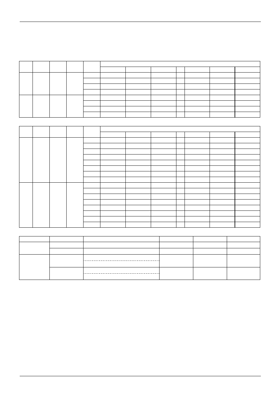
7.2.3
Connection examples of plural segment drivers
(c) When L/R = "L"
(d) When L/R = "H"
Y
160
Y
160
Y
160
Y
1
Y
1
Y
1
EIO2
EIO2
EIO2
EIO1
EIO1
EIO1
XCK
LP
MD
FR
DI
7
-DI
0
XCK
LP
MD
FR
DI
7
-D
I
0
L/R
L/R
L/R
V
DD
8
Top data
Last data
Data flow
XCK
LP
MD
FR
DI
7
-D
I
0
XCK
LP
MD
FR
DI
7
-D
I
0
V
ss
Y
160
Y
160
Y
160
Y
1
Y
1
Y
1
EIO2
EIO2
EIO2
EIO1
EIO1
EIO1
XCK
LP
MD
FR
DI
7
-DI
0
XCK
LP
MD
FR
DI
7
-D
I
0
XCK
LP
MD
FR
DI
7
-D
I
0
XCK
LP
MD
FR
DI
7
-D
I
0
L/R
L/R
L/R
V
SS
8
Top data
Last data
Data flow
Sitronix ST8016
V1.0 11/26
2003-07-02
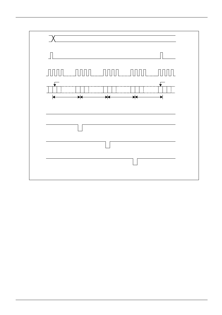
7.2.4
Timing chart of 4-device cascade connection of segment drivers
n*
n*
n*
n*
n*
1
1
1
1
1
2
2
2
2
2
device A
device B
device C
device D
TOP DATA
LAST DATA
*n = 40 in 4-bit parallel input mode
*n = 20 in 8-bit parallel input mode
EO
(device C)
EO
(device B)
EO
(device A)
EI
(device A)
DI7 - DI0
XCK
LP
FR

Sitronix ST8016
V1.0 12/26
2003-07-02
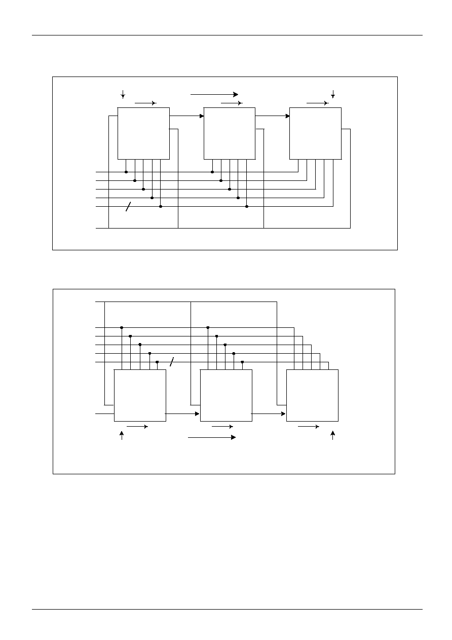
7.2.5
Connection examples for plural common drivers
(e) Single Mode (L/R = "L")
Y
160
Y
160
Y
160
Y
1
Y
1
Y
1
EIO2
EIO2
EIO2
EIO1
EIO1
EIO1
LP
V
SS
FR
DISPOFF
L/R
LP
MD
FR
DI
7
V
SS
(V
DD
)
First
Last
FLM
DI
SPO
F
F
L/R
LP
MD
FR
DI
7
DI
SPO
F
F
L/R
LP
MD
FR
DI
7
DI
SPO
F
F
(f)
Single Mode (L/R = "H")
Y
160
Y
160
Y
160
Y
1
Y
1
Y
1
EIO2
EIO2
EIO2
EIO1
EIO1
EIO1
FR
L/R
DI
SPO
F
F
MD
FR
DI
7
LP
DISPOFF
V
SS
(V
DD
)
First
Last
LP
V
SS
V
DD
FLM
L/R
DI
SPO
F
F
MD
FR
DI
7
LP
L/R
DI
SPO
F
F
MD
FR
DI
7
LP
Sitronix ST8016
V1.0 13/26
2003-07-02
(g) Dual Mode (L/R = "L")
Y
160
Y
160
Y
160
Y
1
Y
1
Y
1
EIO2
EIO2
EIO2
EIO1
EIO1
EIO1
LP
V
SS
FR
DISPOFF
L/R
LP
MD
FR
DI
7
V
SS
(V
DD
)
First
Last 2
FLM1
DI
SPO
F
F
L/R
LP
MD
FR
DI
7
DI
SPO
F
F
L/R
LP
MD
FR
DI
7
DI
SPO
F
F
First 2
Last 1
Y
81
Y
80
FLM2
V
DD
(h) Dual mode (L/R = "H")
Y
160
Y
160
Y
160
Y
1
Y
1
Y
1
EIO2
EIO2
EIO2
EIO1
EIO1
EIO1
FR
L/R
DI
SPO
F
F
MD
FR
DI
7
LP
DISPOFF
V
SS
(V
DD
)
First 1
Last 2
LP
V
SS
V
DD
FLM1
L/R
DI
SPO
F
F
MD
FR
DI
7
LP
L/R
DI
SPO
F
F
MD
FR
DI
7
LP
Last 1 First 2
Y
80
Y
81
FLM2
Sitronix ST8016
V1.0 14/26
2003-07-02
8. PRECAUTIONS
Precautions when connecting or disconnecting the
power supply
This IC has a high-voltage LCD driver, so a high
current that may flow if voltage is supplied to the LCD
drive power supply while the logic system power
supply is floating may permanently damage it. The
details are as follows,
When connecting the power supply, connect the LCD
drive power after connecting the logic system power.
Furthermore, when disconnecting the power,
disconnect the logic system power after
disconnecting the LCD drive power
It is advisable to connect the serial resistor (50 to
100 ) or fuse to the LCD drive power V
0
of the
system as a current limiter. Set up a suitable value of
the resistor in consideration of the display grade.
And when connecting the logic power supply, the logic
condition of this IC inside is insecure. Therefore
connect the LCD drive power supply after resetting
logic condition of this IC inside on /DISPOFF function.
After that, cancel the /DISPOFF function after the LCD
drive power supply has become stable. Furthermore,
when disconnecting the power, set the LCD drive
output pins to level Vss on /DISPOFF function. Then
disconnect the logic system power after disconnecting
the LCD drive power.
When connecting the power supply, follow the
recommended sequence shown here
.
V
DD
V
SS
V
DD
V
SS
V
DD
V
SS
V
DD
DISPOFF
V
0
Sitronix ST8016
V1.0 15/26
2003-07-02
9. ABSOLUTE MAXIMUM RATINGS
PARAMETER
SYMBOL
APPLICABLE PINS
RATING
UNIT
NOTE
Supply voltage (1)
V
DD
V
DD
-0.3~ +7.0
V
V
0
V
0L
, V
0R
-0.3 ~ +45.0
V
V
12
V
12L
, V
12R
V
0
-10~ V
0
+ 0.3
V
Supply voltage (2)
V
43
V
43L
, V
43R
-0.3 ~ V
SS
+ 10
V
Input voltage
V
I
D1
7
-DI
0
, XCK, LP, L/R, FR,
MD, S/C, EIO
1
, EIO
2
,
/DISPOFF, TEST
1
-0.3 to V
DD
+ 0.3
V
1,2
Storage temperature
T
STG
-45
to
+125
∞C
NOTES:
1. TA = +25 ∞C
2. The maximum applicable voltage on any pin with respect to V
SS
(0 V).
10. RECOMMENDED OPERATING CONDITIONS
PARAMETER SYMBOL
APPLICABLE
PINS
MIN.
TYP.
MAX.
UNIT NOTE
Supply voltage (1)
V
DD
V
DD
+2.5
+5.5
V
Supply voltage (2)
V
0
V
0L
, V
0R
+15.0
+40.0
V
1, 2
Operating temperature
T
OPR
-25
+85
∞
C
NOTES:
1. The applicable voltage on any pin with respect to V
SS
(0 V).
2. Ensure that voltages are set such that V
SS
< V
43
< V
l2
< V
0
.
Sitronix ST8016
V1.0 16/26
2003-07-02
11. ELECTRICAL CHARACTERISTICS
11.1 DC
Characteristics
(Segment Mode)
(V
SS
= 0 V, V
DD
= +2.5 to +5.5 V, V
0
= + 15.0 to +30.0 V, T
OPR
= -25 to +85∞C)
PARAMETER SYMBOL CONDITIONS
APPLICABLE
PINS MIN.
TYP.
MAX.
UNIT NOTE
Input "Low" voltage
V
IL
0.2V
DD
V
Input "High" voltage
V
IH
DI
7
-DI
0
, XCK, LP, L/R
FR, MD, S/C, EIO
1
, EIO
2
,
/DISPOFF
0.8V
DD
V
Output "Low" voltage
V
OL
I
OL
= +0.4 mA
+0.4
V
Output "High" voltage
V
OH
I
OH
= -0.4 mA
EIO
1
, EIO
2
V
DD
-0.4
V
I
LIL
V
I
= V
SS
-10
µA
Input leakage current
I
LIH
V
I
= V
DD
DI
7
-DI
0
, XCK, LP, LIR,
FR, MD, S/C, EIO
1
, EIO
2
,
/DISPOFF
+10 µA
Output resistance
R
ON
|V
ON
|
=0.5V
V
0
= 30 V
Y
1
-Y
160
1.0 1.5 k
Standby current
I
STB
V
SS
50
µA
1
Supply current (1)
(Non-selection)
I
DD1
V
DD
2.0 mA
2
Supply current (2)
(Selection)
I
DD2
V
DD
7.0 mA
3
Supply current (3)
I
0
V
0L
, V
0R
0.9
mA
4
NOTES:
1. V
DD
= +5.0 V, V
0
= +30.0 V, Vi = V
SS
.
2. V
DD
= +5.0 V, V
0
= +30.0 V, f
XCK
= 8 MHz, no-load, El = V
DD
. The input data is turned over by data taking clock
(4-bit parallel input mode).
3. V
DD
= +5.0 V, V
0
= +30.0 V, f
XCK
= 8 MHz, no-load, El = V
SS
. The input data is turned over by data taking clock
(4-bit parallel input mode).
4. V
DD
= +5.0 V, V
0
= +30.0 V, f
XCK
= 8MHz, f
LP
= 19.2 kHz, f
FR
= 80 Hz, no-load. The input data is turned over by
data taking clock (4-bit parallel input mode).
(Common Mode) (V
SS
= 0 V, V
DD
= +2.5 to +5.5 V, V
0
= + 15.0 to +30.0 V, T
OPR
= -25 to +85 ∞C)
PARAMETER SYMBOL
CONDITIONS
APPLICABL
E
PINS MIN.
TYP.
MAX.
UNIT NOTE
Input "Low" voltage
V
IL
0.2V
DD
V
Input "High" voltage
V
IH
DI
7
-DI
0
, XCK, LP, L/R
FR, MD, S/C, EIO
1
,
EIO
2
, /DISPOFF
0.8V
DD
V
Output "Low" voltage
V
OL
I
OL
= +0.4 mA
+0.4
V
Output "High" voltage
V
OH
I
OH
= -0.4 mA
EIO
1
, EIO
2
V
DD
-0.4
V
I
LIL
V
I
= V
SS
DI
7
-DI
0
, XCK, LP,
LIR, FR, MD, S/C,
EIO
1
, EIO
2
,
/DISPOFF
-10.0 µA
Input leakage current
I
LIH
V
I
= V
DD
DI
6
-DI
0
, LP, L/R, FR,
MD, S/C, /DISPOFF
+10.0 µA
Input pull-down current
I
PD
V
I
= V
DD
DI
7
, XCK, EIO
1
, EIO
2
100
µA
Output resistance
R
ON
|V
ON
|
=0.5V
V
0
= 30 V
Y
1
-Y
160
1.0 1.5 k
Standby current
I
SPD
V
SS
50
µA
1
Supply current (1)
I
DD
V
DD
80
µA
2
Supply current (2)
I
0
V
OL
, V
OR
130
µA
2
NOTES:
1. V
DD
= +5.0 V, V
0
= +30.0 V, V
I
= V
SS
2. V
DD
= +5.0 V, V
0
= +30.0 V, f
LP
=19.2 kHz, f
FR
= 80 Hz, 1/240 duty operation, no-load.
Sitronix ST8016
V1.0 17/26
2003-07-02
11.2 AC
Characteristics
(Segment Mode 1)
(V
SS
= 0 V, V
DD
= +2.5 to +3.0 V, V
0
= + 15.0 to +30.0 V, T
OPR
= -25 10+85 ∞C)
PARAMETER SYMBOL
CONDITIONS
MIN
TYP.
MAX.
UNIT
NOTE
Shift clock period
t
WCK
t
R
,t
F
11ns
125
ns
1
Shift clock "H" pulse width
t
WCKH
51
ns
Shift clock "L" pulse width
t
WCKL
51
ns
Data setup time
t
DS
30
ns
Data hold time
t
DH
40
ns
Latch pulse "H" pulse width
t
WLPH
51
ns
Shift clock rise to latch pulse rise time
t
LD
0
ns
Shift clock fall to latch pulse fall time
t
SL
51
ns
Latch pulse rise to shift clock rise time
t
LS
51
ns
Latch pulse fall to shift clock fall time
t
LH
51
ns
Enable setup time
t
S
36
ns
Input signal rise time
t
R
50
ns
2
Input signal fall time
t
F
50
ns
2
DISPOFF removal time
t
SD
100
ns
DISPOFF "L" pulse width
t
WDL
1.2
µs
Output delay time (1)
t
D
CL = 15 pF
78
ns
Output delay time (2)
t
PD1
, t
PD2
CL = 15 pF
1.2
µs
Output delay time (3)
t
PD3
CL = 15 pF
1.2
µs
NOTES:
1. Takes the cascade connection into consideration.
2. (t
WCK
- t
WCKH
- t
WCKL
)/2 is maximum in the case of high speed operation.
(Segment Mode 2) (V
SS
= 0 V, V
DD
= +5.0±0.5 V, V
0
= + 15.0 to +30.0 V, T
OPR
= -25 to +85 ∞C)
PARAMETER SYMBOL
CONDITIONS
MIN.
TYP.
MAX.
UNIT
NOTE
Shift clock period
t
WCK
t
R
,t
F
10ns
66
ns
1
Shift clock "H" pulse width
t
WCKH
23
ns
Shift clock "L" pulse width
t
WCKL
23
ns
Data setup time
t
DS
15
ns
Data hold time
t
DH
23
ns
Latch pulse "H" pulse width
t
WLPH
30
ns
Shift clock rise to latch pulse rise time
t
LD
0
ns
Shift clock fall to latch pulse fall time
t
SL
50
ns
Latch pulse rise to shift clock rise time
t
LS
30
ns
Latch pulse fall to shift clock fall time
t
LH
30
ns
Enable setup time
t
S
15
ns
Input signal rise time
t
R
50 ns
2
Input signal fall time
t
F
50 ns
2
DISPOFF removal time
t
SD
100
ns
DISPOFF "L" pulse width
t
WDL
1.2
µs
Output delay time (1)
t
D
CL = 15 pF
41
ns
Output delay time (2)
t
PD1
, t
PD2
CL = 15 pF
1.2
µs
Output delay time (3)
t
PD3
CL = 15 pF
1.2
µs
NOTES:
1. Takes the cascade connection into consideration.
2. (t
WCK
- t
WCKH
- t
WCKL
)/2 is maximum in the case of high speed operation.
Sitronix ST8016
V1.0 18/26
2003-07-02
(Segment Mode 3) (V
SS
= 0 V, V
DD
= +3.0 to +4.5 V, V
0
= + 15.0 to +30.0 V, T
OPR
= -25 10+85 ∞C)
PARAMETER SYMBOL
CONDITIONS
MIN.
TYP.
MAX.
UNIT
NOTE
Shift clock period
t
WCK
t
R
,t
F
10ns
82
ns
1
Shift clock "H" pulse width
t
WCKH
28
ns
Shift clock "L" pulse width
t
WCKL
28
ns
Data setup time
t
DS
20
ns
Data hold time
t
DH
23
ns
Latch pulse "H" pulse width
t
WLPH
30
ns
Shift clock rise to latch pulse rise time
t
LD
0
ns
Shift clock fall to latch pulse fall time
t
SL
51
ns
Latch pulse rise to shift clock rise time
t
LS
30
ns
Latch pulse fall to shift clock fall time
t
LH
30
ns
Enable setup time
t
S
15
ns
Input signal rise time
t
R
50 ns
2
Input signal fall time
t
F
50 ns
2
DISPOFF removal time
t
SD
100
ns
DISPOFF "L" pulse width
t
WDL
1.2
µs
Output delay time (1)
t
D
CL = 15 pF
57
ns
Output delay time (2)
t
PD1
, t
PD2
CL = 15 pF
1.2
µs
Output delay time (3)
t
PD3
CL = 15 pF
1.2
µs
NOTES:
1. Takes the cascade connection into consideration.
2. (t
WCK
- t
WCKH
- t
WCKL
)/2 is maximum in the case of high speed operation.
(Common Mode)
(V
SS
= 0 V, V
DD
= +2.5 to +5.5 V, V
0
= + 15.0 to +30.0 V, T
OPR
= -25 10+85 ∞C)
PARAMETER SYMBOL
CONDITIONS
MIN
TYP
MAX UNIT
Shift clock period
t
WLP
t
R
, t
F
20ns 250
ns
Shift clock "H" pulse width
t
WLPH
V
DD
=5± 0.5V
V
DD
=2.5~4.5V
15
30
ns
Data setup time
t
SU
30
ns
Data hold time
t
H
50
ns
Input signal rise time
t
R
50
ns
Input signal fall time
t
F
50
ns
DISPOFF removal time
t
SD
100
ns
DISPOFF "L" pulse width
t
WDL
1.2
us
Output delay time (1)
t
DL
CL=10pF
200
ns
Output delay time (2)
t
PD1
,t
PD2
CL=10pF
1.2
us
Output delay time (3)
t
PD3
CL=10pF
1.2
us
Sitronix ST8016
V1.0 19/26
2003-07-02
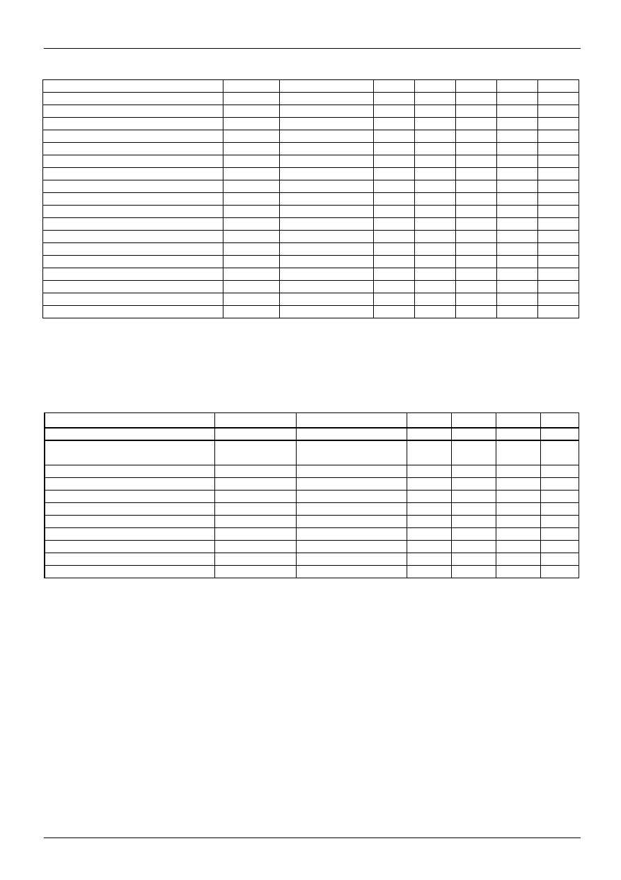
11.3 Timing Chart of Segment Mode
t
S
1
2
n*
t
D
LP
XCK
EI
EO
*n = 40 in 4-bit parallel input mode
*n = 20 in 8-bit parallel input mode
LP
XCK
DI7 - DI0
DISPOFF
t
WLPH
t
LD
t
SL
t
LH
t
LS
t
WCKH
t
F
t
R
t
WCK
t
DS
t
DH
TOP DATA
LAST DATA
t
WDL
t
SD
t
WCKL
Sitronix ST8016
V1.0 20/26
2003-07-02
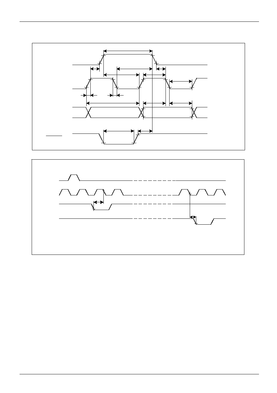
FR
LP
DISPOFF
Y
1
- Y
160
t
PD1
t
PD3
t
PD2
Fig. 8 Timing Characteristics (3)
(Common Mode)
(V
SS
= 0 V, V
DD
= +2.5 to +5.5 V, V
0
= +15.0 to +30.0 V, T
OPR
= -25 to +85∞ C)
PARAMETER SYMBOL
CONDITIONS
MIN.
TYP.
MAX.
UNIT
Shift clock period
t
WLP
t
R
,t
F
20ns
250
ns
V
DD
= +5.0± 0.5V
15
ns
Shift clock "H" pulse width
t
WLPH
V
DD
= +2.5+ 4.5V
30
ns
Data setup time
t
SU
30
ns
Data hold time
t
H
50
ns
Input signal rise time
t
R
50 ns
Input signal fall time
t
F
50 ns
DISPOFF removal time
t
SD
100
ns
DISPOFF "L" pulse width
t
WDL
1.2
µs
Output delay time (1)
t
DL
CL = 15 pF
200
ns
Output delay time (2)
t
PD1
, t
PD2
CL = 15 pF
1.2
µs
Output delay time (3)
t
PD3
CL = 15 pF
1.2
µs

Sitronix ST8016
V1.0 21/26
2003-07-02
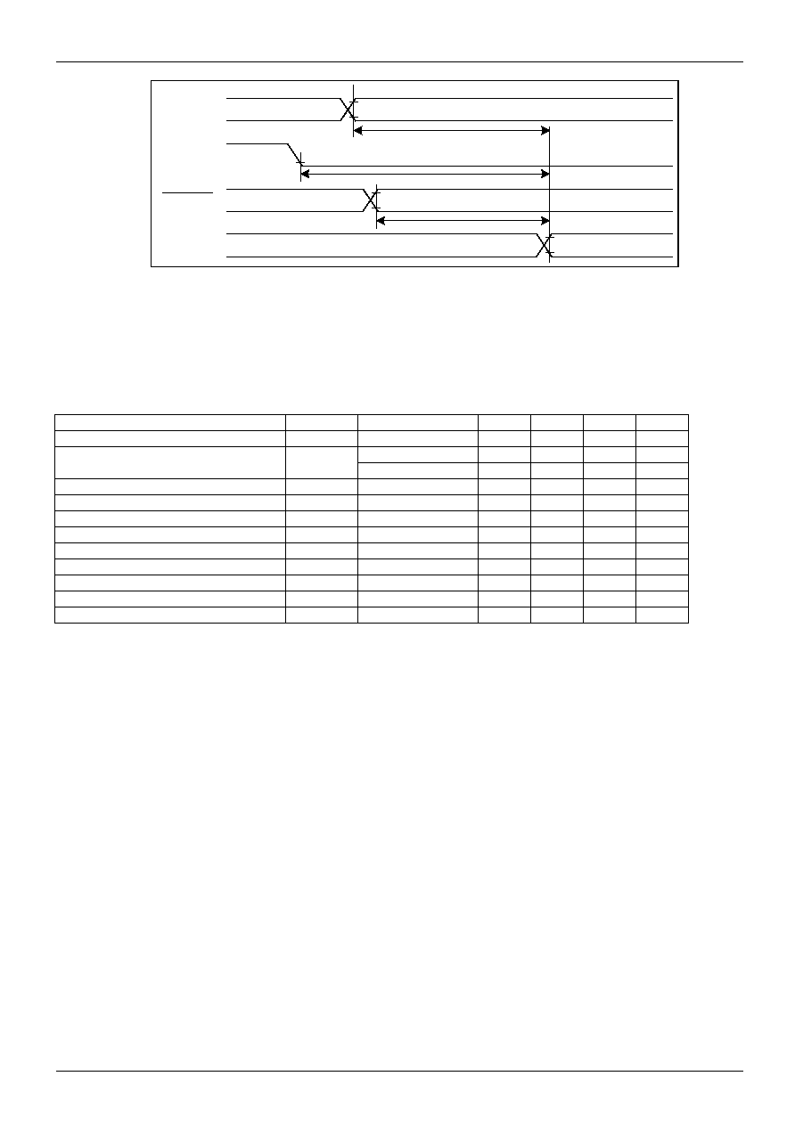
11.4
Timing Chart of Common Mode
LP
EIO
2
EIO
1
DISPOFF
t
WDL
t
SD
t
DL
t
H
t
SU
t
WLP
t
R
t
WLPH
t
F
FR
LP
Y
1
- Y
160
t
PD1
t
PD3
t
PD2
DISPOFF
Sitronix ST8016
V1.0 22/26
2003-07-02
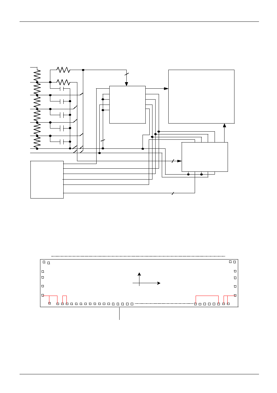
12. APPLICATION CIRCUIT
12.1
Application Circuit for Module
160 X 160 DOT LCD PANEL
FR
LP
/DISPOFF
/XCK
FR
LP
/D
IS
P
O
F
F
/X
C
K
EIO
1
MD
S/C
L/R
EIO
2
DI
0
~DI
7
V
EE
V
4
V
3
V
2
V
1
V
0
V
SS
V
DD
5
EI
O
1
MD
S/
C
L/
R
EI
O
2
DI
0
~D
I
7
FLM
LP
/DISPOFF
/XCK
AC
XD
0
~XD
7
CONTROLLER
50~100 ohm
5
8
8
Y1~Y160
Y
1
~Y
160
ST8016
ST8016
12.2
Application Circuit for COG Layout ( Example )
D
U
MMY
D
U
MMY
D
U
MMY
D
U
MMY
OP
T
ION_V
DD
Y
160
198
D
U
MMY
_P
A
D
V
0
199
LR
1
202
203
GND
V
SS
V
DD
2
S/
C
3
EI
O
2
4
DI0
5 6
7 8
DI1
DI2
DI3
DI4
9 10 11 12
DI5
DI6
DI7
13 14
XCK
DI
SPO
F
F
V
43
V
12
201
200
V
SS
33
D
U
MMY
_P
A
D
37
Y
0
X
Y
Chip size = 10000 um x 1040 um
subtrate connect to ground
(0,0)
ST8016
V
43
V
12
V
0
34
35
36
32
GND
GND
ST8016
LP
28 29
EI
O
1
FR
MD
31
30
27
15 16 17
25 26
Sitronix ST8016
V1.0 23/26
2003-07-02
13. PAD DIAGRAM
LR
1
32
GND
GND
V
SS
33
D
U
MMY
_P
A
Y
160
37
Y
0
198
D
U
MMY
_P
A
202
203
GND
X
Y
Chip size = 10000 um x 1040 um
subtrate connect to ground
(0,0)
ST8016
V
SS
ST8016
V
DD
2
S/
C
3
EI
O
2
4
DI0
5 6
7 8
DI1
DI2
DI3
DI4
9 10 11 12
DI5
DI6
DI7
13 14
XCK
DI
SPO
F
F
LP
28 29
EI
O
1
FR
MD
31
30
27
V
43
V
12
V
0
201
200
199
V
43
V
12
V
0
34
35
36
Unit: um
PIN#
Name X Y
PIN#
Name X Y
1
L/R
-4538.6 -406.9 34
V34
4904.5 -125.7
2 VDD -4227.0
-409.7
35 V12 4904.5
90.7
3 S/C -4074.5
-406.9
36 V0 4904.5
265.9
4 EIO2 -3607.4
-406.9
37
DUMMY_PAD
4890.0
438.3
5 DI0 -3413.4
-406.9
38 Y1 4770.0
383.8
6 DI1 -3056.4
-406.9
39 Y2 4710.0
383.8
7 DI2 -2862.4
-406.9
40 Y3 4650.0
383.8
8 DI3 -2505.9
-406.9
41 Y4 4590.0
383.8
9 DI4 -2311.9
-406.9
42 Y5 4530.0
383.8
10 DI5 -1955.6
-406.9
43 Y6 4470.0
383.8
11 DI6 -1761.6
-406.9
44 Y7 4410.0
383.8
12 DI7 -1355.9
-406.9
45 Y8 4350.0
383.8
13 XCK -1161.9
-406.9
46 Y9 4290.0
383.8
14 DISPOFFB -741.5
-406.9
47
Y10
4230.0 383.8
15 DUMMY_PAD -586.0 -419.2 48
Y11
4170.0 383.8
16 DUMMY_PAD -70.4 -421.5 49
Y12
4110.0 383.8
17 DUMMY_PAD 152.5 -398.3 50
Y13
4050.0 383.8
18 DUMMY_PAD 400.6 -394.3 51
Y14
3990.0 383.8
19 DUMMY_PAD 768.3 -398.7 52
Y15
3930.0 383.8
20 DUMMY_PAD 1183.9 -398.7 53
Y16
3870.0 383.8
21 DUMMY_PAD 1474.6 -395.3 54
Y17
3810.0 383.8
22 DUMMY_PAD 1595.8 -411.9 55
Y18
3750.0 383.8
23 DUMMY_PAD 2092.5 -412.6 56
Y19
3690.0 383.8
24 DUMMY_PAD 2318.2 -404.5 57
Y20
3630.0 383.8
25 OPTION_VDD 2744.0 -407.1 58
Y21
3570.0 383.8
26 DUMMY_PAD 3082.8 -407.1 59
Y22
3510.0 383.8
27 LP 3220.8
-406.9
60 Y23 3450.0
383.8
28 EIO1 3701.6
-406.9
61 Y24 3390.0
383.8
29 FR 3895.6
-406.9
62 Y25 3330.0
383.8
30 MD 4313.0
-406.9
63 Y26 3270.0
383.8
31 GND 4525.0
-406.9
64 Y27 3210.0
383.8
32 GND 4720.4
-404.3
65 Y28 3150.0
383.8
33 V5 4904.5
-344.1
66 Y29 3090.0
383.8
Sitronix ST8016
V1.0 24/26
2003-07-02
67
Y30
3030.0 383.8
118
Y81
-30.0 383.8
68
Y31
2970.0 383.8
119
Y82
-90.0 383.8
69
Y32
2910.0 383.8
120
Y83
-150.0 383.8
70
Y33
2850.0 383.8
121
Y84
-210.0 383.8
71
Y34
2790.0 383.8
122
Y85
-270.0 383.8
72
Y35
2730.0 383.8
123
Y86
-330.0 383.8
73
Y36
2670.0 383.8
124
Y87
-390.0 383.8
74
Y37
2610.0 383.8
125
Y88
-450.0 383.8
75
Y38
2550.0 383.8
126
Y89
-510.0 383.8
76
Y39
2490.0 383.8
127
Y90
-570.0 383.8
77
Y40
2430.0 383.8
128
Y91
-630.0 383.8
78
Y41
2370.0 383.8
129
Y92
-690.0 383.8
79
Y42
2310.0 383.8
130
Y93
-750.0 383.8
80
Y43
2250.0 383.8
131
Y94
-810.0 383.8
81
Y44
2190.0 383.8
132
Y95
-870.0 383.8
82
Y45
2130.0 383.8
133
Y96
-930.0 383.8
83
Y46
2070.0 383.8
134
Y97
-990.0 383.8
84
Y47
2010.0 383.8
135
Y98
-1050.0 383.8
85
Y48
1950.0 383.8
136
Y99
-1110.0 383.8
86
Y49
1890.0 383.8
137
Y100
-1170.0 383.8
87
Y50
1830.0 383.8
138
Y101
-1230.0 383.8
88
Y51
1770.0 383.8
139
Y102
-1290.0 383.8
89
Y52
1710.0 383.8
140
Y103
-1350.0 383.8
90
Y53
1650.0 383.8
141
Y104
-1410.0 383.8
91
Y54
1590.0 383.8
142
Y105
-1470.0 383.8
92
Y55
1530.0 383.8
143
Y106
-1530.0 383.8
93
Y56
1470.0 383.8
144
Y107
-1590.0 383.8
94
Y57
1410.0 383.8
145
Y108
-1650.0 383.8
95
Y58
1350.0 383.8
146
Y109
-1710.0 383.8
96 Y59 1290.0
383.8
147 Y110 -1770.0
383.8
97
Y60
1230.0 383.8
148
Y111
-1830.0 383.8
98 Y61 1170.0
383.8
149 Y112 -1890.0
383.8
99 Y62 1110.0
383.8
150 Y113 -1950.0
383.8
100 Y63 1050.0
383.8
151 Y114 -2010.0
383.8
101 Y64
990.0
383.8
152 Y115 -2070.0
383.8
102 Y65
930.0
383.8
153 Y116 -2130.0
383.8
103 Y66
870.0
383.8
154 Y117 -2190.0
383.8
104 Y67
810.0
383.8
155 Y118 -2250.0
383.8
105 Y68
750.0
383.8
156 Y119 -2310.0
383.8
106
Y69
690.0 383.8
157
Y120
-2370.0 383.8
107
Y70
630.0 383.8
158
Y121
-2430.0 383.8
108
Y71
570.0 383.8
159
Y122
-2490.0 383.8
109
Y72
510.0 383.8
160
Y123
-2550.0 383.8
110
Y73
450.0 383.8
161
Y124
-2610.0 383.8
111
Y74
390.0 383.8
162
Y125
-2670.0 383.8
112
Y75
330.0 383.8
163
Y126
-2730.0 383.8
113
Y76
270.0 383.8
164
Y127
-2790.0 383.8
114
Y77
210.0 383.8
165
Y128
-2850.0 383.8
115
Y78
150.0 383.8
166
Y129
-2910.0 383.8
116
Y79
90.0 383.8
167
Y130
-2970.0 383.8
117
Y80
30.0 383.8
168
Y131
-3030.0 383.8
Sitronix ST8016
V1.0 25/26
2003-07-02
169 Y132 -3090.0
383.8
187 Y150 -4170.0
383.8
170 Y133 -3150.0
383.8
188 Y151 -4230.0
383.8
171 Y134 -3210.0
383.8
189 Y152 -4290.0
383.8
172 Y135 -3270.0
383.8
190 Y153 -4350.0
383.8
173 Y136 -3330.0
383.8
191 Y154 -4410.0
383.8
174 Y137 -3390.0
383.8
192 Y155 -4470.0
383.8
175 Y138 -3450.0
383.8
193 Y156 -4530.0
383.8
176 Y139 -3510.0
383.8
194 Y157 -4590.0
383.8
177 Y140 -3570.0
383.8
195 Y158 -4650.0
383.8
178 Y141 -3630.0
383.8
196 Y159 -4710.0
383.8
179 Y142 -3690.0
383.8
197 Y160 -4770.0
383.8
180 Y143 -3750.0
383.8
198
DUMMY_PAD -4890.0
438.3
181 Y144 -3810.0
383.8
199 V0 -4904.5
265.9
182 Y145 -3870.0
383.8
200 V12 -4904.5
90.7
183 Y146 -3930.0
383.8
201 V34 -4904.5
-125.7
184 Y147 -3990.0
383.8
202 V5 -4904.5
-344.1
185 Y148 -4050.0
383.8
203 GND -4781.8
-404.9
186 Y149 -4110.0
383.8
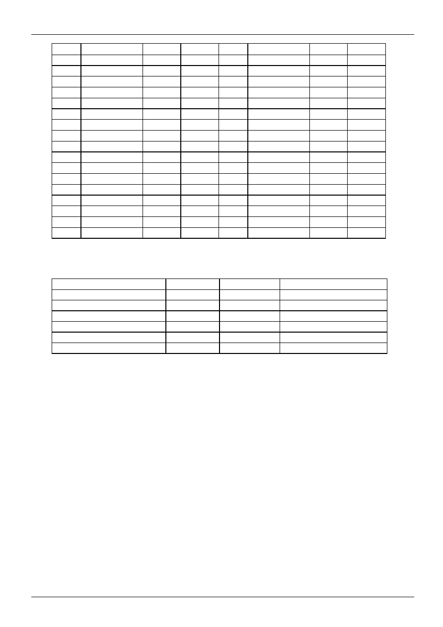
13.1
Gold Bump size (unit: um)
Pad No.
X
Y
Area (um
2
)
38~197 45
72
3240
1~14,17,27~31 60
60
5100
33~36,199~202 58
62 3596
15,16,18,21~26 38
60 2280
19,20 60
38
2280
37,198,32,203 85
60
5100
Bump pad height (pad 1~198) = 18um, strength=30g

Sitronix ST8016
V1.0 26/26
2003-07-02
Appendix:
2000-May-16............................ Page1, modify pin configuration
2000-Jul-25.............................. Application circuit
2000-Aug-1.............................. Pad allocation, Bump size
2000-Aug-9(version0.14) ......... change pad name V5 as Vss
2000-Aug-17(version 0.143) .... add pad 203 gold bump data
2000-Oct-9(version 0.152)....... add some bump information
2000-Nov-2(version 0.153) ...... correct pad name
2000/Dec/4(version0.16).......... update TCP(F18) information
2000/Dec/19(version 0.17)....... correct all V5 as Vss
2000/Dec/26(version 0.2)......... AC/DC data revise
2001/Feb/8(0.23) ..................... correct segment mode MD=L/H=4/8 bit (section 7.2.2)
2001/Mar/1(0.24) ..................... gold bump strength=30g
2001/May/22(0.30).................Dual mode describe correct and COG application circuit (section 12.2)
2001/June/11(0.31)................Correct some wrong word mistake
2001/Aug/29(0.32).................add Input/Output circuit
2001/Sep/28(0.33).................t
SL
MIN change to 51 , and change parameter name
2001/Oct/4(0.34)...................Correct AC characteristics column
2002/Jun/07(0.35)..................Change operating temperature from -20∞C~85∞C to -25∞C~85∞C
2003/7/2(1.0)........................Change 1~14,17,27~32,203 Gold Bump size