
ST
Sitronix
ST8600
PRELIMINARY
240 Channel Common Driver for STN LCD with High-Voltage Drive
Notice: This is not a final specification. Some parameters are subject to change
Ver 0.2
1/18
2001/Feb/28
1
1
F
F
e
e
a
a
t
t
u
u
r
r
e
e
s
s
Duty cycle up to 1/240
LCD drive voltage: 43V max
Built-in switching circuit (generate �21.5V)
240 LCD drive circuits
Operating voltage: 2.5 to 5.5 V
Intermediate voltage I/F
Built-in alternating signal generating circuit Pin
programmable
160/200/240 output mode
Display-off function
2
2
D
D
e
e
s
s
c
c
r
r
i
i
p
p
t
t
i
i
o
o
n
n
The ST8600 is a 240-channel common driver that drives a
dot matrix LCD panel. By changing the mode, this can be
applied to 240,200 and 160 channel output. Through the
use of a 43V high voltage CMOS process technology, a
high voltage drive of +21.5V, centering on VM is
possible. �21.5V generated from +21.5V with built-in
switching circuit and external capacity. Low logic drive
voltage is used. This device is used together with the
segment drive ST8624, ST8632 or ST8640.
Sitronix ST8600
Ver 0.2
2/18
2001/Feb/28
3
3
P
P
i
i
n
n
a
a
s
s
s
s
i
i
g
g
n
n
m
m
e
e
n
n
t
t
(
(
T
T
C
C
P
P
)
)
C1
C2
DIO2
M
RESET
MWS4
MWS3
MWS1
MWS2
VCC
MWS0
MODE0
MODE1
DISPOFF
DOC
AMP
SHL
GND
CL
CCL
M/S
DIO1
VEER
VLR
VMR
VHR
VLCDR
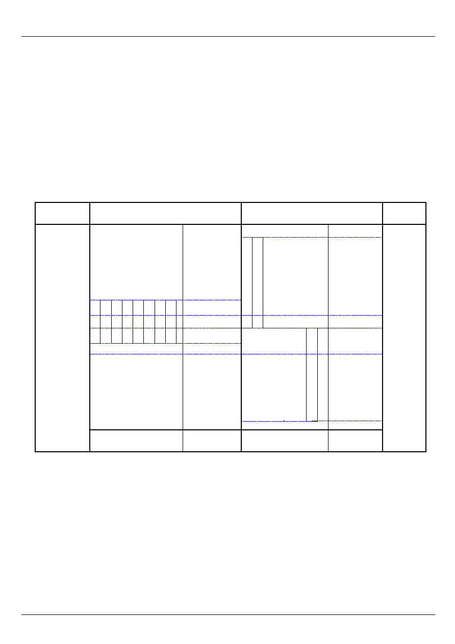
Top view
X1
X2
X3
X4
X237
X238
X239
X240
267
266
265
264
263
262
261
259
260
257
258
255
256
253
254
252
251
250
249
248
247
246
245
244
243
242
241
1
2
3
4
237
238
239
240
Figure 1 ST8600 TCP pin assignment
VLCDL
VHL
VML
VLL
VEEL
VEO
273
272
271
270
269
268
Sitronix ST8600
Ver 0.2
3/18
2001/Feb/28
4
4
B
B
l
l
o
o
c
c
k
k
D
D
i
i
a
a
g
g
r
r
a
a
m
m
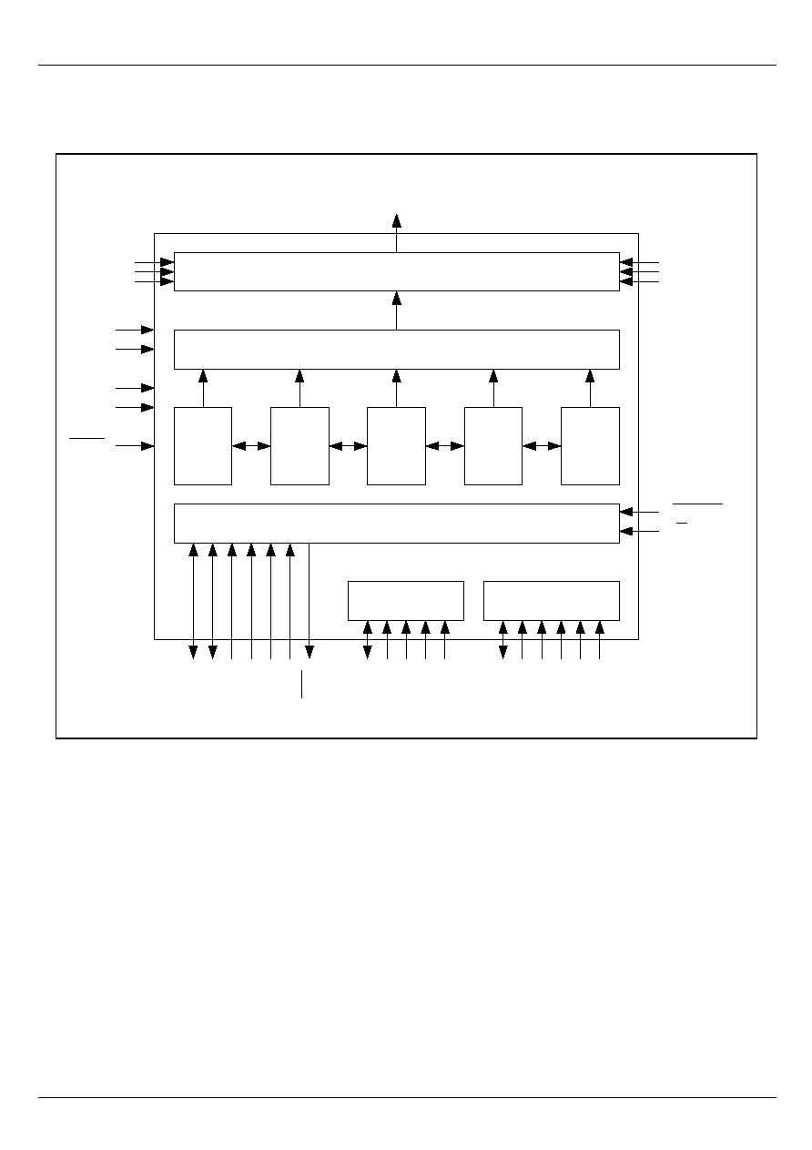
shift
register
1~20
shift
register
21~40
shift
register
41~200
shift
register
201~220
shift
register
221~240
logic
switching circuit
alternating signal
generating circuit
level shifter
LCD drive
MWS2
MWS3
MWS0
MWS1
MWS4
M
DIO1
DIO2
SHL
MODE0
MODE1
CL
VEO
CCL
AMP
C2
C1
X1~X240
VHL
VLL
VML
VHR
VLR
VMR
VLCDL,R
VEEL,R
Vdd
GND
RESET
DOC
DISPOFF
M/S

Sitronix ST8600
Ver 0.2
4/18
2001/Feb/28
5
5
B
B
l
l
o
o
c
c
k
k
F
F
u
u
n
n
c
c
t
t
i
i
o
o
n
n
s
s
LCD Drive Circuit
This circuit selects and output the three level signals for
the LCD drive. By a combination of the data in the shift
register and M, either VH, VL or VM is selected and
transmitted to the output circuit.
Level shifter
This boosts a 5V signal to a high voltage signal for LCD
drive.
Shift register
This is a 240-bit bi-directional shift register circuit. The first
line marker signal output from the DIO1 pin and DIO2 pin
is sequentially shifted by shift clock CL. The SHL pin
determines the shift direction.
Alternation signal generating circuit
This circuit generates an alternating signal (M signal) for
LCD display. To suppress cross talk, the signal is
alternated in a unit from several lines to several tens of
lines. By connecting MWS0~MWS4 pins to Vdd or GND,
the desired number of signals can be alternated. When
alternating are externally input, all pins (MWS0 ~ MWS4)
are connected to GND.
Sitronix ST8600
Ver 0.2
5/18
2001/Feb/28
6
6
P
P
i
i
n
n
D
D
e
e
s
s
c
c
r
r
i
i
p
p
t
t
i
i
o
o
n
n
(
(
T
T
C
C
P
P
)
)
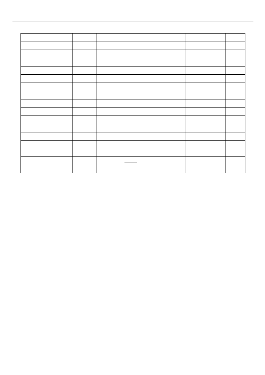
PIN NO.
SYMBOL
I/O
DESCRIPTION
1~240 X1~X240
O
Either level VH, VL or VM is output according to the combination of the M signal and
display data when the DISP pin is set at Vdd. See figure 3
272, 242
271, 243
270, 244
273, 241
269, 245
VHL, VHR
VML, VMR
VLL, VLR
VLCDL, VLCDR
VEEL, VEER
P
LCD drive-level voltage.
VHL, VHR, VLL, VLR: selected level. VML, VMR: non-selected level
257, 250
Vdd, GND
P Logic power supply
268 VEO
P When the built-in switching circuit and generate VEE, VEO pin connect to VEEL, R
pins. VM voltage is point of reference and reversed and output the voltage input to
the voltage between VLCD and VM. If built-in switching circuit is not used, don't
connect any lines to this pin.
267, 266
C1, C2
I External capacitance should be connected here when using the switch circuit for
generate VEE, otherwise do not connect any lines to this pin.
249
CL
I Shift clock input. Data is shifted at the falling edge of shift clock CL of the shift
register.
264
M
I/O Inputs or outputs the alternating signal for LCD drive output.
258, 259,
260, 261, 262 MWS0~MWS4
I This pin specifies the cycle of the alternating signal (M) in the unit of the number of
lines. The number of lines, which is an integer from 2 to 31, is specified as follows.
Usually, specify the number of lines within a range from 10 to 31.
Table-1
255, 256
MODE0,
MODE1
I Switch terminals for the number of LCD drive output pins. Table-2
246, 265
DIO1, DIO2
I/O Serial data input pin. Table-3
248 CCL
I Built-in switching circuit clock inpout. When use built-in switching circuit and
generate VEE, this pin connect CL pin. If built-in switching circuit is not used, CCL
must be fixed to GND.
252 AMP
I
Built-in switching circuit on-off control. When use built-in switching circuit, this pin
must be fixed to Vdd. If built-in switching circuit is not used, this pin must be fixed to
GND.
263
RESET
I Setting this pin to GND sets initializes the alternating signal (M) circuit. A Vdd level
RESET is normally used.
253 DISPOFF
I Setting this pin to GND sets LCD drive output X1~X240 to the VM level.
247 M /S
I Controls the display-off function and display-off signal output from DOC pin
254
DOC
O
When using M/S is low level, DOC pin should be connect to SEG LSI DISPOFF
control pin. Figure 4
Sitronix ST8600
Ver 0.2
6/18
2001/Feb/28
251
SHL
I This pin switches shift directions. Shift register 1~240 correspond to X1~X240. The
40 or 80 pins invalidated at the 200-output or 160-output mode output the
non-selected level synchronized every time
P: power pin
VL
VM
VM
VL
D
M
1
0
0
0
1
1
Figure 3 Selection of LCD Drive Output Level
Table-1: alternating signal selection
Number of lines
MWS4
MWS3
MWS2
MWS1
MWS0
Line alternating waveform
M pin status
0
0 0 0 0 0
Input
1
0 0 0 0 1
Prohibited
2
0 0 0 1 0
2
line
alternate
3
0 0 0 1 1
3
line
alternate
31
1 1 1 1 1
31
lines
alternated
Output
Table-2: LCD drive output mode selection
MODE0 MODE1
Shift
direction
H H
240-output
(X1~X240)
H L
200-output
(X21~X220)
L H
160-output
(X41~X200)
L L
Prohibited
Table-3: serial data input/output selection
SHL DIO1
DIO2
H
Serial output pin
Serial input pin
L
Serial input pin
Serial output pin
Sitronix ST8600
Ver 0.2
7/18
2001/Feb/28
Table-4: shift direction
SHL MODE0 MODE1
Shift
direction
Right shift
H
H
DIO2->shift register1 ...... shift register 240->DIO1
H
L
DIO2->shift register21 ...... shift register 220->DIO1
H
L
H
DIO2->shift register41 ...... shift register 200->DIO1
Left shift
H
H
DIO1->shift register240 ...... shift register 1->DIO2
H
L
DIO1->shift register220 ...... shift register 21->DIO2
L
L
H
DIO1->shift register200 ...... shift register 41->DIO2
1
5
4
3
2
14 15 16
DOC
DIO1,2
DISPOFF
Until serial data input 16 times output low level from DOC pin
"L" level
"H" level
When DISPOFF is low level, output low level
When DISPOFF is high level, output high level
M/S
DOC
Figure 4

Sitronix ST8600
Ver 0.2
8/18
2001/Feb/28
7
7
A
A
p
p
p
p
l
l
i
i
c
c
a
a
t
t
i
i
o
o
n
n
c
c
i
i
r
r
c
c
u
u
i
i
t
t
Sitronix ST8600
Ver 0.2
9/18
2001/Feb/28
8
8
A
A
b
b
s
s
o
o
l
l
u
u
t
t
e
e
M
M
a
a
x
x
i
i
m
m
u
u
m
m
R
R
a
a
t
t
i
i
n
n
g
g
s
s
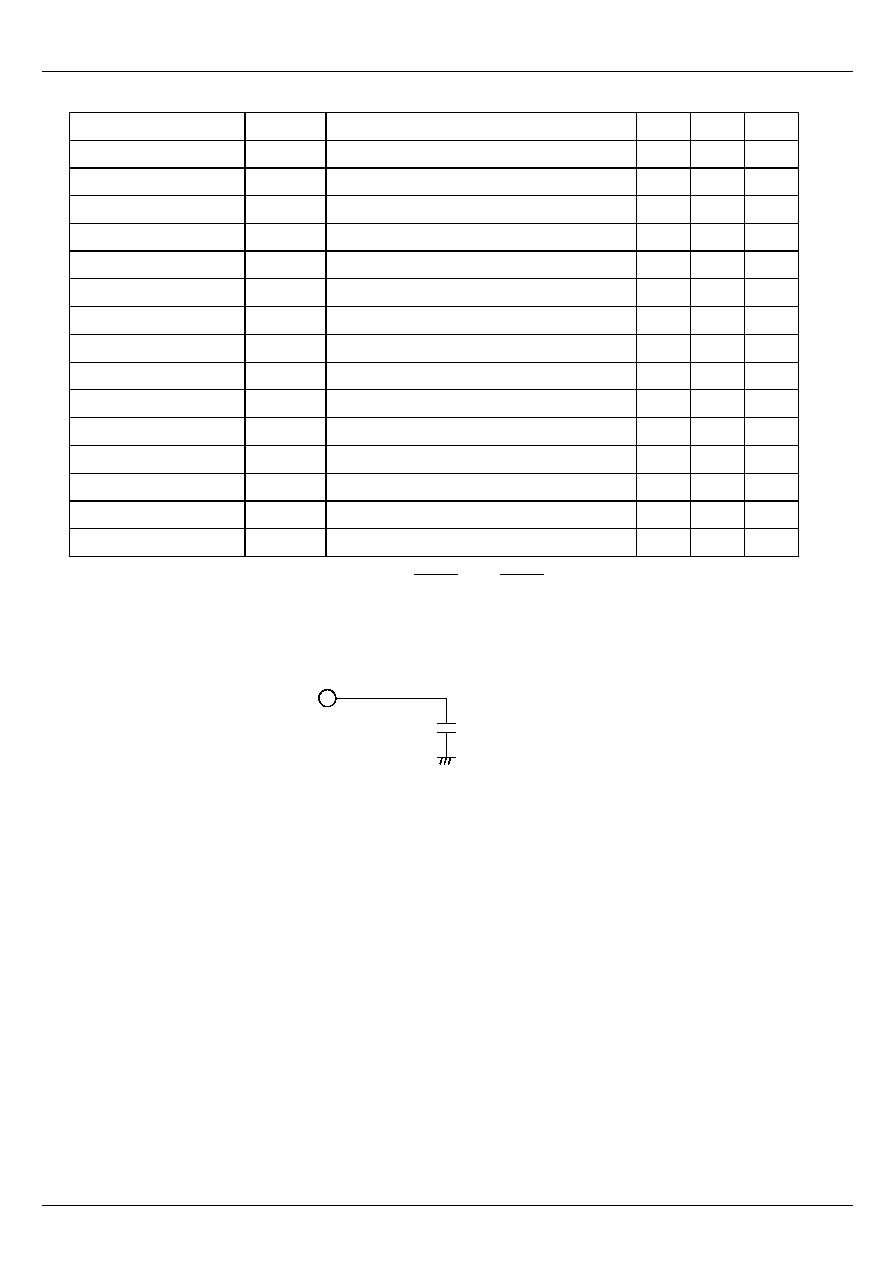
Item Symbol
Ratings
Unit
Notes
Power supply Logic circuit
Vdd
-0.3 to +7.0
V
1, 9
V
LCD
-0.3 to +25.0
V
1, 3, 9
V
EE
-20.0 to +0.3
V
1, 4, 9
Input voltage (1)
VT1
-0.3 to Vdd + 0.3
V
1, 2
Input voltage (2)
VH
+0.3 to V
LCD
V
1, 5, 9
Input voltage (3)
VL
-0.3 to V
EE
V
1, 6, 9
Input voltage (4)
VM
0.3 to + 5.0
V
1, 8, 9
Operating temperature
Topr
-30 to +75
�
C
Storage temperature
Tstg
-55 to +110
�
C
Notes: 1. The reference point is GND (0 V)
2. Applicable to DIO1, DISPOFF , SHL, M, MWS0~4, RESET MODE0, MODE1, CL, M /S, AMP, CCL,
DIO2
3. Applicable to V
LCDL
, V
LCDR
pins
4. Applicable to V
EEL
, V
EER
pins
5. Applicable to V
HL
, V
HR
pins
6. Applicable to V
LL
, V
LR
pins
7. Applicable to V
ML
, V
MR
pins
8. If the LSI is used beyond the above maximum ratings, it may be permanently damaged. It should always be
used within its specified operating range for normal operation to prevent malfunctions or degraded reliability.
9. Observe the sequence of activation and inactivation for the following power supplies and signals. And this
sequence applies to use built-in switching circuit. If the sequence is not observed, it may cause LSI
malfunction, permanent damage or adverse effect.
Sitronix ST8600
Ver 0.2
10/18
2001/Feb/28
Figure 14 Turn on and Turn off timing
Input signal,
clock, data
VM
V
LCD
, VH
Vdd
Signal undefined
period
initilization period
(larger than one frame)
(0ms: minimun specification)
0ms
0ms
0ms
0ms
0ms
0ms
2.5V
2.5V
DISPOFF
0ms
V
EE,
VL
8.1 Turning on the power
1) Turn on the power in the order of GND-Vdd,
GND-V
LCD
(VH), and VM. VM-GND is generated
automatically. In this case, input GND to the
DISPOFF pin.
2) The LCD forcibly outputs the VM level by the
DISPOFF function.
3) Even if an input signal is disturbed immediately
after Vdd is applied, the DISPOFF function has
priority.
4) Input the specific signal to initialize the registers
in the driver. The initialization period must be at
least one frame.
5) The preparation for the normal display is
completed. Apply the Vdd level to the DISP
pin to cancel the DISPOFF function. At this time,
the level of pins V
EE
(VL), V
LCD
(VH) and VM
must rise to the specific potential.
8.2 Turning off the power
The procedure is basically the reverse of that used to
turn on the power.
1) Ground
the DISPOFF pin.
2) At first shut off the LCD power supply
GND-V
LCD
(VH), at same time GND-V
EE
(VL) get
to VM. Next shut off the VM.
3) Ground Vdd, and an input signal.
4) At this time, the level of pins V
EE
(VL), V
LCD
(VH)
and VM must fall to 0 V. Since the DISPOFF
function stops when Vdd falls to 0 V, the LCD
may output a level other than VM. Therefore, a
display failure may occur when the power is
turned off or on.
Sitronix ST8600
Ver 0.2
11/18
2001/Feb/28
9
9
E
E
l
l
e
e
c
c
t
t
r
r
i
i
c
c
a
a
l
l
C
C
h
h
a
a
r
r
a
a
c
c
t
t
e
e
r
r
i
i
s
s
t
t
i
i
c
c
s
s
9.1 DC Characteristics 1 (Vdd = 2.5 to 5.5 V, GND =0V, V
LCD
-V
EE
=15 to 43V, Ta = -30 to +75 �C)
Item. Symbol
Applicable
Pin Min.
Typ.
Max.
Unit
Conditions
Notes
Input high-level
voltage
VIH 0.7Vdd
-
Vdd
V
Input low level
voltage
VIL
DISPOFF , M /S,
SHL, MWS0~4,
RESET , CL, MODE0,
MODE1, DOC , AMP,
CCL, DIO2 , DIO1, M
0 -
0.3Vdd
V
Output high- level
voltage
V
OH
Vcc-0.4
-
-
V
IOH = -0.4 mA
Output low-level
voltage
V
OL
M, DOC , DIO1, DIO2
-
-
0.4
V
IOL = 0.4 mA
Vi-Yj ON
resistance
RON
X1 to X240 and V pin
-
0.7
2 .0
K ION = 150 uA
Input leakage
current (1)
IIL1
DISPOFF , M /S,
SHL, MWS0~4,
RESET , CL, MODE0,
MODE1, DOC , AMP,
CCL, DIO2 , DIO1, M
-5.0 - 5.0
uA
V
IN
= Vdd-GND
Input leakage
current (2)
IIL2
VH, VL, VM, C1,C2
-25
-
25
uA
Current
consumption (1)
I
CC1
Vdd
-
10 40 uA
Vdd=3.3V
VLCD-VEE=40V,
f
CL2
=19.2kHz
f
M
= 1.5kHz
2
Current
consumption (2)
I
CC2
Vdd
-
20 50 uA
Vdd=5.0V
VLCD-VEE=40V,
f
CL2
=19.2kHz
f
M
= 1.5kHz
Current
consumption (3)
I
LCD
Vdd
-
25 50 uA
Vdd=3.3V
VLCD-VEE=40V,
f
CL2
=19.2kHz
f
M
= 1.5kHz
Sitronix ST8600
Ver 0.2
12/18
2001/Feb/28
Notes: 1. This is resistance value between the X and Y pins (either of VH, VL or VM) when a load current is applied to one
of X1 to X240 pins. These values are under the conditions of VLCD= VH = 21.75V, VEE = VL = -18.5V, VM = 1.75V,
GND = 0V, Use VH, VL and VM in the range of VLCD � VM>= VH � VM = 21.5 to 7.5V, VEE � VM <=VL-VM =
-21.5V to �7.5V with the relation of VH > VM > VL.
2. The current applied between the input and output is excluded. When an input to a CMOS gate is at an
intermediate level, through current flows between the power supplies and the power supply current increase.
Therefore use VIH = Vdd and VIL = GND.
3. The voltage relationship of each signal is as follows:
Segment waveform
Common waveform
Common
voltage
Segment
voltage
Normal display period
Display-off
period
Normal display period
Display-off
period
V0(5.0V)
Vcc(3.3V)
VM(3.0V)
V1(1.0V)
GND(0.0V)
Vcc(3.3V)
VM(3.0V)
GND(0.0V)
VL(-17.0V)
VH(23.0V)
Figure 16 Signal Voltage
Sitronix ST8600
Ver 0.2
13/18
2001/Feb/28
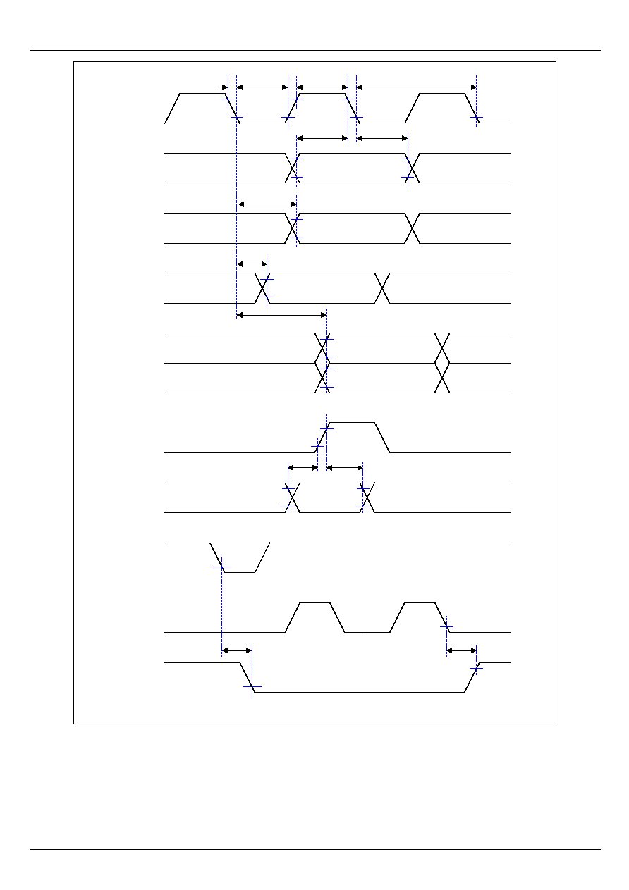
9.2
AC Characteristics 1 (Vdd=2.7 to 4.5V, V0-GND=3.5 to 5.5V, and Ta=-30 to +75
�
C)
Item Symbol
Applicable
Pins
Min
Max.
Unit
Clock cycle time
t
CYC
CL
400
-
ns
Clock high-level width (1)
t
CWH
CL
25
-
ns
Clock low-level width (1)
t
CWL
CL
370
-
ns
Clock rise time
tr
CL
-
30
ns
Clock fall time
tf
CL
-
30
ns
Data setup time
t
DS
DIO1, DIO2, CL
100
-
ns
Data hold time
t
DH
DIO1, DIO2, CL
10
-
ns
Data output delay time
t
DD
DIO1, DIO2, CL
-
200
ns
M output delay time
t
MD
M and CL
-
200
ns
M setup time
t
MS
M and CL
20
-
ns
M hold time
t
MH
M and CL
20
-
ns
Output delay time (1)
tpd1
M and X1 to X240
-
1.2
us
DOC delay time
t
DOC1
DISPOFF , DOC
- 300 ns
DOC delay time
t
DOC2
DIO1, DIO2, DOC
- 300 ns
Sitronix ST8600
Ver 0.2
14/18
2001/Feb/28
9.3
AC Characteristics 2 (Vdd = 4.5 to 5.5V, V0-GND=3.5 to 5.5V, and Ta= -30 to +75
�
C)
Item Symbol
Applicable
Pins
Min
Max.
Unit
Clock cycle time
t
CYC
CL2
25 - ns
Clock high-level width (1)
t
CWH2
CL2
10
-
ns
Clock low-level width (1)
t
CWL2
CL2
10
-
ns
Clock high-level width (2)
t
CWH1
CL1
25
-
ns
Clock setup time
t
SCL
CL1 and CL2
20
-
ns
Clock hold time
t
HCL
CL1 and CL2
50
-
ns
Clock rise time
tr
CL1 and CL2
-
20
ns
Clock fall time
tf
CL1 and CL2
-
20
ns
Data setup time
t
DS
D0 to D7 and CL2
6
-
ns
Data hold time
t
DH
D0 to D7 and CL2
6
-
ns
M setup time
t
MS
M and CL1
20
-
ns
M hold time
t
MH
M and CL1
20
-
ns
Output delay time (1)
tpd1
CL1 and Y1 to Y240
-
500
ns
CC setup time
t
CCS
CC3 to CC4, and CL1
20
-
ns
CC hold time
t
CCH
CC3 to CC4, and CL2
20
-
ns
Note: 1. The load must be less than 10 pF between the EIO1 and EIO2 connections of the ST8600
2. For output delay time 1 , connect the load circuit as shown in figure 17.
Test point
10pF
Figure 17 Load Circuit for Output Delay Time 1
Sitronix ST8600
Ver 0.2
15/18
2001/Feb/28
M
DIO1
DIO2
CL
0.3V
dd
0.3V
dd
t
DOC1
DIO1
DIO2
X(n)
CL
M
DISPOFF
DIO1
DIO2
(during input)
DOC
0.3V
cd
0.7V
dd
0.3V
dd
t
DOC2
0.7V
dd
0.3V
dd
0.7V
dd
t
MS
t
MH
0.7V
dd
0.3V
dd
0.7V
dd
0.3V
dd
0.7V
dd
0.3V
dd
V
OH
V
OL
V
OH
V
OL
0.7V
dd
0.3V
dd
0.7V
dd
0.3Vdd
t
CWL
t
f
t
CWH
t
f
t
CYC
t
DH
t
DS
t
pd1
t
MD
t
DD
Sitronix ST8600
Ver 0.2
16/18
2001/Feb/28
1
1
0
0
P
P
a
a
d
d
D
D
i
i
a
a
g
g
r
r
a
a
m
m
chip size = 13390 x 1710 um
substrate connect to VLL,VLR
unit: um
PAD No. PAD NAME
X
Y
PAD No. PAD NAME
X
Y
PAD No. PAD NAME
X
Y
1
DIO2
-5575
-724.6 113
X197
4071.4
755 225
X85
-1864.6
755
2
DUMMY_PAD -5267.5
-724.6 114
X196
4018.4
755 226
X84
-1917.6
755
3
DUMMY_PAD -5032.8
-724.6 115
X195
3965.4
755 227
X83
-1970.6
755
4
M
-4704.7
-724.6 116
X194
3912.4
755 228
X82
-2023.6
755
5
DUMMY_PAD -4397.2
-724.6 117
X193
3859.4
755 229
X81
-2076.6
755
6
RESET
-4115
-724.6 118
X192
3806.4
755 230
X80
-2129.6
755
7
DUMMY_PAD -3810.9
-724.6 119
X191
3753.4
755 231
X79
-2182.6
755
8
MWS4
-3538.2
-724.6 120
X190
3700.4
755 232
X78
-2235.6
755
9
MWS3
-3302.2
-724.6 121
X189
3647.4
755 233
X77
-2288.6
755
10
DUMMY_PAD -3021.3
-724.6 122
X188
3594.4
755 234
X76
-2341.6
755
11
DUMMY_PAD -2781.2
-724.6 123
X187
3541.4
755 235
X75
-2394.6
755
12
MWS2
-2505.6
-724.6 124
X186
3488.4
755 236
X74
-2447.6
755
13
MWS1
-2269.6
-724.6 125
X185
3435.4
755 237
X73
-2500.6
755
14
DUMMY_PAD -1994.7
-724.6 126
X184
3382.4
755 238
X72
-2553.6
755
15
MWS0
-1690.2
-724.6 127
X183
3329.4
755 239
X71
-2606.6
755
16
DUMMY_PAD -1428.7
-724.6 128
X182
3276.4
755 240
X70
-2659.6
755
17
VCC
-1325.6
-722.9 129
X181
3223.4
755 241
X69
-2712.6
755
18
VCC
-1250.6
-722.9 130
X180
3170.4
755 242
X68
-2765.6
755
19
VCC
-1175.6
-722.9 131
X179
3117.4
755 243
X67
-2818.6
755
20
VCC
-1100.6
-722.9 132
X178
3064.4
755 244
X66
-2871.6
755
21
VCC
-1025.6
-722.9 133
X177
3011.4
755 245
X65
-2924.6
755
22
VCC
-950.6
-722.9 134
X176
2958.4
755 246
X64
-2977.6
755
23
MODE1
-667.7
-724.6 135
X175
2905.4
755 247
X63
-3030.6
755
24
DUMMY_PAD
-407.8
-724.6 136
X174
2852.4
755 248
X62
-3083.6
755
25
DUMMY_PAD
-86.8
-724.6 137
X173
2799.4
755 249
X61
-3136.6
755
26
DUMMY_PAD
161.4
-724.6 138
X172
2746.4
755 250
X60
-3189.6
755
27
MODE0
455.3
-724.6 139
X171
2693.4
755 251
X59
-3242.6
755
28
DUMMY_PAD
714.5
-724.6 140
X170
2640.4
755 252
X58
-3295.6
755
29
DOCB
943.7
-730.3 141
X169
2587.4
755 253
X57
-3348.6
755
30
DUMMY_PAD
1180.3
-724.6 142
X168
2534.4
755 254
X56
-3401.6
755
31
DISPB
1479
-724.6 143
X167
2481.4
755 255
X55
-3454.6
755
32
DUMMY_PAD
1740.2
-724.6 144
X166
2428.4
755 256
X54
-3507.6
755
33
AMP
2010.3
-724.6 145
X165
2375.4
755 257
X53
-3560.6
755
34
DUMMY_PAD
2200.2
-724.6 146
X164
2322.4
755 258
X52
-3613.6
755
35
SHL
2521.4
-724.6 147
X163
2269.4
755 259
X51
-3666.6
755
36
DUMMY_PAD
2788.7
-724.6 148
X162
2216.4
755 260
X50
-3719.6
755
37
DUMMY_PAD
3108.8
-724.6 149
X161
2163.4
755 261
X49
-3772.6
755
38
DUMMY_PAD
3429.6
-724.6 150
X160
2110.4
755 262
X48
-3825.6
755
39
GND
3725.2
-723.1 151
X159
2057.4
755 263
X47
-3878.6
755
40
GND
3800.2
-723.1 152
X158
2004.4
755 264
X46
-3931.6
755
41
GND
3875.2
-723.1 153
X157
1951.4
755 265
X45
-3984.6
755
42
GND
3950.2
-723.1 154
X156
1898.4
755 266
X44
-4037.6
755
43
GND
4025.2
-723.1 155
X155
1845.4
755 267
X43
-4090.6
755
44
GND
4100.2
-723.1 156
X154
1792.4
755 268
X42
-4143.6
755
45
GND
4175.2
-723.1 157
X153
1739.4
755 269
X41
-4196.6
755
46
GND
4250.2
-723.1 158
X152
1686.4
755 270
X40
-4249.6
755
47
CL
4532.7
-724.6 159
X151
1633.4
755 271
X39
-4302.6
755
ST8600
X
1 X2 X3
X
2
4
0
X
2
3
9
X
2
3
8
D
U
M
M
Y
_
P
A
D
DUMMY_PAD
DUMMY_PAD
D
U
M
M
Y
_
P
A
D
D
U
M
M
Y
_
P
A
D
D
U
M
M
Y
_
P
A
D
D
U
M
M
Y
_
P
A
D
D
U
M
M
Y
_
P
A
D
D
U
M
M
Y
_
P
A
D
D
U
M
M
Y
_
P
A
D
D
U
M
M
Y
_
P
A
D
D
U
M
M
Y
_
P
A
D
D
U
M
M
Y
_
P
A
D
D
U
M
M
Y
_
P
A
D
D
U
M
M
Y
_
P
A
D
D
U
M
M
Y
_
P
A
D
D
U
M
M
Y
_
P
A
D
D
U
M
M
Y
_
P
A
D
D
U
M
M
Y
_
P
A
D
D
U
M
M
Y
_
P
A
D
D
U
M
M
Y
_
P
A
D
D
U
M
M
Y
_
P
A
D
D
U
M
M
Y
_
P
A
D
D
U
M
M
Y
_
P
A
D
D
U
M
M
Y
_
P
A
D
D
U
M
M
Y
_
P
A
D
D
U
M
M
Y
_
P
A
D
D
U
M
M
Y
_
P
A
D
D
U
M
M
Y
_
P
A
D
VHR
VHR
VHR
VMR
VMR
VMR
VLR
VLR
VLR
D
U
M
M
Y
_
P
A
D
VHL
VHL
VHL
VML
VML
VML
VML
VLL
VLL
VLL
VEO
VLL
VEO
VEO
VEO
Sitronix ST8600
Ver 0.2
17/18
2001/Feb/28
PAD No. PAD NAME
X
Y
PAD No. PAD NAME
X
Y
PAD No. PAD NAME
X
Y
48
DUMMY_PAD
4792.2
-724.6
160
X150
1580.4
755
272
X38
-4355.6
755
49
DUMMY_PAD
4904.6
-724.6
161
X149
1527.4
755
273
X37
-4408.6
755
50
CCL
5164.5
-724.6
162
X148
1474.4
755
274
X36
-4461.6
755
51
DUMMY_PAD
5467.7
-724.6
163
X147
1421.4
755
275
X35
-4514.6
755
52
MS
5666.5
-724.6
164
X146
1368.4
755
276
X34
-4567.6
755
53
DUMMY_PAD
5968.7
-724.6
165
X145
1315.4
755
277
X33
-4620.6
755
54
DIO1
6276.2
-724.6
166
X144
1262.4
755
278
X32
-4673.6
755
55
DUMMY_PAD
6545
-724.6
167
X143
1209.4
755
279
X31
-4726.6
755
56
DUMMY_PAD
6545
-511.9
168
X142
1156.4
755
280
X30
-4779.6
755
57
DUMMY_PAD
6545
-213.9
169
X141
1103.4
755
281
X29
-4832.6
755
58
VLR
6580.9
49.8
170
X140
1050.4
755
282
X28
-4885.6
755
59
VLR
6580.9
102.8
171
X139
997.4
755
283
X27
-4938.6
755
60
VLR
6580.9
155.8
172
X138
944.4
755
284
X26
-4991.6
755
61
VLR
6580.9
208.8
173
X137
891.4
755
285
X25
-5044.6
755
62
VMR
6580.9
261.8
174
X136
838.4
755
286
X24
-5097.6
755
63
VMR
6580.9
314.8
175
X135
785.4
755
287
X23
-5150.6
755
64
VMR
6580.9
367.8
176
X134
732.4
755
288
X22
-5203.6
755
65
VMR
6580.9
420.8
177
X133
679.4
755
289
X21
-5256.6
755
66
VHR
6580.9
473.8
178
X132
626.4
755
290
X20
-5309.6
755
67
VHR
6580.9
526.8
179
X131
573.4
755
291
X19
-5362.6
755
68
VHR
6580.9
579.8
180
X130
520.4
755
292
X18
-5415.6
755
69
DUMMY_PAD
6531.1
755
181
X129
467.4
755
293
X17
-5468.6
755
70
X240
6350.4
755
182
X128
414.4
755
294
X16
-5521.6
755
71
X239
6297.4
755
183
X127
361.4
755
295
X15
-5574.6
755
72
X238
6244.4
755
184
X126
308.4
755
296
X14
-5627.6
755
73
X237
6191.4
755
185
X125
255.4
755
297
X13
-5680.6
755
74
X236
6138.4
755
186
X124
202.4
755
298
X12
-5733.6
755
75
X235
6085.4
755
187
X123
149.4
755
299
X11
-5786.6
755
76
X234
6032.4
755
188
X122
96.4
755
300
X10
-5839.6
755
77
X233
5979.4
755
189
X121
43.4
755
301
X9
-5892.6
755
78
X232
5926.4
755
190
X120
-9.6
755
302
X8
-5945.6
755
79
X231
5873.4
755
191
X119
-62.6
755
303
X7
-5998.6
755
80
X230
5820.4
755
192
X118
-115.6
755
304
X6
-6051.6
755
81
X229
5767.4
755
193
X117
-168.6
755
305
X5
-6104.6
755
82
X228
5714.4
755
194
X116
-221.6
755
306
X4
-6157.6
755
83
X227
5661.4
755
195
X115
-274.6
755
307
X3
-6210.6
755
84
X226
5608.4
755
196
X114
-327.6
755
308
X2
-6263.6
755
85
X225
5555.4
755
197
X113
-380.6
755
309
X1
-6316.6
755
86
X224
5502.4
755
198
X112
-433.6
755
310
DUMMY_PAD
-6433.5
742
87
X223
5449.4
755
199
X111
-486.6
755
311
VHL
-6595
675.4
88
X222
5396.4
755
200
X110
-539.6
755
312
VHL
-6595
622.4
89
X221
5343.4
755
201
X109
-592.6
755
313
VHL
-6595
569.4
90
X220
5290.4
755
202
X108
-645.6
755
314
VML
-6595
516.4
91
X219
5237.4
755
203
X107
-698.6
755
315
VML
-6595
463.4
92
X218
5184.4
755
204
X106
-751.6
755
316
VML
-6595
410.4
93
X217
5131.4
755
205
X105
-804.6
755
317
VML
-6595
357.4
94
X216
5078.4
755
206
X104
-857.6
755
318
VLL
-6595
304.4
95
X215
5025.4
755
207
X103
-910.6
755
319
VLL
-6595
251.4
96
X214
4972.4
755
208
X102
-963.6
755
320
VLL
-6595
198.4
97
X213
4919.4
755
209
X101
-1016.6
755
321
VLL
-6595
145.4
98
X212
4866.4
755
210
X100
-1069.6
755
322
VEO
-6595
92.4
99
X211
4813.4
755
211
X99
-1122.6
755
323
VEO
-6595
39.4
100
X210
4760.4
755
212
X98
-1175.6
755
324
VEO
-6595
-13.6
101
X209
4707.4
755
213
X97
-1228.6
755
325
VEO
-6595
-66.6
102
X208
4654.4
755
214
X96
-1281.6
755
326
C1
-6595
-119.6
103
X207
4601.4
755
215
X95
-1334.6
755
327
C1
-6595
-172.6
104
X206
4548.4
755
216
X94
-1387.6
755
328
C1
-6595
-225.6
105
X205
4495.4
755
217
X93
-1440.6
755
329
C1
-6595
-278.6
106
X204
4442.4
755
218
X92
-1493.6
755
330
C2
-6595
-331.6
107
X203
4389.4
755
219
X91
-1546.6
755
331
C2
-6595
-384.6
108
X202
4336.4
755
220
X90
-1599.6
755
332
C2
-6595
-437.6
Sitronix ST8600
Ver 0.2
18/18
2001/Feb/28
PAD No. PAD NAME
X
Y
PAD No. PAD NAME
X
Y
PAD No. PAD NAME
X
Y
109
X201
4283.4
755
221
X89
-1652.6
755
333
C2
-6595
-490.6
110
X200
4230.4
755
222
X88
-1705.6
755
334
DUMMY_PAD
-6556
-755
111
X199
4177.4
755
223
X87
-1758.6
755
335
DUMMY_PAD
-6183.6
-724.6
112
X198
4124.4
755
224
X86
-1811.6
755
336
DUMMY_PAD
-5860.3
-724.6
Gold bump information (um):
X
Y
Pad No.
Pad name
Area
Output
38 66 309~70
X1~X240
2508
Output
58 60 29
DOC_B
3480
Input
58 60 15,13,12,9,8,6,17~22,39~46,27,23,31,33,35,47,50,52 MWS0~4,RESET,Vcc,GND,MODE0~1,DISPB,AMP,SHL,CL,CCL,MS 3480
I/O
58 60 54,1,4
DIO1,2,M
3480
Output
66 38 311~333,58~68
VEO,VHL,VHR,VML,VMR,VLL,VLR,C1,C2
2508
Dummy
85 62 2,3,5,7,10,11,14,16,24~26,28,30,32,34,36~38,48,49
DUMMY_PAD
5270
Bump pad height = 18um, strength = 18g