 | –≠–ª–µ–∫—Ç—Ä–æ–Ω–Ω—ã–π –∫–æ–º–ø–æ–Ω–µ–Ω—Ç: ST8616 | –°–∫–∞—á–∞—Ç—å:  PDF PDF  ZIP ZIP |

ST
Sitronix
ST8616
PRELIMINARY
168 Segment Driver for STN LCD with Low-Voltage Drive
Notice: This is not a final specification. Some parameters are subject to change
Ver 0.03
1/25
2001/Dec/13
1
1
F
F
e
e
a
a
t
t
u
u
r
r
e
e
s
s
168/160 output mode
LCD drive voltage: 2.6 to 5.5 V
168 LCD drive circuits
Operating voltage: 2.5 to 5.5 V
Shift clock speed
20 MHz max / 3 V
30 MHz max / 5 V
4/8 bits data bus
Display-off function
Automatic generation of the chip enable signal
Standby function
2
2
D
D
e
e
s
s
c
c
r
r
i
i
p
p
t
t
i
i
o
o
n
n
The ST8616 is a 168-channel segment driver that drives a
dot matrix LCD panel at low voltage. The ST8616 can
operate with a 5V LCD drive voltage and a 3V logic drive
voltage, and it can be used together with the common
driver ST8600 and ST8601. The ST8616, packaged in a
fine-pitch slim tape-carrier package (slim-TCP), makes it
possible to reduce the space round the LCD panel.
Sitronix ST8616
Ver 0.03
2/25
2001/Dec/13
3
3
P
P
i
i
n
n
a
a
s
s
s
s
i
i
g
g
n
n
m
m
e
e
n
n
t
t
(
(
T
T
C
C
P
P
)
)
SHL
D
1
D
0
D
3
D
2
D
5
D
4
D
7
D
6
CL2
CL1
M
GND1
V
1R
V
0R
V
MR
Top view
Y165
Y166
Y167
Y168
187
186
185
183
184
181
182
179
180
177
178
176
175
174
173
172
171
170
169
165
166
167
168
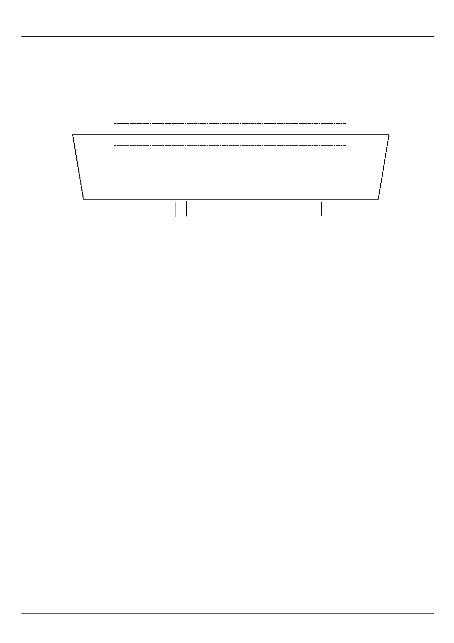
Figure 1 ST8616 TCP pin assignment
GND2
188
DISP
EIO
1
EIO
2
V
ML
V
0L
V
1L
194
193
192
V
DD
191
BS
189
MODE
190
Y1
Y2
Y3
Y4
1
2
3
4

Sitronix ST8616
Ver 0.03
3/25
2001/Dec/13
4
4
B
B
l
l
o
o
c
c
k
k
D
D
i
i
a
a
g
g
r
r
a
a
m
m
LCD Drive Circuit
Level Shifter
21 Bit Shift register
latch circuit (1)
(8 Bits)
latch circuit (1)
(8 Bits)
data shifter and
arithmetic circuit
CL2
8 bits
SHL
D0~D7
Y1~Y168
CL1
M
DISP
EIO1
EIO2
BS
VMR
V1R
V0R
VML
V0L
V1L
Latch circuit (2)
MODE
5
5
B
B
l
l
o
o
c
c
k
k
F
F
u
u
n
n
c
c
t
t
i
i
o
o
n
n
s
s
LCD Drive Circuit
The 168-bit LCD drive circuit selects three voltage levels
V
0
, V
1
and V
M
to drive the LCD panel. One of these three
levels is output to the corresponding Y pin, depending on
the data in latch circuit (2) and the DISP signal.
Data Shifter and Arithmetic Circuit
The data shifter shifts the destinations of data output when
necessary. The arithmetic circuit performs operations for
the data and AC signal M.

Sitronix ST8616
Ver 0.03
4/25
2001/Dec/13
Latch Circuit (2)
A 168-bit latch circuit (2) latches data which input from
latch circuit (1), and outputs the latched data to the level
shifter, at the falling edge of each clock 1 (CL1) pulse.
Latch Circuit (1)
The latch circuit (1) latches 4/8-bit parallel data which input
from D
0
to D
7
pins, and outputs the latched data to latch
circuit (2).
Shift Register
The 21-bit shift register generates and outputs data latch
signals for latch circuit (1) at the falling edge of each clock
2 (CL2) pulse.
Level Shifter
Converts logic signals to LCD drive signals.

Sitronix ST8616
Ver 0.03
5/25
2001/Dec/13
6
6
P
P
i
i
n
n
D
D
e
e
s
s
c
c
r
r
i
i
p
p
t
t
i
i
o
o
n
n
PIN NO.
SYMBOL
I/O
DESCRIPTION
1~168 Y1~Y168
O
Either level V
0
or V
1
is output according to the combination of the M signal and
display data when the DISP pin is set at V
DD
. See figure 4
193,170
194,169
192,171
V
0L
, V
0R
V
ML
, V
MR
V
1L
, V
1R
P
LCD drive-level voltage. See figure 3
191
172,188
V
DD
,
GND1, GND2
P
Logic power supply
175 CL1
I Display data latch signal. The LCD drive signal corresponding to the display data is
output at the falling edge of this signal.
176
CL2
I Display data latch signal. Display data is latched at the falling edge of this signal.
174
M
I Changes the LCD drive outputs to AC.
184~177 D
0
~D
7
I
When the display data is 1 (V
DD
level), the LCD drive output level is the selection
level and the liquid-crystal display is on, and when it is 0 (GND level), they are
non-selection level and off, respectively.
187 SHL
I
A control signal to switch the data output destination. See the section on Switching
the Data Output Destination.
186,173 EIO1 , EIO2 I/O
If SHL is at the GND level, EIO1 inputs the chip enable signal and EIO2
outputs the chip enable signal; and if it is at the V
DD
level, the opposite occurs.
Enable input: The chip enable-input pin of the first ST8616 must be fixed to the GND
level, and the other chip-enable input pins must be connected to the chip
enable-output pins of the previous ST8616.
Enable output: The chip enable-output pin must be connected to the chip
enable-input pin of the next ST8616.
185
DISP
I When DISP is GND level, it sets LCD drive outputs (Y1 to Y168) to the V
M
level.
189
BS
I
4/8 bit data selection. Connect to V
DD
when use 8-bit data mode, connect to ground
when use 4 bit data mode (capture data from D
0
~D
4
, D
4
~
7
connect to ground)
190
MODE
I
160/168 outputs mode selection. Connect to V
DD
when use 168 outputs mode,
connect to ground when use 160 outputs mode.
P: power pin
V
0
V
1
V
0
V
1
D
M
1
0
0
0
1
1
Figure 4 Selection of LCD Drive Output Level
Output level

Sitronix ST8616
Ver 0.03
6/25
2001/Dec/13
Switching the Data Output Destination
The order for the output of captured data is inverted crosswise according to the SHL signal. At this time, the input/output
pin of the enable signal can be switched. See figure 5-1 , figure 5-2.
D3
D2
D1
D0
D3
D2
D1
D0
D3
D2
D1
D0
D3
D2
D1
D0
D3
D2
D1
D0
D3
D2
D1
D0
D3
D2
D1
D0
D3
D2
D1
D0
Y168
Y167
Y165
Y166
Y164
Y163
Y161
Y162
Y8
Y7
Y5
Y6
Y4
Y3
Y1
Y2
Y8
Y7
Y5
Y6
Y4
Y3
Y1
Y2
SHL = GND , BS=GND , MODE=V
DD
Enable input : EIO1
Enable output : EIO2
Enable input : EIO2
Enable output : EIO1
Figure 5-1 Data Output Destination ( 168-output mode
)
first data
last data
Y168
Y167
Y165
Y166
Y164
Y163
Y161
Y162
last data
first data
D0
D1
D2
D3
D4
D5
D6
D7
D0
D1
D2
D3
D4
D5
D6
D7
Y8
Y7
Y5
Y6
Y4
Y3
Y1
Y2
SHL = GND , BS = V
DD
, MODE=V
DD
Enable input : EIO1
Enable output : EIO2
Y168
Y167
Y165
Y166
Y164
Y163
Y161
Y162
last data
first data
D7
D6
D5
D4
D3
D2
D1
D0
D7
D6
D5
D4
D3
D2
D1
D0
Y8
Y7
Y5
Y6
Y4
Y3
Y1
Y2
Enable input : EIO2
Enable output : EIO1
Y168
Y167
Y165
Y166
Y164
Y163
Y161
Y162
last data
first data
SHL = V
DD
, BS = GND , MODE=V
DD
SHL = V
DD
, BS=V
DD
, MODE=V
DD

Sitronix ST8616
Ver 0.03
7/25
2001/Dec/13
D3
D2
D1
D0
D3
D2
D1
D0
D3
D2
D1
D0
D3
D2
D1
D0
D3
D2
D1
D0
D3
D2
D1
D0
D3
D2
D1
D0
D3
D2
D1
D0
Y160
Y159
Y157
Y158
Y156
Y155
Y153
Y154
Y8
Y7
Y5
Y6
Y4
Y3
Y1
Y2
Y8
Y7
Y5
Y6
Y4
Y3
Y1
Y2
SHL=GND , BS=GND , MODE=GND
SHL = V
DD
, BS=GND , MODE=GND
Enable input : EIO1
Enable output : EIO2
Enable input : EIO2
Enable output : EIO1
Figure 5-2 Data Output Destination ( 160-output mode )
first data
last data
Y160
Y159
Y157
Y158
Y156
Y155
Y153
Y154
last data
first data
D0
D1
D2
D3
D4
D5
D6
D7
D0
D1
D2
D3
D4
D5
D6
D7
Y8
Y7
Y5
Y6
Y4
Y3
Y1
Y2
SHL=GND , BS = V
DD
, MODE=GND
Enable input : EIO1
Enable output : EIO2
Y160
Y159
Y157
Y158
Y156
Y155
Y153
Y154
last data
first data
D7
D6
D5
D4
D3
D2
D1
D0
D7
D6
D5
D4
D3
D2
D1
D0
Y8
Y7
Y5
Y6
Y4
Y3
Y1
Y2
SHL = V
DD
, BS = V
DD
, MODE=GND
Enable input : EIO2
Enable output : EIO1
Y160
Y159
Y157
Y158
Y156
Y155
Y153
Y154
last data
first data

Sitronix ST8616
Ver 0.03
8/25
2001/Dec/13
Operation Timing
4-bit data mode, BS=GND ,SHL=GND ,MODE=GND
During the data standby state when the data latch
operation enable signal ( EIO1 , when SHL=GND) is low,
the next data latch clock (CL2) cancels the standby state.
The 4-bit data is latch at the falling edge of CL2. When it
has latched 156 bits of data, it sets the EIO2 signal to
low. When it has latched 160 bits of data, it automatically
stops and enters the standby state, initiating the next
ST8616, provided its EIO2 pin is connected to the
EIO1 pin of the next ST8616.
Figure 6-1 shows the 4-bit data-latch timing
When SHL = GND, the EIO1 pin is a chip-enable input
and the EIO2 pin is a chip-enable output, data d1 is
output to Y1 and d160 is output to Y160. When SHL =
V
DD
; the EIO1 pin is a chip-enable output and the
EIO2 pin is a chip-enable input, d1 is output to Y160 and
d160 is output to Y1.
Line
CL2
D
0
D
3
CL1
EIO2
(1)
EIO2
(2)
Y1 to Y320
ST8616 (2) latch data
ST8616 (1) latch data
Figure 6-1 4 bit data Latch Timing (1 line, 320 dots)
1
2
38
39
40
41
78
79
80
d4
d8
d1
d5
d160
d157
d156
d153

Sitronix ST8616
Ver 0.03
9/25
2001/Dec/13
4-bit data mode, BS=GND ,SHL=GND ,MODE=V
DD
During the data standby state when the data latch
operation enable signal ( EIO1 , when SHL=GND) is low,
the next data latch clock (CL2) cancels the standby state.
The 4-bit data is latch at the falling edge of CL2. When it
has latched 164 bits of data, it sets the EIO2 signal to
low. When it has latched 168 bits of data, it automatically
stops and enters the standby state, initiating the next
ST8616, provided its EIO2 pin is connected to the
EIO1 pin of the next ST8616.
Figure 6-1 shows the 4-bit data-latch timing
When SHL = GND, the EIO1 pin is a chip-enable input
and the EIO2 pin is a chip-enable output, data d1 is
output to Y1 and d168 is output to Y168. When SHL =
V
DD
; the EIO1 pin is a chip-enable output and the
EIO2 pin is a chip-enable input, d1 is output to Y168 and
d168 is output to Y1.
Line
CL2
D
0
D
3
CL1
EIO2
(1)
EIO2
(2)
Y1 to Y336
ST8616 (2) latch data
ST8616 (1) latch data
Figure 6-2 4 bit data Latch Timing (1 line, 336 dots)
1
2
39
40
41
42
80
81
82
d4
d8
d1
d5
d168
d165
d164
d161

Sitronix ST8616
Ver 0.03
10/25
2001/Dec/13
8-bit data mode, BS=V
DD ,
SHL=GND ,MODE=GND
Figure 6-3 shows the 8-bit data-latch timing. All operations are the same as 4-bit data mode.
Line
CL2
D
0
D
7
CL1
EIO2
(1)
EIO2
(2)
Y1 to Y320
ST8616 (2) latch data
ST8616 (1) latch data
Figure 6-3 8 bit data Latch Timing (1 line, 320 dots)
1
2
18
19
20
21
38
39
40
d8
d16
d1
d9
d160
d153
d152
d145

Sitronix ST8616
Ver 0.03
11/25
2001/Dec/13
8-bit data mode, BS=V
DD ,
SHL=GND ,MODE=V
DD
Line
CL2
D
0
D
7
CL1
EIO2
(1)
EIO2
(2)
Y1 to Y336
ST8616 (2) latch data
ST8616 (1) latch data
Figure 6-4 8 bit data Latch Timing (1 line, 336 dots)
1
2
19
20
21
22
40
41
42
d8
d16
d1
d9
d168
d161
d160
d152

Sitronix ST8616
Ver 0.03
12/25
2001/Dec/13
7
7
A
A
p
p
p
p
l
l
i
i
c
c
a
a
t
t
i
i
o
o
n
n
c
c
i
i
r
r
c
c
u
u
i
i
t
t
COM1
COM2
COM3
COM162
SEG1
COM161
COM160
SEG2
SEG3
SEG320
SEG319
SEG318
LCD PANEL
320X162 DOT MATRIX
X1~X162
ST8601
X1~X160
X1~X160
ST8616
ST8616
EIO
2
EIO
1
EIO
1
V
DD
MODE0, MODE1
M/S, AMP
MWS0~4
RESET
GND
SHL
C1
C2
VEO
V
LL,R
V
HL,R
V
ML,R
DISPOFF
M
DOC
DIO
1
CL , CCL
CL1
CL2
DISP
M
D0~D3
GND, BS, MODE
D
4
~D
7
, SHL
VDD
V
0L,R
V
1L,R
V
ML,R
CL1
CL2
DISP
M
D0~D3
GND, BS, MODE
D
4
~D
7
, SHL
VDD
V
0L,R
V
1L,R
V
ML,R
V
DD
DISP
FLM
CL1
CL2
D
0
~D
3
Controller
VLCD
V0
VM
V1
Power Supply
Circuit

Sitronix ST8616
Ver 0.03
13/25
2001/Dec/13
8
8
A
A
b
b
s
s
o
o
l
l
u
u
t
t
e
e
M
M
a
a
x
x
i
i
m
m
u
u
m
m
R
R
a
a
t
t
i
i
n
n
g
g
s
s
Item Symbol
Ratings
Unit
Notes
Power supply Logic circuit
V
DD
-0.3 to +7.0
V
2 and 5
LCD drive circuit
V
0
-0.3 to +7.0
V
2 and 5
Input voltage (1)
V
T1
-0.3
to
V
DD
+ 0.3
V
2 and 3
Input voltage (2)
V
T2
-0.3
to
V
0
+ 0.3
V
2, 4, and 5
Operating temperature
T
OPR
-30
to
+75
∞
C
Storage temperature
T
STG
-55
to
+110
∞
C
Notes: 1. If the LSI is used beyond the above maximum
ratings, it may be permanently damaged. It
should always be used within its specified
operating range for normal operation to
prevent malfunctions or degraded reliability.
2. The reference point is GND (0 V)
3. Applies to the SHL, EIO1 , EIO2 ,
DISP , D
0
to D
7
, CL1, CL2, M, and BS
pins.
4. Applies to the V
ML
, V
MR
, V
1L
, and V
1R
pins.
5. As shown in figure 14, users should conform
to the following turn-on/off sequence for the
power and signals. Otherwise, the LSI will
malfunction or will be permanently damaged.
In addition, the LSI reliability will be affected.
Figure 14 Turn on and Turn off timing
Input signal
clock data
Signal undefined
period
initilization period
(at least one frame)
V
0
,V
M
,V
1
V
DD
2.7V
2.7V
V
0
V
M
V
1
DISP

Sitronix ST8616
Ver 0.03
14/25
2001/Dec/13
5.1 Turning on the power
1) Turn on the power in the order of GND - V
DD
,
GND-V
0
and V
M
/V
1
. Then, ground the DISP
pin.
2) The LCD forcibly outputs the V
M
level by the
display-off function.
3) The display-off function has priority even if an
input signal is disturbed immediately after V
DD
is
applied.
4) Input the specific signal to initialize the registers
in the driver. The initialization period must be at
least one frame.
5) After the preparation for the normal display is
completed. Apply the V
DD
level to the DISP
pin to cancel the display-off function. At this time,
the level of pins V
0
, V
M
, and V
1
must rise to the
specific potential.
5.2 Turning off the power
The procedure is basically the reverse of that used to
turn on the power.
1) Ground
the DISP pin.
2) Turn off the LCD power in the order of V
M
/V
1
and GND-V
0
.
3) Set
V
DD
and input signals to GND.
At this time, the level of pins V
0
, V
M
, and V
1
must be 0V. Since the display-off function stops
when V
DD
falls to 0V, the LCD may output a
level other than V
M
. Therefore, a display failure
may occur when the power is turned off or on.

Sitronix ST8616
Ver 0.03
15/25
2001/Dec/13
9
9
E
E
l
l
e
e
c
c
t
t
r
r
i
i
c
c
a
a
l
l
C
C
h
h
a
a
r
r
a
a
c
c
t
t
e
e
r
r
i
i
s
s
t
t
i
i
c
c
s
s
9.1 DC Characteristics 1 (V
DD
= 2.7 to 4.5 V, V
0
-GND =3.5 to 5.5 V, and Ta = -30 to +75 ∫C)
Item. Symbol Applicable
Pin Min.
Typ.
Max.
Unit
Conditions
Notes
Input high-level
voltage
V
IH
0.7V
DD
-
V
Input low level
voltage
V
IL
CL1, CL2, SHL, M,
EIO1 , EIO2 , DISP
D
0
to D
7
, MODE, and BS
0 -
0.3V
DD
V
Output high- level
voltage
V
OH
V
DD
-0.4 -
-
V I
OH
= -0.4 mA
Output low-level
voltage
V
OL
EIO1 and EIO2
- -
0.4
V
I
OL
= 0.4 mA
Y1 to Y168, V
0L
and V
0R
0.5
2
.0
k
Y1 to Y168, V
ML
and V
MR
- 0.7 3.0 k
Vi-Yj on resistance R
ON
Y1 to Y168, V1L and V1R
-
0.8
2.0
k
I
ON
= 200 uA
Input leakage
current (1)
I
IL1
CL1, CL2, SHL, MODE,
EIO1 , EIO2 DISP ,
D
0
~D
7
, M and BS
-5.0 - 5.0 uA
V
IN
=-GND
Input leakage
current (2)
I
IL2
V
ML
, V
MR
, V
1L
and V
1R
-25
-
25
uA V
IN
= V
0
-GND
Current
consumption (1)
I
DD
V
DD
-
200
uA
2
Current
consumption (2)
I
V0
V
0L
and V
0R
-
100
500
uA
Current
consumption (3)
I
ST
V
DD
-
100
uA
V
DD
=3.0V
V
0
=4.5V
f
CL2
=20MHz
f
CL1
= 33.3 kHz
f
M
= 2.78 kHz 2, 3

Sitronix ST8616
Ver 0.03
16/25
2001/Dec/13
9.2
DC Characteristics 2(V
DD
= 4.5 to 5.5 V, V
0
-GND = 2.6 to 5.5 V and Ta = -30 to +75 ∫C)
Item. Symbol
Applicable
Pin Min.
Typ.
Max.
Unit
Conditions
Notes
Input high-level
voltage
V
IH
0.7V
DD
- V
DD
V
Input low level
voltage
V
IL
CL1, CL2, SHL, M,
EIO1 , EIO2 , DISP
D0 to D7, MODE, and BS
0 -
0.3V
DD
V
Output high- level
voltage
V
OH
V
DD
-0.4 -
- V
I
OH
= -0.4 mA
Output low-level
voltage
V
OL
EIO1 and EIO2
- -
0.4
V
I
OL
= 0.4 mA
Y1 to Y168, V
0L
and V
0R
0.5
2.0
k
Y1 to Y168, V
ML
and V
MR
- 0.7 3.0 k
Vi-Yj on resistance R
ON
Y1 to Y168, V
1L
and V
1R
- 0.8 2.0
k
I
ON
= 200 uA
1
Input leakage
current (1)
I
IL1
CL1, CL2, SHL, M,
EIO1 , EIO2 , DISP
D
0
to D
7
, MODE, and BS
-5.0 - 5.0
uA
V
IN
= V
DD
-GND
Input leakage
current (2)
I
IL2
V
ML
, V
MR
, V
1L
and V
1R
-25
-
25
uA V
IN
= V
0
-GND
Current
consumption (1)
I
DD
V
DD
-
0.6
mA
Current
consumption (2)
I
V0
V
0L
and V
0R
-
0.3
1.0
mA
2
Current
consumption (3)
I
ST
V
DD
-
0.2
mA
V
DD
=5.0V
V
0
= 4.5V
f
CL2
=30MHz
f
CL1
= 50 kHz
f
M
= 4.2 kHz
2, 3
Notes: 1. The resistance is between the LCD drive output
pins(Y1~Y168) and the voltage supply pins for
LCD panel (V0, VM, V1), when load current is
applied to one of the LCD drive output pins;
defined under the following conditions:
V
0
- GND = 5.5V
V
M
= (V0+V1) / 2
V
1
= GND + 1
V
1
should be near the GND level, and the V
M
should be near the middle voltage between V
1
and
V
0
. V
1
should be within the range of
V = 0.25 V
0
,
which is the range within which R
ON
, the LCD
drive circuits output impedance, is stable. See
figure 15.
2. Input and output currents are excluded. When a
CMOS input is left floating, excess current flows
from the power supply through the input circuit. To
avoid this, V
IH
and V
IL
must be used at V
DD
and
GND, respectively.
3. Standby current.
4. The voltage of each signal is shown in figure 16.

Sitronix ST8616
Ver 0.03
17/25
2001/Dec/13
Segment waveform
Common waveform
Common
voltage
Segment
voltage
Normal display period
Display-off
period
Normal display period
Display-off
period
V
M
GND
V
M
GND
V
L
V
H
Figure 16 Signal Voltage
V
0
V
1

Sitronix ST8616
Ver 0.03
18/25
2001/Dec/13
9.3
AC Characteristics 1 (V
DD
=2.7V, V
0
-GND=3.5 to 5.5V, f
CL2
=15MHz, and Ta=-30 to +75
∞
C)
Item Symbol
Applicable
Pins
Min
Max.
Unit
Clock cycle time
t
CYC
CL2
55
-
ns
Clock high-level width (1)
t
CWH2
CL2
15
-
ns
Clock low-level width (1)
t
CWL2
CL2
15
-
ns
Clock high-level width (2)
t
CWH1
CL1
55
-
ns
Clock setup time
t
SCL
CL1 and CL2
80
-
ns
Clock hold time
t
HCL
CL1 and CL2
80
-
ns
Clock rise time
tr
CL1 and CL2
-
30
ns
Clock fall time
tf
CL1 and CL2
-
30
ns
Data setup time
t
DS
D
0
to D
7
and CL2
10
-
ns
Data hold time
t
DH
D
0
to D
7
and CL2
10
-
ns
M setup time
t
MS
M and CL1
20
-
ns
M hold time
t
MH
M and CL1
20
-
ns
Output delay time (1)
t
PD1
CL1 and Y1 to Y168
-
500
ns
Note: 1. The load must be less than 10 pF between the EIO1 and EIO2 connections of the ST8616

Sitronix ST8616
Ver 0.03
19/25
2001/Dec/13
9.4
AC Characteristics 2 (V
DD
=5.0V, V0-GND=2.7 to 5.5V, f
CL2
=30MHz, and Ta=-30 to +75
∞
C)
Item Symbol
Applicable
Pins
Min
Max.
Unit
Clock cycle time
t
CYC
CL2
27 - ns
Clock high-level width (1)
t
CWH2
CL2
9
-
ns
Clock low-level width (1)
t
CWL2
CL2
9
-
ns
Clock high-level width (2)
t
CWH1
CL1
27
-
ns
Clock setup time
t
SCL
CL1 and CL2
91
-
ns
Clock hold time
t
HCL
CL1 and CL2
80
-
ns
Clock rise time
tr
CL1 and CL2
-
20
ns
Clock fall time
tf
CL1 and CL2
-
20
ns
Data setup time
t
DS
D
0
to D
7
and CL2
9
-
ns
Data hold time
t
DH
D
0
to D
7
and CL2
9
-
ns
M setup time
t
MS
M and CL1
20
-
ns
M hold time
t
MH
M and CL1
20
-
ns
Output delay time 1
t
PD
1
CL1 and Y1 to Y168
-
500
ns
Note: 1. The load must be less than 10 pF between the EIO1 and EIO2 connections of the ST8616
2. For output delay time 1 , connect the load circuit as shown in figure 17.
Test point
10pF
Figure 17 Load Circuit for Output Delay Time 1

Sitronix ST8616
Ver 0.03
20/25
2001/Dec/13
Y(n)
CL1
M
CL2
CL1
D
0
to D
7
CL2
Figure 18 AC Characteristics (1)
tr
t
CWH2
tf
t
CWL2
t
CYC
0.7V
DD
0.3V
DD
0.7V
DD
0.3V
DD
t
DH
t
DS
t
CWH1
0.7V
DD
0.3V
DD
t
SCL
t
HCL
0.3V
DD
t
MH
t
MS
0.7V
DD
0.3V
DD
0.3V
DD
t
PD1
0.8V
0
0.2V
1

Sitronix ST8616
Ver 0.03
21/25
2001/Dec/13
1
1
0
0
P
P
a
a
d
d
D
D
i
i
a
a
g
g
r
r
a
a
m
m
1 2
4142
212
43
Substrate Connect to Ground
V
0
V
M
V
M
DUMMY
DUMMY
V
0
V
1
V
1
GND
GND
GND
V
DD
V
DD
V
DD
MODE
BS
SHL
EIO
1
DOFFB
DI
0
DI
1
DI
2
DI
3
DI
4
DI
5
DI
6
DI
7
CL2
CL1
M
EIO
2
GND
GND
GND
V
1
V
1
V
0
V
0
V
M
V
M
DUMMY
DUMMY
DUMMY
Y168
Y167
Y166
Y165
Y164
DUMMY
Y1
Y2 Y3
Y4
Y5
(0,0)
ST8616
Chip Size = 9670 um X 930 um
X
Y
Unit: um
PAD NO.
NAME
X
Y
PAD NO.
NAME
X
Y
1 DUMMY -4653.6
-219.85
27 DI
7
1410.4
-219.85
2 DUMMY -4532.3
-219.85
28 CL2 1710.4
-219.85
3 V
M
-4281.8
-219.85
29 CL1 2010.4
-219.85
4 V
M
-4195.6
-219.85
30 M 2310.4
-219.85
5 V
0
-3892
-219.85
31 EIO
2
2670.35
-219.85
6 V
0
-3805.8
-219.85
32 GND 2980.7
-219.85
7 V
1
-3521.8
-219.85
33 GND 3066.9
-219.85
8 V
1
-3435.6
-219.85
34 GND 3153.1
-219.85
9 GND -3216.6
-219.85
35 V
1
3451
-219.85
10 GND -3130.4
-219.85
36 V
1
3537.2
-219.85
11 GND -3044.2
-219.85
37 V
0
3821.2
-219.85
12 V
DD
-2839.35
-219.85
38 V
0
3907.4
-219.85
13 V
DD
-2753.15
-219.85
39 V
M
4211
-219.85
14 V
DD
-2666.95
-219.85
40 V
M
4297.2
-219.85
15 MODE
-2399.65
-219.85
41 DUMMY 4524.85
-219.85
16 BS
-2099.65
-219.85
42 DUMMY 4646.15
-219.85
17 SHL
-1799.65
-219.85
43 DUMMY 4767.5
337.4
18 EIO
1
-1499.65
-219.85
44 Y168 4677.3
337.4
19 DOFFB
-1199.65
-219.85
45 Y167 4621.3
337.4
20 DI
0
-899.65
-219.85
46 Y166 4565.3
337.4
21 DI
1
-414.35
-219.85
47 Y165 4509.3
337.4
22 DI
2
-114.35
-219.85
48 Y164 4453.3
337.4
23 DI
3
185.65
-219.85
49 Y163 4397.3
337.4
24 DI
4
499.65
-219.85
50 Y162 4341.3
337.4
25 DI
5
800.05
-219.85
51 Y161 4285.3
337.4
26 DI
6
1110.4
-219.85
52 Y160 4229.3
337.4

Sitronix ST8616
Ver 0.03
22/25
2001/Dec/13
PAD NO.
NAME
X
Y
PAD NO.
NAME
X
Y
53 Y159 4173.3
337.4
91 Y121 2045.3
337.4
54 Y158 4117.3
337.4
92 Y120 1989.3
337.4
55 Y157 4061.3
337.4
93 Y119 1933.3
337.4
56 Y156 4005.3
337.4
94 Y118 1877.3
337.4
57 Y155 3949.3
337.4
95 Y117 1821.3
337.4
58 Y154 3893.3
337.4
96 Y116 1765.3
337.4
59 Y153 3837.3
337.4
97 Y115 1709.3
337.4
60 Y152 3781.3
337.4
98 Y114 1653.3
337.4
61 Y151 3725.3
337.4
99 Y113 1597.3
337.4
62 Y150 3669.3
337.4
100 Y112 1541.3
337.4
63 Y149 3613.3
337.4
101 Y111 1485.3
337.4
64 Y148 3557.3
337.4
102 Y110 1429.3
337.4
65 Y147 3501.3
337.4
103 Y109 1373.3
337.4
66 Y146 3445.3
337.4
104 Y108 1317.3
337.4
67 Y145 3389.3
337.4
105 Y107 1261.3
337.4
68 Y144 3333.3
337.4
106 Y106 1205.3
337.4
69 Y143 3277.3
337.4
107 Y105 1149.3
337.4
70 Y142 3221.3
337.4
108 Y104 1093.3
337.4
71 Y141 3165.3
337.4
109 Y103 1037.3
337.4
72 Y140 3109.3
337.4
110 Y102 981.3
337.4
73 Y139 3053.3
337.4
111 Y101 925.3
337.4
74 Y138 2997.3
337.4
112 Y100 869.3
337.4
75 Y137 2941.3
337.4
113 Y99 813.3
337.4
76 Y136 2885.3
337.4
114 Y98 757.3
337.4
77 Y135 2829.3
337.4
115 Y97 701.3
337.4
78 Y134 2773.3
337.4
116 Y96 645.3
337.4
79 Y133 2717.3
337.4
117 Y95 589.3
337.4
80 Y132 2661.3
337.4
118 Y94 533.3
337.4
81 Y131 2605.3
337.4
119 Y93 477.3
337.4
82 Y130 2549.3
337.4
120 Y92 421.3
337.4
83 Y129 2493.3
337.4
121 Y91 365.3
337.4
84 Y128 2437.3
337.4
122 Y90 309.3
337.4
85 Y127 2381.3
337.4
123 Y89 253.3
337.4
86 Y126 2325.3
337.4
124 Y88 197.3
337.4
87 Y125 2269.3
337.4
125 Y87 141.3
337.4
88 Y124 2213.3
337.4
126 Y86
85.3
337.4
89 Y123 2157.3
337.4
127 Y85
30.3
337.4
90 Y122 2101.3
337.4
128 Y84
-26.7
337.4

Sitronix ST8616
Ver 0.03
23/25
2001/Dec/13
PAD NO.
NAME
X
Y
PAD NO.
NAME
X
Y
129 Y83
-82.7
337.4
167 Y45 -2210.7
337.4
130 Y82 -138.7
337.4
168 Y44 -2266.7
337.4
131 Y81 -194.7
337.4
169 Y43 -2322.7
337.4
132 Y80 -250.7
337.4
170 Y42 -2378.7
337.4
133 Y79 -306.7
337.4
171 Y41 -2434.7
337.4
134 Y78 -362.7
337.4
172 Y40 -2490.7
337.4
135 Y77 -418.7
337.4
173 Y39 -2546.7
337.4
136 Y76 -474.7
337.4
174 Y38 -2602.7
337.4
137 Y75 -530.7
337.4
175 Y37 -2658.7
337.4
138 Y74 -586.7
337.4
176 Y36 -2714.7
337.4
139 Y73 -642.7
337.4
177 Y35 -2770.7
337.4
140 Y72 -698.7
337.4
178 Y34 -2826.7
337.4
141 Y71 -754.7
337.4
179 Y33 -2882.7
337.4
142 Y70 -810.7
337.4
180 Y32 -2938.7
337.4
143 Y69 -866.7
337.4
181 Y31 -2994.7
337.4
144 Y68 -922.7
337.4
182 Y30 -3050.7
337.4
145 Y67 -978.7
337.4
183 Y29 -3106.7
337.4
146 Y66 -1034.7
337.4
184 Y28 -3162.7
337.4
147 Y65 -1090.7
337.4
185 Y27 -3218.7
337.4
148 Y64 -1146.7
337.4
186 Y26 -3274.7
337.4
149 Y63 -1202.7
337.4
187 Y25 -3330.7
337.4
150 Y62 -1258.7
337.4
188 Y24 -3386.7
337.4
151 Y61 -1314.7
337.4
189 Y23 -3442.7
337.4
152 Y60 -1370.7
337.4
190 Y22 -3498.7
337.4
153 Y59 -1426.7
337.4
191 Y21 -3554.7
337.4
154 Y58 -1482.7
337.4
192 Y20 -3610.7
337.4
155 Y57 -1538.7
337.4
193 Y19 -3666.7
337.4
156 Y56 -1594.7
337.4
194 Y18 -3722.7
337.4
157 Y55 -1650.7
337.4
195 Y17 -3778.7
337.4
158 Y54 -1706.7
337.4
196 Y16 -3834.7
337.4
159 Y53 -1762.7
337.4
197 Y15 -3890.7
337.4
160 Y52 -1818.7
337.4
198 Y14 -3946.7
337.4
161 Y51 -1874.7
337.4
199 Y13 -4002.7
337.4
162 Y50 -1930.7
337.4
200 Y12 -4058.7
337.4
163 Y49 -1986.7
337.4
201 Y11 -4114.7
337.4
164 Y48 -2042.7
337.4
202 Y10 -4170.7
337.4
165 Y47 -2098.7
337.4
203 Y9 -4226.7
337.4
166 Y46 -2154.7
337.4
204 Y8 -4282.7
337.4

Sitronix ST8616
Ver 0.03
24/25
2001/Dec/13
PAD NO
NAME
X
Y
PAD NO.
NAME
X
Y
205 Y7 -4338.7
337.4
209 Y3 -4562.7
337.4
206 Y6 -4394.7
337.4
210 Y2 -4618.7
337.4
207 Y5 -4450.7
337.4
211 Y1 -4674.7
337.4
208 Y4 -4506.7
337.4
212 DUMMY -4764.9 337.4
10.1 Gold Bump size (unit: um)
PAD
NO.
X Y
Area
(um
2
)
Output 44~211
38
95
3610
Input 3~40,
58
60
3480
Dummy 1,2,41,42,43,212
85
62
5270
Bump pad height = 18um, strength=18g

Sitronix ST8616
Ver 0.03
25/25
2001/Dec/13
Appendix
2001-Aug-24....................................... Page 16 - Correct condition of current consumption
Page 12 - Correct the name of ST8616 output pins
2001-Nov-16........................................Page 21~24 ≠ add PAD Diagram
2001-Dec-13 .......................................Page 21~24 ≠ Change chip center