 | –≠–ª–µ–∫—Ç—Ä–æ–Ω–Ω—ã–π –∫–æ–º–ø–æ–Ω–µ–Ω—Ç: AM114-609 | –°–∫–∞—á–∞—Ç—å:  PDF PDF  ZIP ZIP |
Skyworks Solutions, Inc. [781] 376-3000
∑ Fax [781] 376-3100 ∑ Email sales@skyworksinc.com ∑ www.skyworksinc.com
1
Specifications subject to change without notice. 12/02A
Single Band T/R Antenna
Switch Module 800≠1000 MHz
Features
LTCC Technology Integrating LPF/Coupler
GaAs PHEMT Switch Technology
SMD Package, 5.2 x 4 x 1.7 mm
Single Control with Low Current
Consumption
Applications
Transmit/Receive Antenna Switch for
Wireless System with Integrated LPF
and Coupler for Power Detection
AM114-609
Description
The AM114-609 is a high power antenna switch with an
LTCC low pass filter and LTCC coupler included for power
detection. The switches are PHEMT GaAs FETs that can
operate at 2.5 V with low DC current drain.
Preliminary
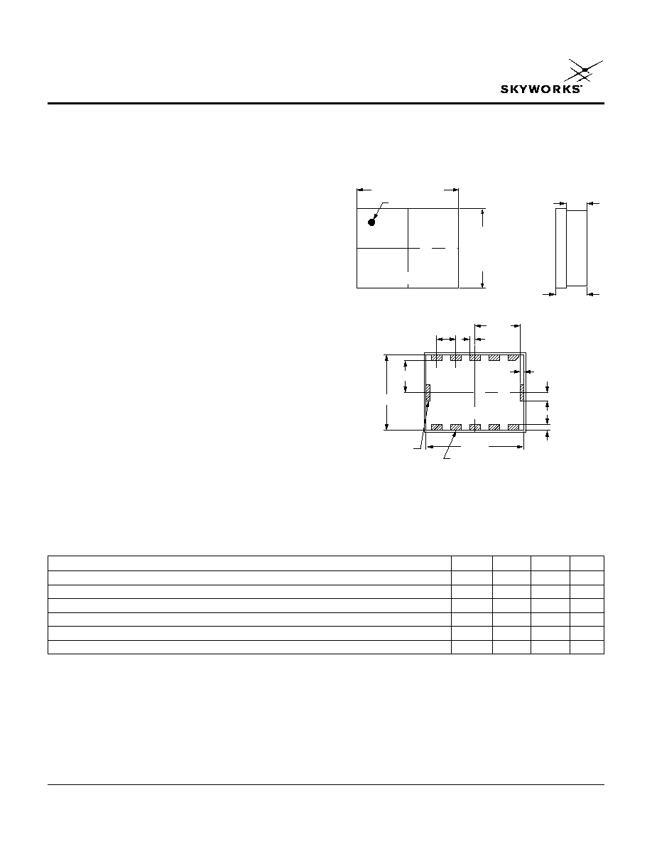
PIN 1 INDICATOR
5.40 MOLD CAP
DIMENSION ONLY
4.20
MOLD CAP
DIMENSION
ONLY
1.10 ± 0.05
1.66
TOP VIEW
BOTTOM VIEW
SIDE VIEW
Dimensions in mm. Tolerance ± 0.2 unless otherwise specified.
PIN 1
PIN 11
8X 1.00
4X 0.30
4X 2.40
10X 1.70
4.00
2X 0.20
4X 0.40
10X 0.30
METAL
PAD 2X
METAL PADS 10X
5.20
Outline Drawing
Parameter
Min.
Typ.
Max.
Unit
Frequency Range
851
941
MHz
Insertion Loss
0.6
0.8
dB
VSWR In-Band
1.5:1
RF Input Power
0
dBm
R
X
Current @ V
S
= 3 V
30
µA
Supply Voltage (V
S
)
2.7
3.0
5.0
V
Electrical Specifications @ 25∞C
Receive Path
Single Band T/R Antenna Switch Module 800≠1000 MHz
AM114-609
2
Skyworks Solutions, Inc. [781] 376-3000
∑ Fax [781] 376-3100 ∑ Email sales@skyworksinc.com ∑ www.skyworksinc.com
Specifications subject to change without notice. 12/02A
Parameter
Min.
Typ.
Max.
Unit
Frequency Range
806
928
MHz
Insertion Loss
0.8
1.0
dB
Isolation T
X
- R
X
in T
X
Mode (V
CTL
= 0 V)
25
dB
Inter-modulation 3rd/5th Order
-60
dBc
Inter-modulation 3rd/5th Order ≠ Under VSWR
-55
dBc
Input VSWR In-Band
1.5:1
Harmonic Rejection
2*F
O
15
dB
3*F
O
20
dB
Directivity
15
dB
Coupling Factor
19
20
21
dB
T
X
Current
150
µA
Supply Voltage (V
S
)
2.7
3.0
5.0
V
RF Input Power
3.0
dBm
Transmit Path
Characteristic
Value
Operating Temperature Range (T
OP
)
-30 to +85∞C
Storage Temperature Range (T
STG
)
-40 to +85∞C
Input Power (P
IN
)
38 dBm
Control Voltage Logic 0
-0.1 to 0.2 V
Supply Voltage (V
S
)
5 V
Nominal I/O Impedance
50
(T
X
, R
X
, Ant)
Absolute Maximum Ratings
Single Band T/R Antenna Switch Module 800≠1000 MHz
AM114-609
Skyworks Solutions, Inc. [781] 376-3000
∑ Fax [781] 376-3100 ∑ Email sales@skyworksinc.com ∑ www.skyworksinc.com
3
Specifications subject to change without notice. 12/02A
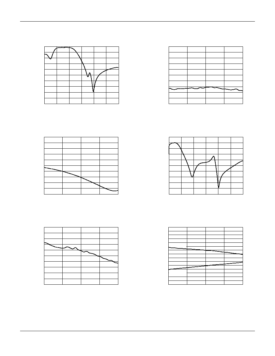
Frequency (GHz)
T
X
Insertion Loss vs. Frequency
Insertion Loss (dB)
-50
-45
-40
-35
-30
-25
-20
-15
-10
-5
0
0
0.5
1.0
1.5
2.0
2.5
3.0
Frequency (GHz)
T
X
Insertion Loss vs. Frequency
Insertion Loss (dB)
0.80
0.85
0.90
0.95
1.00
-1.0
-0.9
-0.8
-0.7
-0.6
-0.5
-0.4
-0.3
-0.2
-0.1
0
Frequency (GHz)
T
X
VSWR vs. Frequency
VSWR
1.0
1.1
1.2
1.3
1.4
1.5
1.6
1.7
1.8
1.9
2.0
0.80
0.85
0.90
0.95
1.00
Frequency (GHz)
R
X
Insertion Loss vs. Frequency
Insertion Loss (dB)
0.80
0.85
0.90
0.95
1.00
-1.0
-0.9
-0.8
-0.7
-0.6
-0.5
-0.4
-0.3
-0.2
-0.1
0
Frequency (GHz)
Coupling vs. Frequency
Coupling (dB)
0.80
0.85
0.90
0.95
1.00
-25
-24
-23
-22
-21
-20
-19
-18
-17
-16
-15
-14
-13
-12
-11
-10
Coupling
Directivity
Typical Performance Data
Frequency (GHz)
T
X
to R
X
Isolation vs. Frequency
Isolation (dB)
-50
-45
-40
-35
-30
-25
-20
-15
-10
-5
0
0
0.5
1.0
1.5
2.0
2.5
3.0
Single Band T/R Antenna Switch Module 800≠1000 MHz
AM114-609
4
Skyworks Solutions, Inc. [781] 376-3000
∑ Fax [781] 376-3100 ∑ Email sales@skyworksinc.com ∑ www.skyworksinc.com
Specifications subject to change without notice. 12/02A
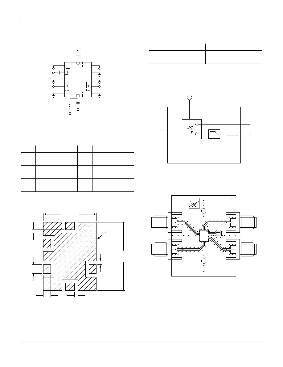
Blocking capacitors (47 pF) and inductor (82 nH) to be supplied externally.
Pin Out (Top View)
1
2
3
4
5
11
10
9
8
7
12
6
GND
GND
GND
GND
GND
GND
GND
CPLR
ANT
T
X
V
S
V
CTL
R
X
47 pF
47 pF
47 pF
Suggested Land Pattern
0.71
0.58
4.20
5.40
0.28
0.28
GND
0.28
Block Diagram
ANT
V
CTL
R
X
T
X
COUPLER
Pin
Description
Pin
Description
1
GND
7
GND
2
V
CTL
8
GND
3
GND
9
GND
4
R
X
10
Coupler
5
GND
11
GND
6
Ant
12
T
X
Pin Out Table
Dimensions are in mm.
PCB # SK40086, Material: FR4, Dielectric constant: 4.1.
The circuit board used in the final application should employ RF circuit design
techniques. RF signal lines should have 50
impedance. The package bottom
ground plane should be connected directly to PCB ground plane. A sufficient
number of via holes should be used to connect the top and bottom ground planes
of the PCB. The evaluation circuit board shown is available upon request.
Evaluation PCB
ANT
SK40086
REV -
CPLR
5.2 X 4 MM
IDEN T/R MODULE
ENM114-609
R
X
V
CTL
T
X
(GND)
Mode
V
CTL
T
X
0
R
X
Open Circuit
Truth Table
V
S
= 2.7 to 5 V supplied externally to T
X
port.