 | –≠–ª–µ–∫—Ç—Ä–æ–Ω–Ω—ã–π –∫–æ–º–ø–æ–Ω–µ–Ω—Ç: AP132-317 | –°–∫–∞—á–∞—Ç—å:  PDF PDF  ZIP ZIP |
Skyworks Solutions, Inc. [978] 241-7000
∑
Fax [978] 241-7906
∑
Email sales@skyworksinc.com
∑
www.skyworksinc.com
1
Specifications subject to change without notice. 2/02A
3 V InGaP DCS Power Amplifier
Features
Single Supply, 3.2 V Nominal
Operating Voltage
DCS1800 and PCS1900 Operation
Output Power Greater Than 33 dBm
High Power Added Efficiency of 50%
Ultra Small, Thermally Enhanced Micro
Leadframe Package
Low Current Standby Mode: < 10
µ
A
Integral Analog Power Control With
70 dB of Dynamic Range
GPRS Class 12 Capable
Designed to Work With AP131-317 as
a Dual-/Tri-Band Solution
-317
AP132-317
Description
The AP132-317 is a high performance IC power amplifier
designed for use as the final amplification stage in GSM or
GPRS mobile phones, and other digital wireless
applications in the 1700≠2000 MHz band. It features
3-cell battery operation, integrated analog power control
with over 70 dB of dynamic range, and exceptional power
added efficiency over the full battery voltage range. The
amplifier is manufactured on an advanced InGaP HBT
process, known industry-wide for its excellent reliability and
performance.The AP132-317 is designed to be stable over
a wide temperature range of -40 to +85∞C and over a
10:1 output VSWR load. Output matching is provided
externally to maximize performance, reduce costs, and allow
optimal matching for output power and efficiency over a
broader frequency range. A dual- and/or tri-band solution
can be obtained by combining the AP132-317 with
Alpha's AP131-317. The AP132-317 is packaged in a
thermally enhanced, ultra small micro leadframe package.
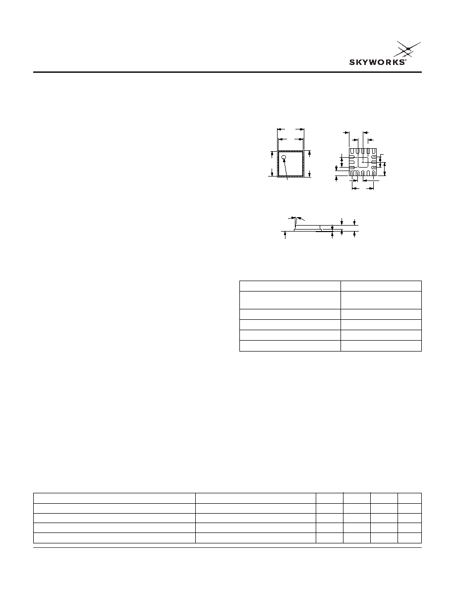
SEATING PLANE
12∞ MAX.
0.058
(1.47mm)
PIN
INDICATOR
0.058
(1.47 mm)
0.079
(2.00 mm)
0.025 (0.65 mm)
+ 0.004 (0.10 mm)
0.001 (0.025 mm)
+ 0.001 (0.025 mm)
0.039
(1.00 mm) MAX.
2
0.148
(3.75 mm)
BSC
0.157
(4.00 mm)
BSC
0.157
(4.00 mm) BSC
0.148
(3.75 mm)
BSC
1
16 1
2
0.062
(0.16 mm)
0.079
(2.00 mm)
0.031
(0.80 mm)
BSC
0.024
(0.60 mm)
REF.
0.124
(0.32 mm)
Preliminary
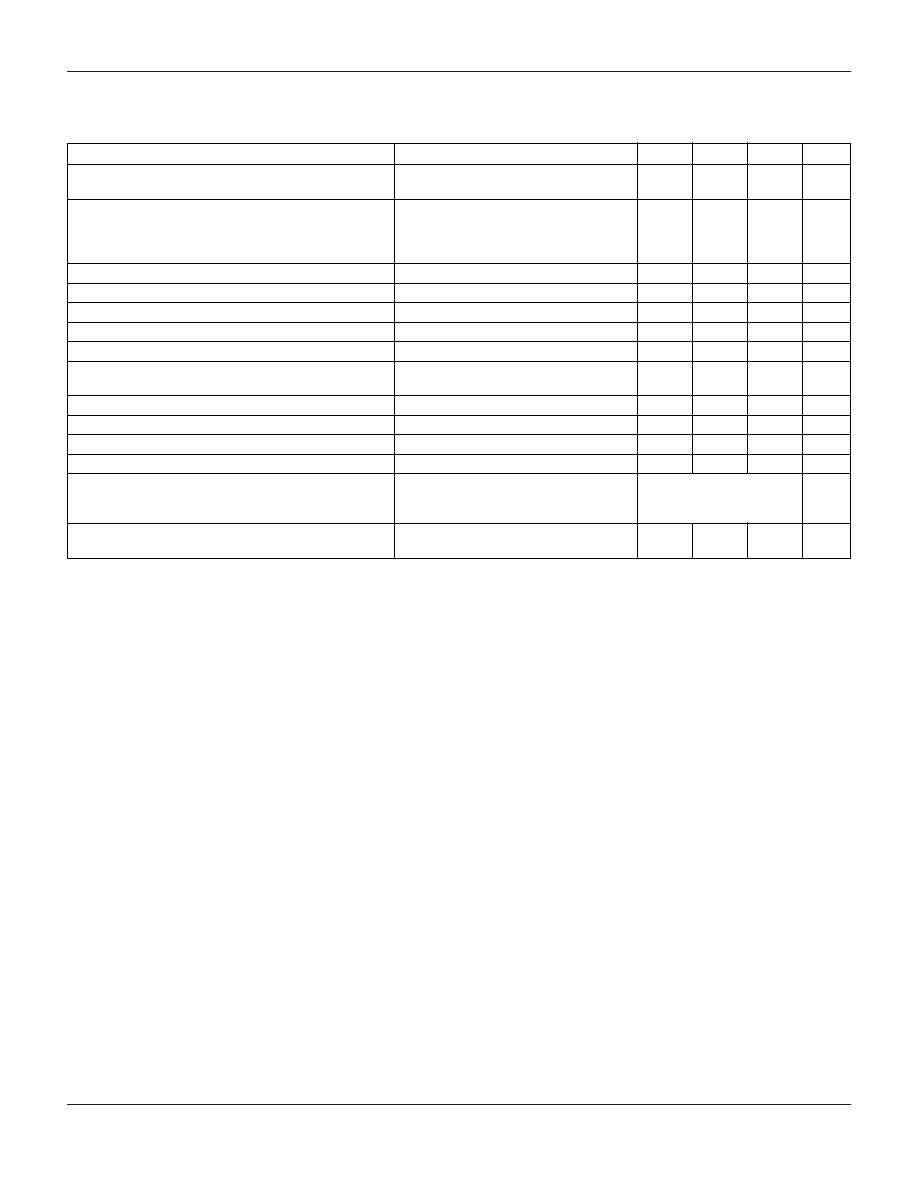
Characteristic
Value
Supply Voltage V
CC
, Standby Mode,
6 V Max.
V
APC
< 0.3 (No RF Input Power)
Power Control Voltage
4 V Max.
Input Power (CW)
15 dBm Max.
Operating Case Temperature
-40 to +85∞C
Storage Temperature
-45 to +120∞C
Absolute Maximum Ratings
Parameter
Condition
Min.
Typ.
Max.
Unit
Supply Voltage
2.8
3.2
4.2
V
Leakage Current
No Input RF Power
10
µ
A
Power Control Voltage
0.1
2.6
V
Power Control Current
V
APC1,2
= 2.6 V, V
CC
= 3.2 V, CW
5
mA
DC Specifications
3 V InGaP DCS Power Amplifier
AP132-317
2
Skyworks Solutions, Inc. [978] 241-7000
∑
Fax [978] 241-7906
∑
Email sales@skyworksinc.com
∑
www.skyworksinc.com
Specifications subject to change without notice. 2/02A
Parameter
Condition
Min.
Typ.
Max.
Unit
Frequency
DCS
1710
1785
MHz
PCS
1850
1910
MHz
Output Power
V
APC1,2
= 2.6 V, V
CC
= 3.2 V, CW
32.0
33.0
dBm
V
APC1,2
= 2.8 V, V
CC
= 3.5 V, CW
32.5
33.5
dBm
V
APC1,2
= 2.8 V, V
CC
= 2.7 V,
30.5
32.0
dBm
T = -20 to +85∞C, CW
Dynamic Range
V
APC
= 0.1 to 2.8 V
60
dB
Power Control Slope
V
APC
= 0.1 to 2.8 V
75
180
dB/V
APC
Power Added Efficiency
P
OUT
= P
OUT
Max.
42
50
%
Input Power
3
6
10
dBm
Input VSWR
P
OUT
= 0≠32.5 dBm
2:1
Forward Isolation
P
IN
= 6 dBm, V
APC
= 0.1 V
-40
dBm
P
IN
= 9 dBm, V
APC
= 0.1 V
-35
dBm
Second Harmonic
At P
OUT
Max., V
CC
= 3.2 V
-50
-45
dBc
Third Harmonic
At P
OUT
Max., V
CC
= 3.2 V
-60
-55
dBc
All Others Non-harmonic Spurious
-40
dBm
Noise in the R
X
Band
1805≠1880 MHz, 100 KHz BW
-76
dBm
Ruggedness
Output VSWR = 10:1 All Phase Angles,
No Module Damage
V
CC
= 4.2 V, P
IN
= 10 dBm, V
APC
= 2.6 V
or Permanent
Performance Degradation
Stability
Output VSWR = 10:1 All Phase Angles,
V
CC
= 4.2 V, P
IN
= 10 dBm, V
APC
= 2.6 V
-36
dBm
Electrical Specifications at 25∞C
Unless otherwise stated: pulsed operation @ 12.5% duty cycle, 50
system, V
CC
= 3.2 and T
A
= 25∞C.
3 V InGaP DCS Power Amplifier
AP132-317
Skyworks Solutions, Inc. [978] 241-7000
∑
Fax [978] 241-7906
∑
Email sales@skyworksinc.com
∑
www.skyworksinc.com
3
Specifications subject to change without notice. 2/02A
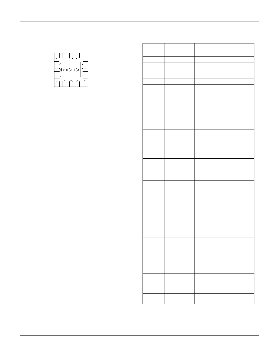
GND
N/C
2 F
0
GND
GND
RF In
2
4
3
12
10
11
RF Out
RF Out
RF Out
V
CC2
V
CC2
V
CC1
V
REF
GND
V
APC1
V
APC2
1
16
15
14
13
5
6
7
8
9
Pin Out
Pin Configuration
Pin
Symbol
Function
1
GND
Ground connection.
2
GND
Ground connection.
3
RF In
RF input to power amplifier. A
33 pF DC blocking capacitor is
required.
4
GND
Ground connection.
5
V
CC
Power supply input voltage.
1
µ
F and 33 pF RF bypassing
capacitors are required.
6
V
APC1
Power control input voltage for the
first two stages of the amplifier.
10 nF, 100 pF, and 10,000 pF RF
bypassing capacitors are required.
Can be connected to Pin 7 for
single power control operation.
7
V
APC2
Power control input voltage for
the third stage of the amplifier.
10 nF, 100 pF and 10,000 pF RF
bypassing capacitors are required.
Can be connected to Pin 6 for
single power control operation.
8
V
CC
Power supply input voltage.
10 nF, 1
µ
F and 100 pF RF
bypassing capacitors are required.
9
GND
Ground connection.
10
RF Out/V
CC3
1. RF output: Two shunt matching
capacitors, 4.5 pF high Q and
1.5 pF, and series 33 pF DC
blocking capacitors are required.
2. V
CC3
: 100 pF, 10 nF, and 1
µ
F
RF bypassing capacitors are
required.
11
RF Out/V
CC3
RF output and power supply input
voltage. See description for Pin 10.
12
RF Out/V
CC3
RF output and power supply input
voltage. See description for Pin 10.
13
2
Second harmonic termination.
This pin can be used to alter the
second harmonic output charac-
teristics, but for nominal GSM
operation, no matching elements
are required.
14
NC
No connect.
15
V
CC
Power supply input voltage.
1
µ
F, 100 pF, 10 nF, 5.6 pF and
10 pF interstage tuning and RF
bypassing capacitors are required.
16
V
CC
Power supply input voltage
connected to Pin 15.