
Data Sheet
Skyworks ≠ Preliminary
Doc. No. 101466C
Proprietary Information and Specifications Are Subject to Change
September 20, 2002
CX65001
160 ≠ 700 MHz Linear Power Amplifier Driver
Skyworks' CX65001 Microwave Monolithic Integrated Circuit (MMIC) power
amplifier driver offers a desirable combination of features that provide superb
performance and ease of use in a low-cost Surface-Mounted Technology (SMT)
package. The Gallium Arsenide (GaAs) Heterojunction Bipolar Transistor (HBT)
power amplifier driver was developed and optimized for extreme linear
performance in a variety of applications. It is ideal as a driver or output stage for
transceivers and repeaters for Trans-European Trunked Radio (TETRA), GSM400
and paging base stations, mobile radios, and many other applications.
Figure 1 shows a functional block diagram for the CX65001. The device package
and pinout are shown in Figure 2.
Driver Bias
Input Bias
Vcc1
8
5
2
3
6, 7
4
Y
Vcc2
VB
RFIN
RFOUT
DA
C1216
Figure 1. CX65001 Functional Block Diagram
Features
∑
5 V single supply operation
∑
Linear Pout of 24 dBm
∑
OIP3 of 45 dBm
∑
Internal bias circuits
∑
Surface mounted Small Outline Integrated Circuit
(SOIC) 8-pin package with downset ground paddle
Applications
∑
TETRA transceivers
∑
GSM400
∑
Wireless Local Loop (WLL) and Industrial,
Scientific, Medical (ISM) bands
∑
Repeaters
∑
Paging
∑
Mobile radios
∑
VHF/UHF TV broadcast
1
2
3
4
8
7
6
5
C1215
NC
VB
RFIN
Y
Vcc1
RFOUT
RFOUT
Vcc2
Figure 2. CX65001 Pinout ≠ 8-Pin SOIC Package
(Top View)

CX65001
Power Amplifier Driver
2
Skyworks ≠ Preliminary
101466C
Proprietary Information and Specifications Are Subject to Change
September 20, 2002
Electrical and Mechanical Specifications
The signal pin assignments and functions are described in
Table 1. The absolute maximum ratings of the CX65001 are
provided in Table 2. The recommended operating conditions are
specified in Table 3 and electrical specifications are provided in
Table 4.
Typical performance characteristics of the CX65001 are
illustrated in Figures 3 through 11.
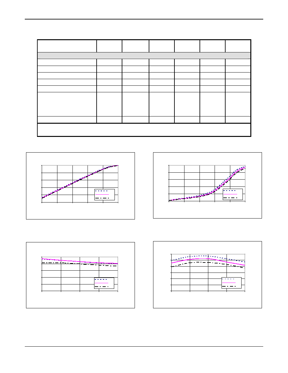
Table1. CX65001 Signal Descriptions
Pin #
Name
Description
1 NC
No
connection
2
VB
Input bias for driver amplifier
3 RFIN
RF
input
4
Y
Output of internal bias circuit
5 Vcc2
Supply
voltage
6 RFOUT
RF
output
7 RFOUT
RF
output
8 Vcc1
Supply
voltage
9 GND
Ground
Table 2. CX65001 Absolute Maximum Ratings
Parameter Symbol
Min
Typical
Max
Units
RF input power
P
IN
6 dBm
Supply voltage
Vcc
5.5
V
Supply current (l
D
+ l
BIAS
) I
CC
240
mA
Power
dissipation
1.3
W
Case operating temperature
T
C
≠40 +85 ∞C
Storage temperature
T
ST
≠55 125 ∞C
Junction temperature
T
J
150
∞C
Note: No damage to device if only one parameter is applied at a time with other parameters at nominal conditions.
Table 3. CX65001 Recommended Operating Conditions
Parameter Symbol
Min
Typical
Max
Units
Supply voltage
Vcc
5
V
Frequency range
F
160
700
MHz
Junction temperature
T
J
140
∞C
Maximum bias condition =
(Vcc
◊
I
D
) < (T
J
_
RECOMMENDED
≠ T
C
)/R
TH
,
J
-
C
Power Amplifier Driver
CX65001
101466C
Skyworks ≠ Preliminary
3
September 20, 2002
Proprietary Information and Specifications Are Subject to Change
Table 4. CX65001 Electrical Characteristics
(Vcc = 5 V, T
C
= 25 ∞C)
Parameter Symbol
Test
Conditions
Min Typical Max Units
OIP3 match, Frequency = 450 MHz (Note 1)
Supply current (l
D
+ l
BIAS
) I
CC
R
BIAS
= 270
120
130
mA
Small signal gain
G
P
IN
= ≠15 dBm
21
22
dB
Linear output power (Note 2)
P
OUT
P
IN
= +3 dBm
23
24
dBm
Power Added Efficiency
PAE
P
IN
= +3 dBm
35
42
%
Noise Figure (NF)
NF
4
5
dB
Output IP3
OIP3
Two CW tones
with 1 MHz
spacing
P
IN
= ≠16 dBm
per tone
42 45 dBm
Thermal resistance (junction ≠ case)
R
TH
,
J
-
C
91 ∞C/W
Note 1: Device matched for optimum OIP3 according to circuit shown in Figure 12.
Note 2: For reliable operation, do not violate the maximum input drive level specified in Table 2.
5
9
13
17
21
25
-15
-11
-7
-3
1
5
Pin (dBm)
P
out (dB
m
)
-40C
25C
85C
Figure 3. Typical Pout vs Pin @ 450 MHz Over Temperature
(Circuit Match for Optimum OIP3)
15
17
19
21
23
25
160
195
230
265
300
Freq (MHz)
S
m
all S
i
g
n
a
l Gain
(d
B)
-40C
25C
85C
Figure 5. Typical Small Signal Gain From 160 to 300 MHz Over
Temperature (Circuit Match for Optimum Gain)
0
10
20
30
40
50
-15
-11
-7
-3
1
5
Pin (dBm)
PAE (
%
)
-40C
25C
85C
Figure 4. Typical PAE vs Pin @ 450 MHz Over Temperature
(Circuit Match for Optimum OIP3)
20
20.5
21
21.5
22
22.5
23
375
400
425
450
475
Freq (MHz)
S
m
all S
i
g
n
a
l Gain
(d
B)
-40C
25C
85C
Figure 6. Typical Small Signal Gain From 375 to 475 MHz Over
Temperature (Circuit Match for Optimum OIP3)

CX65001
Power Amplifier Driver
4
Skyworks ≠ Preliminary
101466C
Proprietary Information and Specifications Are Subject to Change
September 20, 2002
17
18
19
20
21
22
500
550
600
650
700
Freq (MHz)
S
m
all S
i
g
n
a
l Gain
(d
B)
-40C
25C
85C
Figure 7. Typical Small Signal Gain From 500 to 700 MHz Over
Temperature (Circuit Match for Optimum Gain)
0
1
2
3
4
5
6
7
375
400
425
450
475
Freq (MHz)
NF
(
d
B)
-40C
25C
85C
Figure 9. Typical Noise Figure From 375 to 475 MHz Over
Temperature (Circuit Match for Optimum OIP3)
30
35
40
45
50
375
400
425
450
475
Freq (MHz)
OIP
3 (d
Bm
)
-40C
25C
85C
Figure 11. Typical OIP3 From 375 to 475 MHz Over Temperature
(Circuit Match for Optimum OIP3)
0
1
2
3
4
5
6
160
195
230
265
300
Freq (MHz)
NF
(
d
B)
-40C
25C
85C
Figure 8. Typical Noise Figure From 160 to 300 MHz Over
Temperature (Circuit Match for Optimum Gain)
0
1
2
3
4
5
6
7
500
550
600
650
700
Freq (MHz)
NF
(
d
B)
-40C
25C
85C
Figure 10. Typical Noise Figure From 500 to 700 MHz Over
Temperature (Circuit Match for Optimum Gain)

Power Amplifier Driver
CX65001
101466C
Skyworks ≠ Preliminary
5
September 20, 2002
Proprietary Information and Specifications Are Subject to Change
Evaluation Board Description
The CX65001 Evaluation Board is used to test the CX65001
power amplifier's performance. The CX65001 Evaluation Board
schematic diagram is shown in Figure 12. The schematic shows
the basic design of the board for the 375 to 475 MHz range. The
Evaluation Board assembly diagram is shown in Figure 13 and
the Evaluation Board layer detail is shown in Figure 14.
Figure 15 provides the mounting footprint for the CX65001.
Circuit Design Configurations ________________________
The following design considerations need to be followed
regardless of final use or configuration:
1. Paths to ground should be made as short as possible.
2. The ground pad of the CX65001 power amplifier has
special electrical and thermal grounding requirements. This
pad is the main thermal conduit for heat dissipation. Since
the circuit board acts as the heat sink, it must shunt as
much heat as possible from the amplifier. As such, design
the connection to the ground pad to dissipate the maximum
wattage produced to the circuit board. Multiple vias to the
grounding layer are required (see Figures 14 and 15).
Note: Junction temperature (T
J
) of the device increases with a
poor connection to the slug and ground. This reduces
the lifetime of the device.
3. Five external bypass capacitors, a 1
µ
F and four 100 pF
capacitors, are required on the Vcc line and on pin 4, pin 5,
and pin 8. Capacitors C7 (100 pF) and C8 (1
µ
F) are
placed in parallel between the supply line and ground, C4
(100 pF) is placed between pin 4 and ground, C5 (100 pF)
is placed between pin 8 and ground, and C6 (100 pF) is
placed between pin 5 and ground.
4. A bias resistor, R1 (270
), is used to control Vcc1
(reference voltage of the bias circuit) at pin 8. The nominal
total current with a 270
bias resistor is 125 mA with Vcc1
and Vcc2 equal to 5 V. Inductor L3 (39 nH) is placed
between the RF output transmission line and Vcc supply
voltage line.
5. Inductor L2 (27 nH) is placed between pin 4 (bias circuit
output) and pin 2 (base of RF transistor) for bias circuit and
RF transistor connection.
6. Inductor L1 (15 nH), and capacitors C1 (12 pF) and C2
(15 pF) are the input matching components and capacitor
C10 (56 pF) is the output matching component. Use a short
transmission line (about 100 mils) between the RF input pin
(pin 3) and RF input matching components (C1, C2, and
L1). Also use a short output transmission line (about
100 mils) between the RF output pins (pin 6 and pin 7) and
the RF output matching component (C10).
Testing Procedure ___________________________________
Use the following procedure to set up the CX65001 Evaluation
Board for testing, Refer to Figure 16 for guidance:
1. Connect a 5.0 V supply to Vcc. If available, enable the
current limiting function of the power supply to 240 mA.
2. Connect a signal generator to the RF signal input port. Set
it to the desired RF frequency at a power level of ≠15 dBm
or less to the Evaluation Board but do NOT enable the RF
signal.
3. Connect a spectrum analyzer to the RF signal output port.
4. Enable the power supply.
5. Enable the RF signal and take measurements.
Caution: If any of the input signals exceed the rated maximum
values, the CX65001 Evaluation Board can be
permanently damaged.