 | –≠–ª–µ–∫—Ç—Ä–æ–Ω–Ω—ã–π –∫–æ–º–ø–æ–Ω–µ–Ω—Ç: CX72300 | –°–∫–∞—á–∞—Ç—å:  PDF PDF  ZIP ZIP |

Data Sheet
Skyworks
Doc. No. 101217F
Proprietary Information and Specifications Are Subject to Change
December 2, 2002
CX72300
Spur-Free, 2.1 GHz Dual Fractional-N Frequency Synthesizer
Skyworks' CX72300 direct digital modulation fractional-N frequency synthesizer
provides ultra-fine frequency resolution, fast switching speed, and low phase-noise
performance. This synthesizer is a key building block for high-performance radio
system designs that require low power consumption and fine step size.
The ultra-fine step size of less than 100 Hz allows this synthesizer to be used in
very narrowband wireless applications. With proper temperature sensing or through
control channels, the synthesizer's fine step size can compensate for crystal
oscillator or Intermediate Frequency (IF) filter drift. As a result, crystal oscillators or
crystals can replace temperature-compensated or ovenized crystal oscillators,
reducing parts count and associated component cost. The CX72300's fine step
size can also be used for Doppler shift corrections.
The CX72300 has a phase noise floor of ≠90 dBc/Hz up to 2.1 GHz operation as
measured inside the loop bandwidth. This is permitted by the on-chip low noise
dividers and low divide ratios provided by the IC's high fractionality.
Reference crystals or oscillators up to 50 MHz can be used with the CX72300. The
crystal frequency is divided down by independent programmable divider ratios of 1
to 32 for the main and auxiliary synthesizers. The phase detectors can operate at a
maximum speed of 25 MHz, which allows better phase noise due to the lower
division value. With a high reference frequency, the loop bandwidths can also be
increased. Larger loop bandwidths improve the settling times and reduce in-band
phase noise. Therefore, typical switching times of less than 100
µ
s can be
achieved. The CX72300's lower in-band phase noise also permits the use of lower
cost Voltage Controlled Oscillators (VCOs) in customer applications.
The CX72300 has a frequency power steering circuit that helps the loop filter to
steer the VCO when the frequency is too fast or too slow, further enhancing
acquisition time.
The unit operates with a three-wire, high-speed serial interface. A combination of
large bandwidth, fine resolution, and the three-wire, high-speed serial interface
allows for a direct frequency modulation of the VCO. This supports any continuous
phase, constant envelope modulation scheme such as Frequency Modulation,
Frequency Shift Keying, Minimum Shift Keying, or Gaussian Minimum Shift Keying
(FM, FSK, MSK, GMSK). This capability can eliminate the need for In-phase and
Quadrature Digital-to-Analog Converters (I and Q DACs), quadrature upconverters,
and IF filters from the transmitter portion of the radio system.
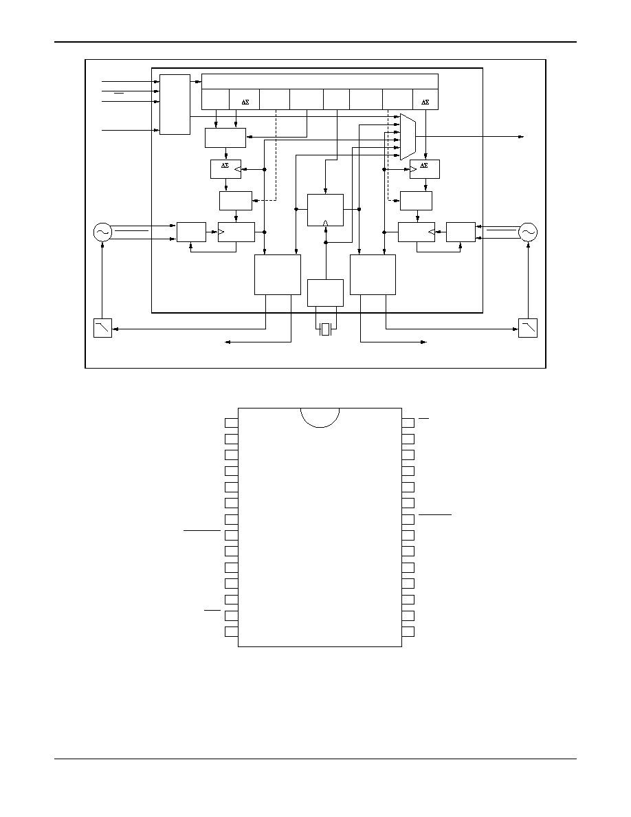
Figure 1 shows a functional block diagram for the CX72300. The device package
and pinout for the 28-pin Exposed Pad Thin Shrink Small Outline Package
(EP-TSSOP) are shown in Figure 2.
Distinguishing Features
∑
Spur-free operation
∑
2.1 GHz maximum operating frequency
∑
500 MHz maximum auxiliary synthesizer
∑
Ultra-fine step size, 100 Hz or less
∑
High internal reference frequency, up to 25 MHz,
which enables a larger loop bandwidth Phase
Locked Loop (PLL)
∑
Very fast switching speed (for example, below
100 ms)
∑
Phase noise to ≠91 dBc/Hz inside the loop filter
bandwidth @ 1800 MHz
∑
Software programmable power-down modes
∑
High-speed serial interface, up to 100 Mbps
∑
Three-wire programming
∑
Programmable division ratios on reference
frequency
∑
Phase detectors with programmable gain, which
provide a programmable loop bandwidth
∑
Frequency power steering further enhances rapid
acquisition time
∑
On-chip crystal oscillator
∑
Frequency adjust for temperature compensation
∑
Direct digital modulation
∑
3 V operation
∑
5 V output to loop filter
∑
28-pin EP-TSSOP
Applications
∑
General purpose RF systems
∑
2.5G and 3G wireless infrastructure
∑
Broadband wireless access
∑
Low bit rate wireless telemetry
∑
Instrumentation
∑
L-band receivers
∑
Satellite communications
CX72300
Frequency Synthesizer
2
Skyworks
101217F
Proprietary Information and Specifications Are Subject to Change
December 2, 2002
Serial
Interface
Modulation
Unit
Main
Divider
Auxiliary
Divider
Fvco_aux
Fvco_aux
Fvco_main
F
pd_main
F
pd_aux
F
ref_main
F
ref_aux
F
ref
CPout_aux
CPout_main
LD/PSmain
LD/PSaux
Fvco_main
Reference
Frequency
Oscillator
Reference
Frequency
Oscillator
Main
Phase/Freq.
Detector
and
Charge Pump
Auxiliary
Phase/Freq.
Detector
and
Charge Pump
Main
Divider
Auxiliary
Prescaler
Data
Mux
Mod_in
Mux_out
Clock
CS
Fractional
Unit
Fractional
Unit
18-Bit
10-Bit
Registers
Modul.
Data
Main
Div.
Modul.
Ctl
Ref.
Div.
Synth
Ctl
Aux.
Div.
Main
Aux.
Lock Detection or
Power Steering
Lock Detection or
Power Steering
C1411
Figure 1. CX72300 Functional Block Diagram
C1412
Clock
Mod_in
Mux_out
VSUBdigital
GNDcml
VCCcml_main
Fvco_main
Fvco_main
LD/PSmain
VCCcp_main
CPout_main
GNDcp_main
Xtalacgnd/OSC
Xtalin/OSC
CS
Data
VCCdigital
GNDdigital
VCCcml_aux
Fvco_aux
Fvco_aux
GNDcp_aux
CPout_aux
VCCcp_aux
LD/PSaux
GNDxtal
VCCxtal
Xtalout/NC
1
2
3
4
5
6
7
8
9
10
11
12
13
14
28
27
26
25
24
23
22
21
20
19
18
17
16
15
Figure 2. CX72300 Pinout, 28-Pin EP-TSSOP

Frequency Synthesizer
CX72300
101217F
Skyworks
3
December 2, 2002
Proprietary Information and Specifications Are Subject to Change
Technical Description
The CX72300 is supplied as a 28-pin EP-TSSOP. The exposed
pad is located on the bottom side of the package and must be
connected to ground for proper operation. The exposed pad
should be soldered directly to the circuit board. The device pinout
is shown in Figure 2.
The CX72300 is a fractional-N frequency synthesizer using a
≠
modulation technique. The fractional-N implementation provides
low in-band noise by having a low division ratio and fast
frequency settling time. In addition, the CX72300 provides
arbitrarily fine frequency resolution with a digital word, so that the
frequency synthesizer can be used to compensate for crystal
frequency drift in the RF transceiver.
Serial Interface _____________________________________
The serial interface is a versatile three-wire interface, consisting
of three pins: serial clock (Clock), serial input (Data), and chip
select (CS). It enables the CX72300 to operate in a system with
one or multiple masters and slaves. To perform a loopback test at
startup and to check the integrity of the board and processor, the
serial data is fed back to the master device (for example, a
microcontroller or microprocessor unit) through a programmable
multiplexer. This facilitates hardware and software debugging.
Registers__________________________________________
There are ten 16-bit registers in the CX72300.
Main and Auxiliary
Modulators_____________________
The fractionality of the CX72300 is accomplished by the use of a
proprietary, configurable 10-bit or 18-bit
modulator for the
main synthesizer and 10-bit
modulator for the auxiliary
synthesizer.
Main and Auxiliary Fractional Units ____________________
The CX72300 provides fractionality through the use of main and
auxiliary
modulators. The output from the main and auxiliary
modulators is combined with the main and auxiliary divider ratios
through their respective fractional units.
VCO Prescalers ____________________________________
The VCO prescalers provide low-noise signal conditioning of the
VCO signals. They translate from an off-chip single-ended or
differential signal to an on-chip differential Current Mode Logic
(CML) signal. The CX72300 has independent main and auxiliary
VCO prescalers.
Main and Auxiliary VCO Dividers ______________________
The CX72300 provides programmable dividers that control the
CML prescalers and supply the required signals to the charge
pump phase detectors. Programmable divide ratios ranging from
38 to 537 are possible in fractional-N mode and from 32 to 543 in
integer-N mode.
Reference Frequency Oscillator _______________________
The CX72300 has a self-contained, low-noise crystal oscillator.
This crystal oscillator is followed by the clock generation circuitry
that generates the required clock for the programmable reference
frequency dividers.
Reference Frequency Dividers ________________________
The crystal oscillator signal can be divided by a ratio of 1 to 32 to
create the reference frequencies for the phase detectors. The
CX72300 has both a main and an auxiliary frequency synthesizer,
and provides independently configurable dividers of the crystal
oscillator frequency for both the main and auxiliary phase
detectors. The divide ratios are programmed through the
Reference Frequency Dividers Register.
Note: The divided crystal oscillator frequencies (which are the
internal reference frequencies), F
ref_main
and F
ref_aux
, are
referred to as the reference frequencies throughout this
document.
Phase Detectors and Charge Pumps ___________________
The CX72300 uses a separate charge pump phase detector for
each synthesizer which provides a programmable gain, Kd, from
31.25 through 1000
µ
A/2
radians in 32 steps programmed via
the Control Register.
Frequency Steering _________________________________
When programmed for frequency power steering, the CX72300
has a circuit that helps the loop filter steer the VCO, through the
LD/PSmain pin. In this configuration, the LD/PSmain pin can
provide for more rapid acquisition.
When programmed for lock detection, internal frequency steering
is implemented and provides frequency acquisition times
comparable to conventional phase/frequency detectors.
Lock Detection _____________________________________
When programmed for lock detection, the CX72300 provides an
active low, pulsing open collector output on the LD/PSmain pin to
indicate the out-of-lock condition. When locked, the LD/PSmain
pin is three-stated (high impedance).
Power Down _______________________________________
The CX72300 supports a number of power-down modes through
the serial interface.

CX72300
Frequency Synthesizer
4
Skyworks
101217F
Proprietary Information and Specifications Are Subject to Change
December 2, 2002
Operation
This section describes the operation of the CX72300. The serial
interface is described first, followed by information on how to
obtain values for the Divide Ratio Registers.
Serial Interface _____________________________________
The serial interface consists of three pins: Clock, Data, and CS.
The Clock signal controls data transfers that synchronize and
sample the information on the two serial data lines (Data and CS).
The data pin bits shift into a temporary register on the rising edge
of Clock. The CS line allows individual selection of slave devices
on the same bus.
Figure 3 functionally depicts how a serial transfer takes place.
A serial transfer is initiated when a microcontroller or
microprocessor forces the CS line to a low state. This is
immediately followed by an address/data stream sent to the Data
pin that coincides with the rising edges of the clock presented on
the Clock line. Each rising edge of the Clock signal shifts in one
bit of data on the Data line into a shift register. At the same time,
one bit of data is shifted out of the Mux_out pin (if the serial bit
stream is selected) at each falling edge of Clock. To load any of
the synthesizer registers, 16 bits of address or data must be
presented to the Data line with the data LSB last while CS is low.
If CS is low for more than 16 clock cycles, only the last address or
data bits are used to load the synthesizer registers.
If the CS line is brought to a high state before the thirteenth clock
edge on Clock, the bit stream is assumed to be modulation data
samples. In this case, it is assumed that no address bits are
present and that all the bits in the stream should be loaded into
the Modulation Data Register.
Synthesizer Register Programming ____________________
Synthesizer register programming equations, described in this
section, use the following variables and constants:
N
fractional
Desired VCO division ratio in fractional-N applications.
This is a real number and can be interpreted as the
reference frequency (F
ref
) multiplying factor such that
the resulting frequency is equal to the desired VCO
frequency.
N
integer
Desired VCO division ratio in integer-N applications.
This number is an integer and can be interpreted as
the reference frequency (F
ref
) multiplying factor such
that the resulting frequency is equal to the desired
VCO frequency.
N
reg
9-bit unsigned input value to the divider ranging from 0
to 511 (integer-N mode) and from 6 to 505 (fractional-
N mode)
divider
This constant equals 262144 when the
modulator
is in 18-bit mode, and 1024 when the
modulator is
in 10-bit mode
dividend When in 18-bit mode, this is the 18-bit signed input
value to the
modulator, ranging from ≠131072 to
+131071 providing 262144 steps, each of
F
div_ref
/2
18
Hz.
When in 10-bit mode, this is the 10-bit signed input
value to the
modulator, ranging from ≠512 to +511
providing 1024 steps, each of F
div_ref
/2
10
Hz.
F
VCO
Desired VCO frequency (either F
vco_main
or F
vco_aux
).
F
div_ref
Divided reference frequency presented to the phase
detector
(either F
ref_main
or F
ref_aux
).
X
A3
A2
A1
A0
D11 D10 D9
D8
D7
D6
D5
D4
D3
D2
D1
D0
XXX
Clock
Last
Data
CS
C1413
Figure 3. Serial Transfer Timing Diagram

Frequency Synthesizer
CX72300
101217F
Skyworks
5
December 2, 2002
Proprietary Information and Specifications Are Subject to Change
Fractional-N Applications
The desired division ratio for the main and auxiliary synthesizers
is given by:
ref
_
div
VCO
fractional
F
F
N
=
where N
fractional
must be between 37.5 and 537.5 for the auxiliary
synthesizer. The value to be programmed in the Main or
Auxiliary Divider Register is given by:
32
)
N
(
Round
N
fractional
reg
-
=
Note: The Round function rounds the number to the nearest
integer.
When in fractional mode, allowed values for N
reg
are from 6 to
505 inclusive. The value to be programmed in the Main or
Auxiliary Dividend Register is given by:
)]
32
N
N
(
divider
[
Round
dividend
reg
fractional
-
-
◊
=
where the divider is either 1024 in 10-bit mode or 262144 in 18-
bit mode. Therefore, the dividend is a signed binary value either
10 or 18 bits long.
Note: Because of the high fractionality of the CX72300, there is
no practical need for any integer relationship between
the reference frequency and the channel spacing or
desired VCO frequencies.
Sample calculations for two fractional-N applications are
provided in Figure 4.
Integer-N Applications
The desired division ratio for the main or auxiliary synthesizer is
given by:
ref
_
div
main
_
vco
eger
int
F
F
N
=
where N
integer
is an integer number from 32 to 543 for both the
main and auxiliary synthesizers.
The value to be programmed in the Main or Auxiliary Divider
Register is given by:
32
N
N
eger
int
reg
-
=
When in integer mode, allowed values for N
reg
are from 0 to 511
for both the main and auxiliary synthesizers.
Note: As with all integer-N synthesizers, the minimum step size
is related to the crystal frequency and reference
frequency division ratio.
A sample calculation for an integer-N application is provided in
Figure 5.
Register Loading Order
In applications where the main synthesizer is in 18-bit mode, the
Main Dividend Most Significant Bit (MSB) Register holds the 10
MSBs of the dividend and the Main Dividend Least Significant
Bit (LSB) Register holds the 8 LSBs of the dividend. The
registers that control the main synthesizer's divide ratio are to
be loaded in the following order:
∑
Main Divider Register
∑
Main Dividend LSB Register
∑
Main Dividend MSB Register (at which point the new divide
ratio takes effect)
In applications where the main synthesizer is in 10-bit mode, the
Main Dividend MSB Register holds the 10 bits of the dividend.
The registers that control the main synthesizer's divide ratio are
to be loaded in the following order:
∑
Main Divider Register
∑
Main Dividend MSB Register (at which point the new divide
ratio takes effect)
For the auxiliary synthesizer, the Auxiliary Dividend Register
holds the 10 bits of the dividend. The registers that control the
auxiliary synthesizer's divide ratio are to be loaded in the
following order:
∑
Auxiliary Divider Register
∑
Auxiliary Dividend Register (at which point the new divide
ratio takes effect)
Note: When in integer mode, the new divide ratios take effect
as soon as the Main or Auxiliary Divider Register is
loaded.
Direct Digital Modulation _____________________________
The high fractionality and small step size of the CX72300 allow
the user to tune to practically any frequency in the VCO's
operating range. This frequency tuning allows direct digital
modulation by programming the different desired frequencies at
precise instants. Typically, the channel frequency is selected
through the Main Divider and Dividend Register and the
instantaneous frequency offset from the carrier is entered
through the Modulation Data Register.
The Modulation Data Register can be accessed in three ways,
which are defined in the following paragraphs.

CX72300
Frequency Synthesizer
6
Skyworks
101217F
Proprietary Information and Specifications Are Subject to Change
December 2, 2002
Case 1: To achieve a desired F
vco_main
frequency of 902.4530 MHz using a crystal frequency of 40 MHz with operation
of the synthesizer in 18-bit mode. Since the maximum internal reference frequency (F
div_ref
) is 25 MHz, the crystal
frequency is divided by 2 to obtain a F
div_ref
of 20 MHz. Therefore:
Nfractional = Fvco_main
Fdiv_ref
= 902.4530
20
= 45.12265
The value to be programmed in the Main Divider Register is:
Nreg = Round[Nfractional] ≠ 32
= Round[45.12265] ≠ 32
= 45 ≠ 32
= 13 (decimal)
= 000001101 (binary)
With the modulator in 18-bit mode, the value to be programmed in the Main Dividend Registers is:
dividend = Round[divider ◊ (Nfractional ≠ Nreg ≠ 32)]
= Round[262144 ◊ (45.12265 ≠ 13 ≠ 32)]
= Round[262144 ◊ (0.12265)]
= Round[32151.9616]
= 32152 (decimal)
= 000111110110011000 (binary)
where 00 0111 1101 is loaded in the MSB of the Main Dividend Register and 1001 1000 is loaded in the LSB of the
Main Dividend Register.
Summary:
∑
Main Divider Register = 0 0000 1101
∑
Main Dividend LSB Register = 1001 1000
∑
Main Dividend MSB Register = 00 0111 1101
∑
The resulting main VCO frequency is 902.453 MHz
∑
Step size is 76.3 Hz
Note: The frequency step size for this case is 20 MHz divided by 2
18
, giving 76.3 Hz.
C1414
Figure 4. Fractional-N Applications: Sample Calculation (1 of 2)

Frequency Synthesizer
CX72300
101217F
Skyworks
7
December 2, 2002
Proprietary Information and Specifications Are Subject to Change
Case 2: To achieve a desired F
vco_main
frequency of 917.7786 MHz using a crystal frequency of 19.2 MHz with operation
of the synthesizer in 10-bit mode. Since the maximum internal reference frequency (F
div_ref
) is 25 MHz, the crystal
frequency does not require the internal division to be greater than 1, which makes F
div_ref
= 19.2 MHz. Therefore:
Nfractional = Fvco_main
Fdiv_ref
= 917.7786
19.2
= 47.80097
The value to be programmed in the Main Divider Register is:
Nreg = Round[Nfractional] ≠ 32
= Round[47.80097] ≠ 32
= 48 ≠ 32
= 16 (decimal)
= 000010000 (binary)
With the modulator in 10-bit mode, the value to be programmed in the Main Dividend Registers is:
dividend = Round[divider ◊ (Nfractional ≠ Nreg ≠ 32)]
= Round[1024 ◊ (47.80097 ≠ 16 ≠ 32)]
= Round[1024 ◊ (≠ 0.1990312)]
= Round[≠ 203.808]
= 204 (decimal)
= 1100110100 (binary)
where 11 0011 0100 is loaded in the MSB of the Main Dividend Register.
Summary:
∑
Main Divider Register = 0 0001 0000
∑
Main Dividend MSB Register = 11 0011 0100
∑
The resulting main VCO frequency is 917.775 MHz
∑
Step size is 18.75 kHz
Note: The frequency step size for this case is 19.2 MHz divided by 2
10
, giving 18.75 kHz.
C1415
Figure 4. Fractional-N Applications: Sample Calculation (2 of 2)

CX72300
Frequency Synthesizer
8
Skyworks
101217F
Proprietary Information and Specifications Are Subject to Change
December 2, 2002
To achieve a desired F
vco_aux
frequency of 400 MHz using a crystal frequency of 16 MHz. Since the minimum
divide ratio is 32, the reference frequency (F
div_ref
) must be a maximum of 12.5 MHz. Choosing a reference
frequency divide ratio of 2 provides a reference frequency of 8 MHz. Therefore:
Ninteger
= Fvco_aux
Fdiv_ref
=
400
8
=
50
The value to be programmed in the Auxiliary Divider Register is:
Nreg = Ninteger ≠ 32
= 50 ≠ 32
= 18 (decimal)
= 000010010 (binary)
Summary:
∑
Auxiliary Divide Register = 0 0001 0010
C1416
Figure 5. Integer-N Applications: Sample Calculation
Normal Register Write. A normal 16-bit serial interface write
occurs when CS is 16 clock cycles wide. The corresponding
16-bit modulation data is simultaneously presented to the Data
pin. The content of the Modulation Data Register is passed to
the modulation unit at the next falling edge of the divided main
VCO frequency (F
pd_main
).
Short CS Through Data Pin (No Address Bits Required). A
shortened serial interface write occurs when CS is from 2 to 12
clock cycles wide. The corresponding modulation data (2 to 12
bits) is simultaneously presented to the Data pin. The Data pin is
the default pin used to enter modulation data directly in the
Modulation Data Register with shortened CS strobes. This
method of data entry eliminates the register address overhead
on the serial interface. All serial interface bits are re-
synchronized internally at the reference oscillator frequency.
The content of the Modulation Data Register is passed to the
modulation unit at the next falling edge of the divided main VCO
frequency (F
pd_main
).
Short CS Through Mod_in Pin (No Address Bits Required).
A shortened serial interface write occurs when CS is from 2 to
12 clock cycles wide. The corresponding modulation data (2 to
12 bits) is simultaneously presented on the Mod_in pin. The
Mod_in pin is the alternate pin used to enter modulation data
directly into the Modulation Data Register with shortened CS
strobes. This mode is selected through the Modulation Control
Register. This method of data entry also eliminates the register
address overhead on the serial interface and allows a different
device than the one controlling the channel selection to enter
the modulation data (e.g., a microcontroller for channel selection
and a digital signal processor for modulation data). All serial
interface bits are re-synchronized internally at the reference
oscillator frequency and the content of the Modulation Data
Register is passed to the modulation unit at the next falling edge
of the divided main VCO frequency (F
pd_main
).
Modulation data samples in the Modulation Data Register can
be from 2 to 12 bits long, and enable the user to select how
many distinct frequency steps are to be used for the desired
modulation scheme.
The user can also control the frequency deviation through the
modulation data magnitude offset in the Modulation Control
Register. This allows shifting of the modulation data to
accomplish a 2
m
multiplication of frequency deviation.
The programmable range of ≠0.5 to +0.5 of the main
modulator can be exceeded up to the condition where the sum
of the dividend and the modulation data conform to:
5625
.
0
)
dividend
N
(
5625
.
0
mod
+
+
-
When the sum of the dividend and modulation data lie outside
this range, the value of N
integer
must be changed.
For a more detailed description of direct digital modulation
functionality, refer to the Skyworks document CX72300/1/2
Direct Digital Modulation Application Note, document number
101349.
Frequency Synthesizer
CX72300
101217F
Skyworks
9
December 2, 2002
Proprietary Information and Specifications Are Subject to Change
Table 1. CX72300 Register Map
Address (Hex)
Register (Note 1)
Length (Bits)
Address (Bits)
0
Main Divider Register
12
4
1
Main Dividend MSB Register
12
4
2
Main Dividend LSB Register
12
4
3
Auxiliary Divider Register
12
4
4
Auxiliary Dividend Register
12
4
5
Reference Frequency Dividers Register
12
4
6
Control Register--phase detector/charge pumps
12
4
7
Control Register--power down/multiplexer output select
12
4
8
Modulation Control Register
12
4
9
--
Modulation Data Register
Modulation Data Register (Note 2) -- direct input
12
2
length
12 bits
4
0
Note 1: All registers are write only.
Note 2: No address bits are required for modulation data. Any serial data between 2 and 12 bits long is considered modulation data.
A3
A2 A1
A0 11
10
9
8
7
6
5
4
3
2
1
0
0
0
0
0
X
X
X
MSB
LSB
Main Synthesizer Divider Index
C1417
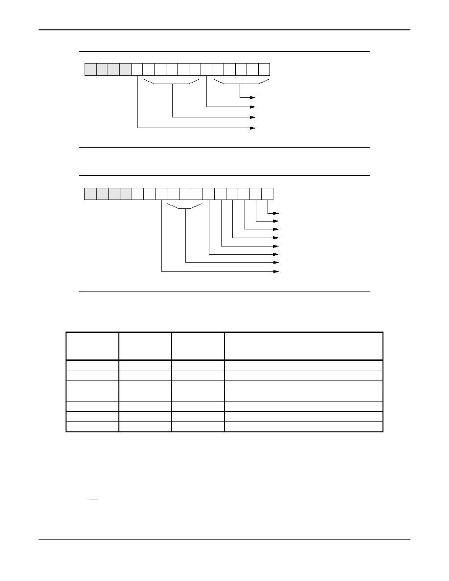
Figure 6. Main Divider Register (Write Only)
Registers
This section describes the CX72300 registers. All register writes
are programmed address first, followed directly with data. MSBs
are entered first. On power-up, all registers are reset to 0x000
except registers at addresses 0x0 and 0x3, which are set to
0x006. Table 1 provides a description for each of the CX72300
device registers.
Synthesizer Registers _______________________________
Main Synthesizer Registers. The Main Divider Register
contains the integer portion closest to the desired fractional-N
(or the integer-N) value minus 32 for the main synthesizer. This
register, in conjunction with the Main Dividend Registers (which
control the fraction offset from
≠
0.5 to +0.5), allows selection of
a precise frequency. As shown in Figure 6, the value to be
loaded is:
∑
Main Synthesizer Divider Index = 9-bit value for the integer
portion of the main synthesizer dividers. Valid values for
this register are from 6 to 505 (fractional-N) or from 0 to
511 (integer-N).
The Main Dividend MSB and LSB Registers control the fraction
part of the desired fractional-N value and allow an offset of
≠
0.5
to +0.5 to the main integer selected through the Main Divider
Register. As shown in Figures 7 and 8, values to be loaded are:
∑
Main Synthesizer Dividend (MSBs) = 10-bit value for the
MSBs of the 18-bit dividend for the main synthesizer.
∑
Main Synthesizer Dividend (LSBs) = 8-bit value for the
LSBs of the 18-bit dividend for the main synthesizer.
The Main Dividend Register MSB and LSB values are 2's
complement format.
Note: When in 10-bit mode, the Main Synthesizer Dividend
(LSBs) is not required.
CX72300
Frequency Synthesizer
Data Sheet
Skyworks
Doc. No. 101217F
Proprietary Information and Specifications Are Subject to Change
December 2, 2002
C1418
A3
A2 A1
A0 11
10
9
8
7
6
5
4
3
2
1
0
0
0
0
1
X
X
MSB
LSB
Main Synthesizer Dividend (MSBs)
Figure 7. Main Dividend MSB Register (Write Only)
A3
A2 A1
A0
11
10
9
8
7
6
5
4
3
2
1
0
0
0
1
0
X
X
X
X
MSB
LSB
Main Synthesizer Dividend (LSBs)
C1419
Figure 8. Main Dividend LSB Register (Write Only)
A3
A2 A1
A0
11
10
9
8
7
6
5
4
3
2
1
0
0
0
1
1
X
X
X
MSB
LSB
Auxiliary Synthesizer Divider Index
C1420
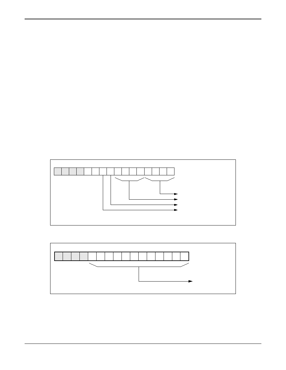
Figure 9. Auxiliary Divider Register (Write Only)
A3
A2 A1
A0
11
10
9
8
7
6
5
4
3
2
1
0
0
1
0
0
X
X
MSB
LSB
Auxiliary Synthesizer Dividend
C1421
Figure 10. Auxiliary Dividend Register (Write Only
Auxiliary Synthesizer Registers. The Auxiliary Divider
Register contains the integer portion closest to the desired
fractional-N (or integer-N) value minus 32 for the auxiliary
synthesizer. This register, in conjunction with the Auxiliary
Dividend Register, which controls the fraction offset (from
≠
0.5
to +0.5), allows selection of a precise frequency. As shown in
Figure 9, the value to be loaded is:
∑
Auxiliary Synthesizer Divider Index = 9-bit value for the
integer portion of the auxiliary synthesizer dividers. Valid
values for this register are from 6 to 505 (fractional-N) or
from 0 to 511 (integer-N).
The Auxiliary Dividend Register controls the fraction part of the
desired fractional-N value and allows an offset of
≠
0.5 to +0.5 to
the auxiliary integer selected through the Auxiliary Divider
Register. As shown Figure 10, the value to be loaded is:
∑
Auxiliary Synthesizer Dividend = 10-bit value for the
dividend for the auxiliary synthesizer.
General Synthesizer Registers. The Reference Frequency
Dividers Register configures the dual-programmable reference
frequency dividers for the main and auxiliary synthesizers.
The dual-programmable reference frequency dividers provide
the reference frequencies to the phase detectors by dividing the
Frequency Synthesizer
CX72300
101217F
Skyworks
11
December 2, 2002
Proprietary Information and Specifications Are Subject to Change
crystal oscillator frequency. The lower five bits hold the
reference frequency divide index for the main phase detector.
The next five bits hold the reference frequency divide index for
the auxiliary phase detector. Divide ratios from 1 to 32 are
possible for each reference frequency divider. As shown in
Figure 11, the values to be loaded are:
∑
Main Reference Frequency Divider Index = Desired main
oscillator frequency division ratio
≠
1. Default value on
power-up is 0, signifying that the reference frequency is not
divided for the main phase detector. See Table 2 for other
programming values.
∑
Auxiliary Reference Frequency Divider Index = Desired
auxiliary oscillator frequency division ratio
≠
1. Default value
on power-up is 0, signifying that the reference frequency is
not divided for the auxiliary phase detector. See Table 3 for
other programming values.
A3
A2 A1
A0 11
10
9
8
7
6
5
4
3
2
1
0
0
1
0
1
X
X
Main Reference Frequency Divider Index
Auxiliary Reference Frequency Divider Index
C1422
Figure 11. Reference Frequency Dividers Register (Write Only)
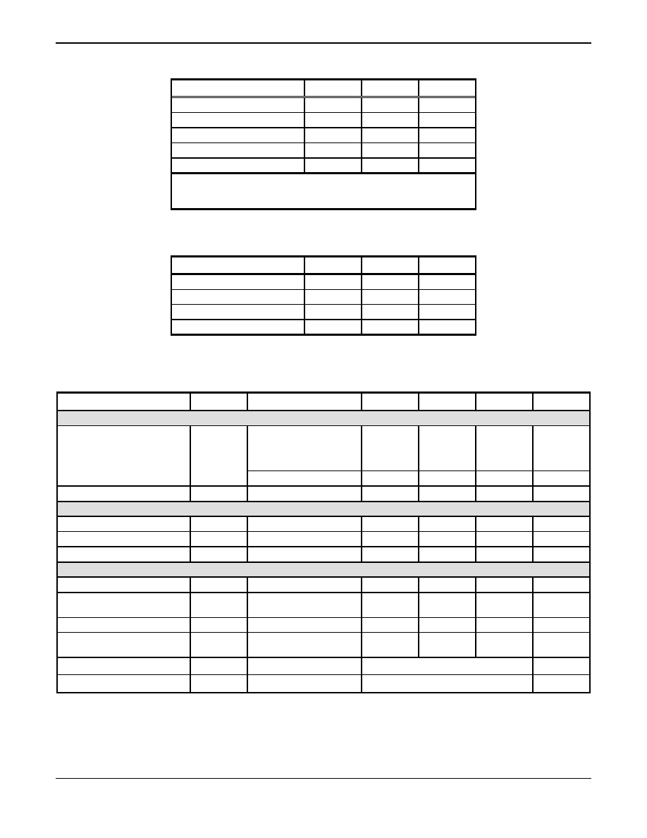
Table 2. Programming the Main Reference Frequency Divider
Decimal
Bit 4 (MSB)
Bit 3
Bit 2
Bit 1
Bit 0 (LSB)
Reference
Divider Ratio
0
0 0 0 0 0 1
1
0 0 0 0 1 2
2
0 0 0 1 0 3
≠
≠ ≠ ≠ ≠ ≠ ≠
≠
≠ ≠ ≠ ≠ ≠ ≠
≠
≠ ≠ ≠ ≠ ≠ ≠
31
1 1 1 1 1 32
Table 3. Programming the Auxiliary Reference Frequency Divider
Decimal
Bit 9 (MSB)
Bit 8
Bit 7
Bit 6
Bit 5 (LSB)
Reference
Divider Ratio
0
0 0 0 0 0 1
1
0 0 0 0 1 2
2
0 0 0 1 0 3
≠
≠ ≠ ≠ ≠ ≠ ≠
≠
≠ ≠ ≠ ≠ ≠ ≠
≠
≠ ≠ ≠ ≠ ≠ ≠
31
1 1 1 1 1 32

CX72300
Frequency Synthesizer
12
Skyworks
101217F
Proprietary Information and Specifications Are Subject to Change
December 2, 2002
The Control Register allows control of the gain for both phase
detectors and configuration of the LD/PSmain and LD/PSaux
pins for frequency power steering or lock detection. As shown in
Figure 12, the values to be loaded are:
∑
Main Phase Detector Gain = 5-bit value for programmable
main phase detector gain. Range is from 0 to 31 decimal
for 31.25 to 1000
µ
A/ 2
radian, respectively.
∑
Main Power Steering Enable = 1-bit value to enable the
frequency power steering circuitry of the main phase
detector. When this bit is a 0, the LD/PSmain pin is
configured to be a lock detect, active low, open collector
pin. When this bit is a 1, the LD/PSmain pin is configured to
be a frequency power steering pin and can be used to
bypass the external main loop filter to provide faster
frequency acquisition.
∑
Auxiliary Phase Detector Gain = 5-bit value for
programmable auxiliary phase detector gain. Range is from
0 to 31 decimal for 31.25 to 1000
µ
A/2
radians,
respectively.
∑
Auxiliary Power Steering Enable = 1-bit value to enable the
frequency power steering circuitry of the auxiliary phase
detector. When this bit is a 0, the LD/PSaux pin is
configured to be a lock detect, active low, open collector
pin. When this bit is a 1, the LD/PSaux is configured to be a
frequency power steering pin and may be used to bypass
the external auxiliary loop filter to provide faster frequency
acquisition.
The Power Down and Multiplexer Output Register allows control
of the power-down modes, internal multiplexer output, and main
synthesizer fractionality. As shown in Figure 13, the values
to be loaded are:
∑
Full Power Down = 1-bit value that powers down the
CX72300 except for the reference oscillator and the serial
interface. When this bit is 0, the CX72300 is powered up.
When this bit is 1, the CX72300 is in full power-down mode
excluding the Mux_out pin.
∑
Main Synthesizer Power Down = 1-bit value that powers
down the main synthesizer. When this bit is 0, the main
synthesizer is powered up. When this bit is 1, the main
synthesizer is in power-down mode.
∑
Main Synthesizer Mode = 1-bit value that powers down the
main synthesizer's
modulator and fractional unit to
operate as an integer-N synthesizer. When this bit is 0, the
main synthesizer is in fractional-N mode. When this bit is 1,
the main synthesizer is in integer-N mode.
∑
Main Synthesizer
Fractionality = 1-bit value that
configures the size of the main
modulator. This has a
direct effect on power consumption and on the level of
fractionality and step size. When this bit is 0, the main
modulator is 18-bit with a fractionality of 2
18
and a step size
of F
ref_main
/262144. When this bit is 1, the main
modulator is 10-bit with a fractionality of 2
10
and a step size
of F
ref_main
/1024.
∑
Auxiliary Synthesizer Power Down = 1-bit value that
powers down the auxiliary synthesizer. When this bit is 0,
the auxiliary synthesizer is powered up. When this bit is 1,
the auxiliary synthesizer is in power-down mode.
∑
Auxiliary Synthesizer Mode = 1-bit value that powers down
the auxiliary synthesizer's
modulator and fractional unit
to operate as an integer-N synthesizer. When this bit is 0,
the auxiliary synthesizer is in fractional-N mode. When this
bit is 1, the auxiliary synthesizer is in integer-N mode.
Note: There are no special power-up sequences required for
the CX72300.
∑
Multiplexer Output Selection = 3-bit value that selects
which internal signal is output to the Mux_out pin. The
following internal signals are available on this pin:
-
Reference Oscillator: F
ref
-
Main or auxiliary divided reference (post reference
frequency main or auxiliary dividers): F
ref_main
or F
ref_aux
-
Main or auxiliary phase detector frequency (post main
and auxiliary frequency dividers): F
pd_main
or F
pd_aux
-
Serial data out for loop-back and test purposes
∑
Mux_out Pin Three-State Enable = 1-bit value to three-
state the Mux_out pin. When this bit is 0, the Mux_out pin
is enabled. When this bit is 1, the Mux_out pin is three-
stated.
Refer to Table 4 for more information.
Frequency Synthesizer
CX72300
101217F
Skyworks
13
December 2, 2002
Proprietary Information and Specifications Are Subject to Change
A3
A2 A1
A0 11
10
9
8
7
6
5
4
3
2
1
0
0
1
1
0
Main Phase Detector Gain
Main Power Steering/Lock Detect Enable
Auxiliary Phase Detector Gain
Auxiliary Power Steering/Lock Detect Enable
C1423
Figure 12. Control Register (Write Only)
A3
A2 A1
A0 11
10
9
8
7
6
5
4
3
2
1
0
0
1
1
1
X
X
MSB
LSB
Full Power Down
Main Synthesizer Power Down
Main Synthesizer Mode
Main Synthesizer
Fractionality
Auxiliary Synthesizer Power Down
Auxiliary Synthesizer Mode
Multiplexer Output Selection
Mux_out Pin Three-State Enable
C1424
Figure 13. Power Down and Multiplexer Output Register (Write Only)
Table 4. Multiplexer Output
Multiplexer
Output Select
(Bit 8)
Multiplexer
Output Select
(Bit 7)
Multiplexer
Output Select
(Bit 6)
Multiplexer Output (Mux_out)
0 0 0
Reference
oscillator
0 0 1
Auxiliary
reference
frequency
(F
ref_aux
)
0 1 0
Main
reference
frequency
(F
ref_main
)
0 1 1
Auxiliary
phase
detector
frequency
(F
pd_aux
)
1 0 0
Main
phase
detector
frequency
(F
pd_main
)
1 0 1
Serial
data
out
1
1
0
Serial interface register test output
The Modulation Control Register is used to configure the
modulation unit of the main synthesizer.
The modulation unit adds or subtracts a frequency offset to the
selected center frequency at which the main synthesizer
operates. The size of the modulation data sample, controlled by
the duration of the CS pin, can be from 2 to 12 bits wide to
provide from 4 to 4096 selectable frequency offset steps.
The modulation data magnitude offset selects the magnitude
multiplier for the modulation data and can be from 0 to 8.
As shown in Figure 14, the values to be loaded are:
∑
Modulation Data Magnitude Offset = 4-bit value that
indicates the magnitude multiplier (m) for the modulation
data samples. Valid values range from 0 to 13, effectively
providing a 2
m
multiplication of the modulation data sample.
CX72300
Frequency Synthesizer
14
Skyworks
101217F
Proprietary Information and Specifications Are Subject to Change
December 2, 2002
∑
Modulation Data Input Select = 1-bit value that indicates
the pin on which modulation data samples are serially input
when the CS signal is between 2 and 12 bits long. When
this bit is 0, modulation data samples are to be presented
on the Data pin. When this bit is 1, modulation data
samples are to be presented on the Mod_in pin.
∑
Modulation Address Disable = 1-bit value that indicates the
presence of the address as modulation data samples are
presented on either the Mod_in or Data pins. When this bit
is 0, the address is presented with the modulation data
samples (i.e., all transfers are 16 bits long). When this bit is
1, no address is presented with the modulation data
samples (i.e., all transfers are 2 to 12 bits long).
The Modulation Data Register loads the modulation data
samples to the modulation unit. This value is transferred to the
modulation unit on the falling edge of F
pd_main
where it is passed
to the main
modulator at the selected magnitude offset on
the next falling edge of F
pd_main
. Modulation Data Register values
are 2's complement format.
As shown in Figure 15, the value to be loaded is:
∑
Modulation Data Bits = Modulation data samples that
represent the instantaneous frequency offset to the
selected main synthesizer frequency (selected channel)
before being affected by the modulation data magnitude
offset.
Electrical and Mechanical Specifications
Signal pin assignments and functional pin descriptions are
described in Table 5. The absolute maximum ratings of the
CX72300 are provided in Table 6. The recommended operating
conditions are specified in Table 7 and electrical specifications
are provided in Table 8.
Figure 16 provides a schematic diagram for the CX72300.
Figure 17 shows the package dimensions for the 28-pin
EP-TSSOP and Figure 18 provides the tape and reel
dimensions.
Electrostatic Discharge (ESD) Sensitivity
The CX72300 is a static-sensitive electronic device. Do not
operate or store near strong electrostatic fields. Take proper
ESD precautions.
A3
A2 A1
A0 11
10
9
8
7
6
5
4
3
2
1
0
1
0
0
0
0
0
0
0
X
X
Reserved Bits
Modulation Data Magnitude Offset
Modulation Data Input Select
Modulation Address Disable
C1425
Figure 14. Modulation Control Register (Write Only)
A3
A2 A1
A0
11
10
9
8
7
6
5
4
3
2
1
0
1
0
0
1
MSB
LSB
Modulation Data Bits
C1426
Figure 15. Modulation Data Register (Write Only)

Frequency Synthesizer
CX72300
101217F
Skyworks
15
December 2, 2002
Proprietary Information and Specifications Are Subject to Change
Table 5. CX72300 Signal Descriptions
Pin #
Name
Type
Description
1
Clock
Digital input
Clock signal pin. When CS is low, the register address and data are shifted in address bits first
on the Data pin on the rising edge of Clock.
2
Mod_in
Digital input
Alternate serial modulation data input pin. Address bits are followed by data bits.
3
Mux_out
Digital output
Internal multiplexer output. Selects from oscillator frequency, main or auxiliary reference
frequency, main or auxiliary divided VCO frequency, serial data out, or testability signals. This
pin can be three-stated from the general synthesizer registers.
4
VSUBdigital
≠
Substrate isolation. Connect to ground.
5
GNDecl/cml (Note 1)
Power and ground
Emitter Coupled Logic (ECL)/Current Mode Logic (CML) ground.
6 VCCcml_main
(Note 1)
Power and ground
ECL/CML 3 V. Removing power safely powers down the associated divider chain and charge
pump.
7
Fvco_main
Input
Main VCO differential input.
8
Fvco_main
Input
Main VCO complimentary differential input.
9
LD/PSmain
Analog output
Programmable output pin. Indicates main phase detector out-of-lock as an active low pulsing
open collector output (high impedance when lock is detected), or helps the loop filter steer the
main VCO. This pin is configured from the general synthesizer registers.
10
VCCcp_main (Note 1) Power and ground
Main charge pump 3 to 5 V. Removing power safely powers down the associated divider chain
and charge pump.
11
CPout_main
Analog output
Main charge pump output. The gain of the main charge pump phase detector can be controlled
from the general synthesizer registers.
12 GNDcp_main
(Note 1)
Power and ground
Main charge pump ground.
13
Xtalacgnd/OSC
Ground/input
Reference crystal AC ground or external oscillator differential input.
14
Xtalin/OSC
Input
Reference crystal input or external oscillator differential input.
15
Xtalout/NC
Input
Reference crystal output or no connect.
16
VCCxtal
Power and ground
Crystal oscillator ECL/CML 3 V.
17
GNDxtal
Power and ground
Crystal oscillator ground.
18
LD/PSaux
Analog output
Programmable output pin. Indicates auxiliary phase detector out-of-lock as an active low pulsing
open collector output (high impedance when lock is detected), or helps the loop filter steer the
auxiliary VCO. This pin is configured from the general synthesizer registers.
19
VCCcp_aux (Note 1) Power and ground
Auxiliary charge pump 3 to 5 V. Removing power safely powers down the associated divider
chain and charge pump.
20
CPout_aux
Analog output
Auxiliary charge pump output. The gain of the auxiliary charge pump phase detector can be
controlled from the general synthesizer registers.
21 GNDcp_aux
(Note 1)
Power and ground
Auxiliary charge pump ground.
22
Fvco_aux
Input
Auxiliary VCO complimentary differential input.
23
Fvco_aux
Input
Auxiliary VCO differential input.
24 VCCcml_aux
(Note 1)
Power and ground
ECL/CML 3 V. Removing power safely powers down the associated divider chain and charge
pump.
25
GNDdigital (Note 1)
Power and ground
Digital ground.
26
VCCdigital (Note 1)
Power and ground
Digital 3 V.
27
Data
Digital input
Serial address and data input pin. Address bits are followed by data bits.
28
CS
Digital input
Active low enable pin. Enables loading of address and data on the Data pin on the rising edge
of Clock. When CS goes high, data is transferred to the register indicated by the address.
Subsequent clock edges are ignored.
Note 1: Associated pairs of power and ground pins must be decoupled using 0.1
µ
F capacitors.
CX72300
Frequency Synthesizer
16
Skyworks
101217F
Proprietary Information and Specifications Are Subject to Change
December 2, 2002
Table 6. Absolute Maximum Ratings
Parameter Min
Max
Units
Maximum analog RF supply voltage
3.6
VDC
Maximum digital supply voltage
3.6
VDC
Maximum charge pump supply voltage
5.25
VDC
Storage temperature
≠65
+150
∞C
Operating temperature
≠40
+85
∞C
Note: Exposure to maximum rating conditions for extended periods may reduce device
reliability. There is no damage to device with only one parameter set at the limit and all
other parameters set at or below their nominal conditions.
Table 7. Recommended Operating Conditions
Parameter Min
Max
Units
Analog RF supplies
2.7
3.3
VDC
Digital supply
2.7
3.3
VDC
Charge pump supplies
2.7
5.0
VDC
Operating temperature (T
A
) ≠40
+85
∞C
Table 8. Electrical Characteristics (1 of 2)
(VDD = 3 V, T
A
= 25
∞
∞
∞
∞
C, unless otherwise noted)
Parameter Symbol
Test
Conditions
Min
Typical
Max
Units
Power Consumption
Total power consumption
P
TOTAL
Charge pump currents of 200
µ
A.
Both synthesizers fractional,
F
REF
_
MAIN
= 20 MHz,
F
REF
_
AUX
= 1 MHz
37.5 mW
Auxiliary
synthesizer
power-down
27 mW
Power-down current
I
CC
_
PWDN
10
(Note
1)
µ
A
Reference Oscillator
Reference oscillator frequency
F
OSC
50 MHz
Oscillator sensitivity (as a buffer)
V
OSC
AC
coupled,
single-ended
0.1 2.0 Vp-p
Frequency shift versus supply voltage
F
SHIFT
_
SUPPLY
2.7 V
V
XTAL
3.3 V
±
0.3
ppm
VCOs
Main synthesizer operating frequency
Fvco_main
Sinusoidal, ≠40
∞
C to +85
∞
C
100 (Note 2)
2100
MHz
Auxiliary synthesizer operating
frequency
Fvco_aux
Sinusoidal, ≠40
∞
C to +85
∞
C
100 (Note 2)
500
MHz
RF input sensitivity
V
VCO
AC
coupled
50
250 mVpeak
RF input impedance
Z
VCO
_
IN
94 ≠ j140 @
1200 MHz
Main fractional-N tuning step size
F
STEP
_
MAIN
F
REF
_
MAIN
/2
18
or F
REF
_
MAIN
/2
10
Hz
Auxiliary fractional-N tuning step size
F
STEP
_
AUX
F
REF
_
AUX
/2
10
Hz

Frequency Synthesizer
CX72300
101217F
Skyworks
17
December 2, 2002
Proprietary Information and Specifications Are Subject to Change
Table 8. Electrical Characteristics (2 of 2)
(VDD = 3 V, T
A
= 25
∞
∞
∞
∞
C, unless otherwise noted)
Parameter Symbol
Test
Conditions
Min
Typical
Max
Units
Noise
Phase noise floor
P
NF
Measured inside the loop
bandwidth using 25 MHz
reference frequency,
≠40
∞
C to +85
∞
C
≠128
+
20Log(N)
dBc/Hz
Phase Detectors and Charge Pumps
Main phase detector frequency
F
REF
_
MAIN
≠40
∞
C to +85
∞
C
25
MHz
Auxiliary phase detector frequency
F
REF
_
AUX
≠40
∞
C to +85
∞
C
25
MHz
Charge pump output source current
I
CP
_
SOURCE
V
CP
= 0.5 x VCC
CP
125
1000
µ
A/2
Charge pump output sink current
I
CP
_
SINK
V
CP
= 0.5 x VCC
CP
≠125
≠1000
µ
A/2
Charge pump accuracy
I
CP
_
ACCURACY
±
20
%
Charge pump output voltage linearity
range
I
CP
vs. V
CP
0.5 V
V
CP
(VCC
CP
≠ 0.5 V)
GND + 400
VCC
CP
≠ 400
mV
Charge pump current versus
temperature
I
CP
vs. T
V
CP
= 0.5 VCC
CP
,
≠40
∞
C < T < +85
∞
C
5
%
Charge pump current versus voltage
I
CP
vs. V
CP
0.5 V
V
CP
(VCC
CP
≠ 0.5 V)
8
%
Digital Pins
High level input voltage
VIH
0.7 V
DIGITAL
V
Low level input voltage
VIL
0.3 V
DIGITAL
V
High level output voltage
VOH
I
OH
= ≠2 mA
V
DIGITAL
≠ 0.2
V
Low level output voltage
VOL
I
OL
= 2 mA
GND + 0.2
V
Timing ≠ Serial Interface
Clock frequency
f
CLOCK
100 MHz
Data and CS set-up time to Clock rising t
SU
3 ns
Data and CS hold time after Clock rising t
HOLD
0
ns
Note 1: A 5 V charge pump power supply (on pin 10 and/or pin 19) results in higher power-down leakage current.
Note 2: When operating in fractional mode, minimum synthesizer frequency is 12 x Fosc, where Fosc is the frequency at the Xtalin/OSC pin.
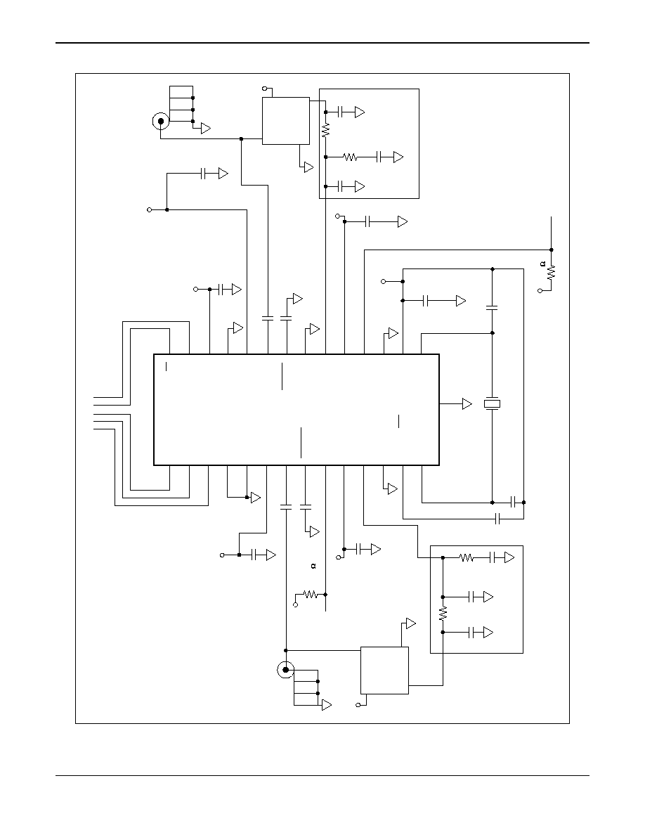
CX72300
F
r
equenc
y
Sy
nthes
i
z
er
18
Skyworks
101217F
Propri
e
tary
Informati
on and Spec
i
f
i
c
ati
ons
Are Subj
ec
t to Change
Dec
e
mber 2, 2002
Clock
Mod_in
Mux_out
VSUBdigital
GNDecl/cml
VCCcml_main
Fvco_main
Fvco_main
LD/PSmain
VCCcp_main
CPout_main
GNDcp_main
Xtalacgnd/OSC
Xtalin/OSC
CS
Data
VCCdigital
GNDdigital
VCCcml_aux
Fvco_aux
Fvco_aux
GNDcp_aux
CPout_aux
VCCcp_aux
LD/PSaux
GNDxtal
VCCxtal
Xtalout/NC
1
2
3
4
5
6
7
8
9
10
11
12
13
14
28
27
26
25
24
23
22
21
20
19
18
17
16
15
GND
29
To Microprocessor
3 V
3 V
3 V
VCC
3 V
3 V
3 V
3 V
3 V
C5
C7
1
1
5
4
4
3
3
2
2
RF Out Main
J1
1
1
5
4
4
3
3
2
2
RF Out Auxiliary
J1
Main VCO
Y1
Main Synthesizer Loop Filter
Auxiliary Synthesizer Loop Filter
Auxiliary
VCO
Auxiliary
VCO
External Pad
Connection to
Ground
GND
VCC
C14
R4
R6
100 k
R5
C15
C8
GND
VT
VCC
RFOUT
C12
C9
C4
C6
R3
R2
C19
C18
C17
C17
1 nF
VCC
RFOUT
VT
Lock Detect
Main Output
Lock Detect
Auxiliary Output
A
A
A
A
A
A
A
A
A
A
A
A
C10
1 nF
A
A
A
A
A
A
A
A
A
A
A
A
R1
100 k
C3
1 nF
C11
1 nF
C2
1 nF
C1
1 nF
C16
100 pF
C1427
F
i
g
u
r
e 16. CX72300 Ap
p
licatio
n
Sch
e
m
a
tic
Frequency Synthesizer
CX72300
101217F
Skyworks
19
December 2, 2002
Proprietary Information and Specifications Are Subject to Change
b
e
1
E
1
E
TOP VIEW
SIDE VIEW DETAIL
EXPOSED PAD BOTTOM VIEW
P
1
P
A
A
1
A
2
L
A
A
1
A
2
D
E
E
1
L
P
P
1
e
b
0.05
0.85
4.30
0.50
0.19
1.10
0.15
0.95
4.50
0.70
3.50
3.00
0.30
9.70 BSC
6.40 BSC
0.65 BSC
D
MIN.
Millimeters
Dim.
MAX.
C1428
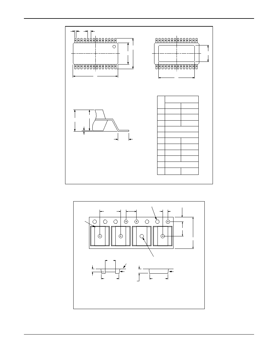
Figure 17. CX72300 28-Pin EP-TSSOP Package Dimension Drawing
0.318 ± 0.013
1.10
3.96
6.75 ± 0.10
8o Max
7o Max
1.60 ± 0.10
9.95 ± 0.10
1.50 ± 0.25
16.00 +0.30/≠0.10
7.50 ± 0.10
8.00 ± 0.10
4.00 ± 0.10
2.00
± 0.05
1.75 ± 0.10
1.50 ± 0.10
Pin #1
indicator
NOTE(S):
1. Carrier tape material: black conductive polycarbonate
2. Cover tape material: transparent conductive PSA
3. Cover tape size: 13.3 mm width
4. Tolerance: .XX = ±0.10
5. All measurements are in millimeters
C1430
Figure 18. CX72300 Tape and Reel Dimensions

CX72300
Frequency Synthesizer
20
Skyworks
101217F
Proprietary Information and Specifications Are Subject to Change
December 2, 2002
Ordering Information
Model Name
Ordering Part Number
Evaluation Kit Part
Number
CX72300 Frequency Synthesizer
CX72300-11
PH00-D112
© 2001, 2002, Skyworks Solutions, Inc. All Rights Reserved.
Information in this document is provided in connection with Skyworks Solutions, Inc. ("Skyworks") products. These materials are provided by Skyworks as a service to its
customers and may be used for informational purposes only. Skyworks assumes no responsibility for errors or omissions in these materials. Skyworks may make changes to
its products, specifications and product descriptions at any time, without notice. Skyworks makes no commitment to update the information and shall have no responsibility
whatsoever for conflicts, incompatibilities, or other difficulties arising from future changes to its products and product descriptions.
No license, express or implied, by estoppel or otherwise, to any intellectual property rights is granted by this document. Except as may be provided in Skyworks' Terms and
Conditions of Sale for such products, Skyworks assumes no liability whatsoever.
THESE MATERIALS ARE PROVIDED "AS IS" WITHOUT WARRANTY OF ANY KIND, EITHER EXPRESS OR IMPLIED, RELATING TO SALE AND/OR USE OF
SKYWORKSTM PRODUCTS INCLUDING WARRANTIES RELATING TO FITNESS FOR A PARTICULAR PURPOSE, MERCHANTABILITY, PERFORMANCE, QUALITY
OR NON-INFRINGEMENT OF ANY PATENT, COPYRIGHT OR OTHER INTELLECTUAL PROPERTY RIGHT. SKYWORKS FURTHER DOES NOT WARRANT THE
ACCURACY OR COMPLETENESS OF THE INFORMATION, TEXT, GRAPHICS OR OTHER ITEMS CONTAINED WITHIN THESE MATERIALS. SKYWORKS SHALL
NOT BE LIABLE FOR ANY SPECIAL, INDIRECT, INCIDENTAL, OR CONSEQUENTIAL DAMAGES, INCLUDING WITHOUT LIMITATION, LOST REVENUES OR LOST
PROFITS THAT MAY RESULT FROM THE USE OF THESE MATERIALS.
SkyworksTM products are not intended for use in medical, lifesaving or life-sustaining applications. Skyworks' customers using or selling SkyworksTM products for use in such
applications do so at their own risk and agree to fully indemnify Skyworks for any damages resulting from such improper use or sale.
The following are trademarks of Skyworks Solutions, Inc.: SkyworksTM, the Skyworks symbol, and "Breakthrough Simplicity"TM. Product names or services listed in this
publication are for identification purposes only, and may be trademarks of third parties. Third-party brands and names are the property of their respective owners.
Additional information, posted at www.skyworksinc.com, is incorporated by reference.

General Information:
Skyworks Solutions, Inc.
4311 Jamboree Rd.
Newport Beach, CA 92660-3007
www.skyworksinc.com