Data sheet template
DATA SHEET
CX74002: Tx ASIC for CDMA, PCS, and AMPS Applications
APPLICATIONS
·
·
·
·
·
·
·
·
·
·
·
·
·
·
·
Cellular and PCS band phones
CDMA and AMPS phones in the cellular band:
- CDMA-US
- CDMA-Japan
CDMA mode in PCS band:
- PCS-US
- PCS-Korea
FEATURES
Device controlled via serial bus interface
Low power consumption in all operating modes
Three drivers: one cellular band, two PCS for use with split-
band filters
Image reject upconverter saves two RF Surface Acoustic
Waves (SAWs) in a dual-band application
Tx power control with 90 dB dynamic range
Variable gain RF block for improved in-band SNR
200 MHz to 700 MHz VHF VCO (external tank)
VCO_ON feature to increase the talk time of the radio
Two separate Phase Lock Loop (PLL) synthesizers: dual-
loop multi-band operation, power-save mode for both
standby and lower frequency of operation
Fully programmable PLL dividers, selectable charge-pump
currents for multi-VCO applications
6 mm x 6 mm RF Land Grid Array (RFLGATM) package with
downset paddle
Tx puncture pin disables programmable portions of device
C1195
VCC_IF
Q+
Q
VCC_IQ_MOD
I+
I
VCC_DIV
VCO_TANK+
VCO_TANK
IREF
POT_IREF
31
30
29
28
27
26
25
24
23
22
21
VCC_CLK
VCC_VHF
VHF_CP
VCC_UHF
SYN_LO
UHF_LO
REF
LD_OUT
UHF_CP
40
39
38
34
33
32
37
36
35
V
GA_CTRL
V
GA_OUT+
V
GA_OUT
VCC_MIXER_2
PO
T_PCS
PO
T_CELL
IF_IN+
IF_IN
VCC_MIXER_1
12
13
14
18
19
20
15
16
17
PCS_DRV_OUT_B
VCC_BIAS_SEC_DRV
PCS_DRV_OUT_A
VCC_PCS_DIFF_DRV
VCC_BIAS_DIFF_DRV
CDMA_DRV_OUT
VCC_CDMA_DRV
TX_PUNCTURE
DATA
LATCH_ENABLE
CLK
1
2
3
4
5
6
7
8
9
10
11
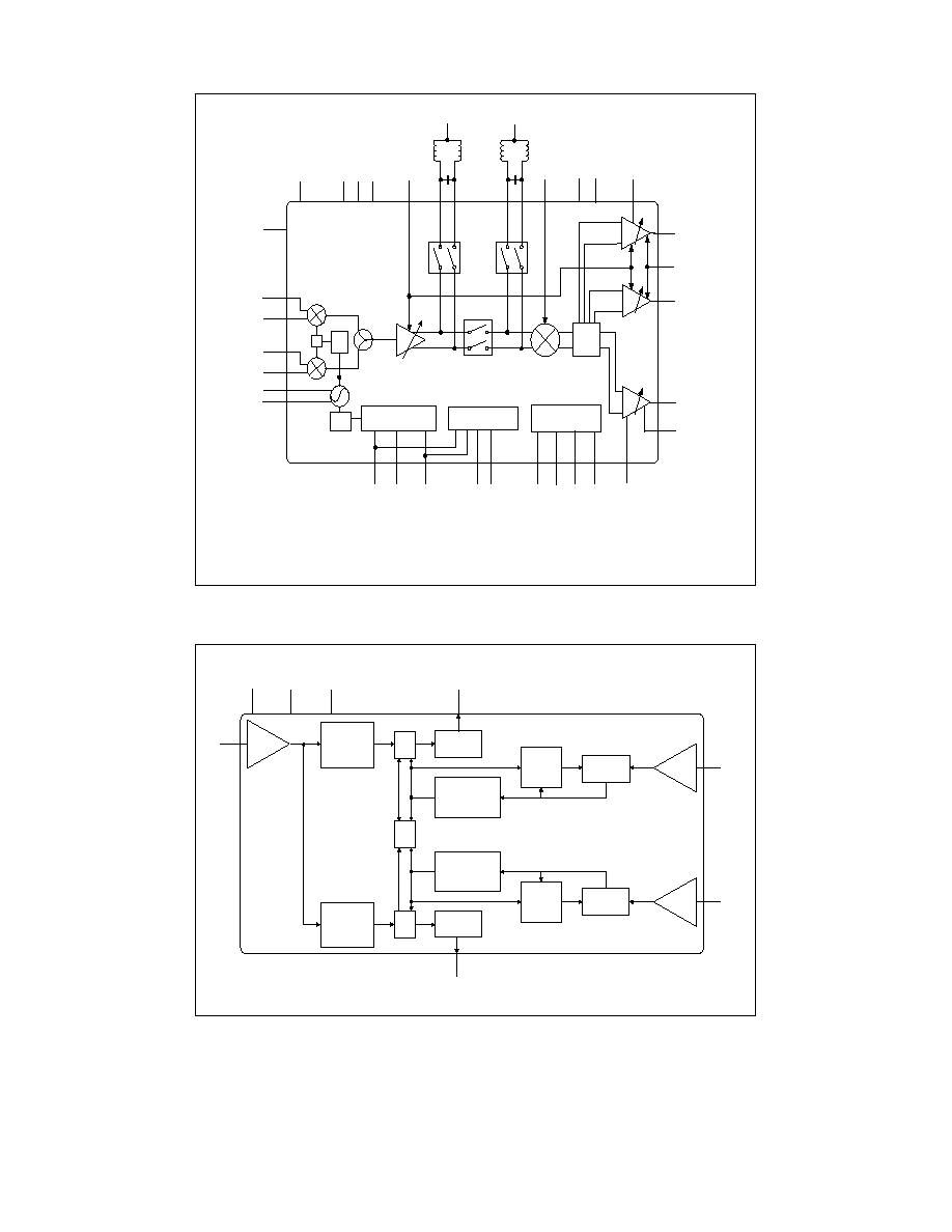
Figure 1. CX74002 Pinout 40-Pin LGA Package (Top View)
The CX74002 device is a single-supply, monolithic integrated
circuit. It is designed for use in dual-mode and multi-band
CDMA/AMPS/PCS cellular voice/data applications including
extensions for Japanese (CDMA-Japan) and Korea (PCS-
Korea).
The CX74002 is a highly integrated superheterodyne
transmitter that incorporates the following components:
·
·
·
·
·
In-Phase and Quadrature (I/Q) modulator accepts the
analog I and Q current outputs from the baseband analog
processor and converts them to Intermediate Frequency (IF)
signals
Voltage Controlled Oscillator (VCO) and VHF synthesizer
generates the LO signal for the quadrature modulators for
the cellular and the PCS bands
UHF synthesizer controls the UHF oscillator
Variable Gain Amplifier (VGA) provides the variable output
power for CDMA systems
Image reject upconverter and power amplifier (PA) drivers
The signal enters the chip as a baseband I/Q signal, which is
upconverted by an I/Q Quadrature Modulator. The resulting
signal is fed through a VGA to provide variable output power.
After leaving the open collector output of the VGA, the signal
enters a switch matrix. This switch matrix allows the signal to
be routed through an external filter, or it can be filtered by the
collector load and passed directly to the UHF image reject
mixer. This feature allows for dual Tx IF frequencies without
any external switching components. The image reject mixer is
internally connected to the PA driver. The mixer driver
combination has a variable gain control, which can be used to
reduce the RF gain, which improves the in-band Signal-to-
Noise Ratio (SNR) at a lower output power. The PA driver
amplifies the RF signal to the appropriate level for the desired
output power. This is then filtered by a bandpass filter and sent
to an external PA to obtain the final rated output power at the
antenna.
Skyworks Solutions, Inc., Proprietary and Confidential
1
101253B
[978] 241-7000 I FAX [978] 241-7906 I SALES@SKYWORKSINC.COM I WWW.SKYWORKSINC.COM
JANUARY 31, 2003
Data Sheet I CX74002
UHF
_
L
O
VC
C
B
i
a
s
VC
C
_
I
F
VCC_ IQ_MOD
C
D
M
A
D
r
i
v
er
Bi
as
VG
A_CT
RL
CDMA_DRV_OUT
PCS_DRV_O UT_B
PCS_DRV_O UT_A
IREF
PC
S
D
r
i
v
e
r
B
i
a
s
I+
I-
Q+
Q
VCO_T ANK+
Mux
Control Sig
VHF PLL
REF
VH
F
_
C
P
Lo
c
k
De
t
e
c
t
UHF PLL
UH
F
_
C
P
V
C
C_
CL
K
÷2
÷4
VC
C
VC
C
Enabl
e
DATA
CLK
TX
_
P
UNC
TURE
V
C
C_MIXER_1
V
C
C_MIXER_2
101253_002
÷2, 1
SYN_LO
POT_CELL
POT_PCS
VCO_T ANK
Figure 2. CX74002 Tx ASIC Block Diagram
VCC
_
V
H
F
VCC
_
U
H
F
UH
F_
C
P
REF
MUX
13-BIT
REFERENCE
COUNTER
PFD2
CHARGE
PUMP 2
12-BIT
PROGRAMMABLE
COUNTER
13-BIT
PROGRAMMABLE
COUNTER
13-BIT
REFERENCE
COUNTER
PFD1
CHARGE
PUMP 1
REF.
BUFFER
BUFFER
64/65
PRESCALER
8/9
PRESCALER
BUFFER
6-BIT
SWALLOW
COUNTER
3-BIT
SWALLOW
COUNTER
IF
UHF_LO
VHF_
C
P
V
C
C_
CL
K
101253_003
Figure 3. UHF/VHF PLL Block Diagram
2
Skyworks Solutions, Inc., Proprietary and Confidential
JANUARY 31, 2003
[978] 241-7000 I FAX [978] 241-7906 I SALES@SKYWORKSINC.COM I WWW.SKYWORKSINC.COM
101253B
Data Sheet I CX74002
Skyworks Solutions, Inc., Proprietary and Confidential
3
101253B
[978] 241-7000 I FAX [978] 241-7906 I SALES@SKYWORKSINC.COM I WWW.SKYWORKSINC.COM
JANUARY 31, 2003
Technical Description
A
C
B
VGA_OUT
IF_IN
VGA
MIXER
I/Q Modulator and VGA
The I/Q modulator converts the incoming I/Q signal to an IF
signal, then feeds it directly to the VGA. The LO for the I/Q
modulator is generated by the VHF VCO and is controlled by the
VHF PLL. The I/Q modulator has two input modes: voltage
mode and current mode. The voltage mode operates with
1.0 Vp-p differential I/Q inputs. In the current mode, a DC input
current of 1.0 mA is required with ±0.5 mA signal swing. The
modulator supports direct I/Q or direct VCO modulation in the
AMPS mode. The VGA has 90 dB of dynamic range. The open
collector output requires an inductor pull-up to VCC and filtered
to reject noise that falls in the receiver band.
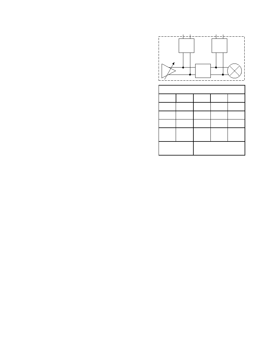
Switch Modes
IFout1 IFout2 A
B
C
0 0 1 0 1
0 1 1 1 0
1 0 0 1 1
1 1
Not
used
Not
used
Not
used
0 = Logic low
1= Logic high
0 = Open
1 = Closed
VHF, VCO, and PLL
The VHF VCO has a frequency range of 200 to 700 MHz and
requires an external tank circuit. This tank circuit can be used
to provide the analog FM modulation in the AMPS mode. The
VHF VCO is connected to an on-chip VHF PLL. The frequency of
the VCO output is divided by 2 or 4 to derive the I/Q LO signals
for the I/Q modulator. Also, an additional divide by 2/4 is
derived from the tank frequency before input to the VHF PLL
buffer.
The VHF loop of the synthesizer has a 16-bit N divider and a
13-bit R divider (see Figure 3). The charge pump has four
programmable discreet levels from 100 to 400 µA. The VHF
PLL is supplied by the VCC_DIV and VCC_VHF pins, and the
VCO output follows an internal path to the I/Q modulator. As a
result, the VHF PLL must be used for proper operation of the
device. However, the VHF PLL and the VHF VCO may be
enabled and disabled independently through the serial bus.
Figure 4. VGA/Upconverter Switching Diagram
1100 MHz for the cellular band and 1600 to 2200 MHz for the
PCS band). The upconverter can be programmed for high side
(RF = LO IF) or low side (RF = LO + IF) operation. Using an
image reject mixer eliminates the need for an image reject
SAW filter.
The output of the mixer may be routed to either the CDMA PA
driver or the PCS PA driver. At a low output power level, RF
gain is reduced to improve the SNR of the signal. The variable
gain function is controlled by VGA_CTRL signal, which also
controls IF VGA.
Switch Matrix
To provide the maximum flexibility for multiple IF frequency
plans, there is a switch matrix between the VGA output and the
upconverter input. This switch matrix allows a direct
connection between the VGA and the upconverter and provides
two external ports for the VGA's open collector output. An LC
tank circuit can be used as the open collector load at the
VGA_OUT pins or the IF_IN pins, or both. This load provides
adequate Rx band noise filtering without an expensive external
SAW filter.
Synthesizer
A dual UHF/VHF synthesizer has been integrated into the
CX74002. This dual, multi-band frequency synthesizer has fully
programmable dividers and selected charge pump currents for
on-chip VHF VCO and external UHF VCO operation.
The UHF synthesizer operates from 600 to 2200 MHz. It takes
its reference signal from the REF pin. The programming of the
UHF synthesizer is provided through the serial bus (see
Figure 3). This synthesizer includes a 13-bit R divider and an
18-bit N divider. The charge pump current is adjustable and
has four discrete steps between 0.8 mA and 2.7 mA. The UHF
PLL has an independent power supply from the rest of the
device. As a result, the UHF PLL can remain operational when
the remainder of the CX74002 is disabled. The Rx LO can be
also supplied from the same synthesizer, minimizing the total
component count and minimizing the total current when only
the Rx portion of the radio is in operation. If an external PLL is
desired, the UHF PLL can be disabled without adversely
affecting the operation of the CX74002.
Dual Tx IF frequencies plan (single Rx IF [SIF] frequency plan)
can be easily implemented by using two separate LC tank
circuits on the VGA_OUT pin and the IF_IN pin: one set is tuned
to the cellular band, the other set is tuned to the PCS band. An
external dual-port filter can also be used between the
VGA_OUT pin and IF_IN pin for IF filtering before the signal
goes into the upconverter. The operation of this switch matrix
is programmed by using the serial bus interface (see Figure 4).
Variable RF Gain Image Reject Upconverter
The image reject upconverter receives the IF signal from the Tx
VGA after passing through the switch matrix. The upconverter
uses an external UHF VCO, controlled by the internal UHF PLL.
The UHF LO frequency can vary from 600 to 2.2 GHz (600 to

Data Sheet I CX74002
PA Drivers
Three PA drivers are included: the CDMA driver and two PCS
drivers. Each driver takes its input from the image reject
upconverter. The driver amplifies the signal and sends it to an
external PA. A SAW filter for noise rejection should be used
between the driver and the external PA. The primary purpose
of the SAW is to reduce the Rx band noise from the signal
this Rx band noise can leak through the duplexer and reduce
the sensitivity of the receiver. Two outputs are provided in the
PCS band to facilitate the use of a split band filter at the PCS
output.
Serial Bus
A 3-wire serial bus is provided for mode control. The serial bus
is also used to program both the VHF and the UHF PLLs.
Electrical and Mechanical Specifications
Signal pin assignments and functional pin descriptions are
described in Table 1. The absolute maximum ratings of the
CX74002 are provided in Table 2. The recommended operating
conditions are specified in Table 3 and electrical specifications
are provided in Table 4. Tables 5 through 12 provide the
control logic and timing for the CX74002. Timing diagrams are
shown in Figures 5 and 6 for the synthesizer and serial data
word, respectively.
Typical performance characteristics of the CX74002 are
illustrated in Figures 7 through 28. Figure 29 shows an
application schematic diagram. The package dimensions for
the CX74002 40-pin RFLGA are shown in Figure 30, and the
tape and reel dimensions are provided in Figure 31.
Electrostatic Discharge (ESD) Sensitivity
The CX74002 is a static-sensitive electronic device. Do not
operate or store near strong electrostatic fields. Take proper
ESD precautions. The Human Body Model (HBM) ESD
withstand threshold value, with respect to ground, is
±1.5 kV.
The HBM ESD withstand threshold value, with respect to VCC
(the positive power supply terminal), is also 1.5 kV.
4
Skyworks Solutions, Inc., Proprietary and Confidential
JANUARY 31, 2003
[978] 241-7000 I FAX [978] 241-7906 I SALES@SKYWORKSINC.COM I WWW.SKYWORKSINC.COM
101253B
Data Sheet I CX74002
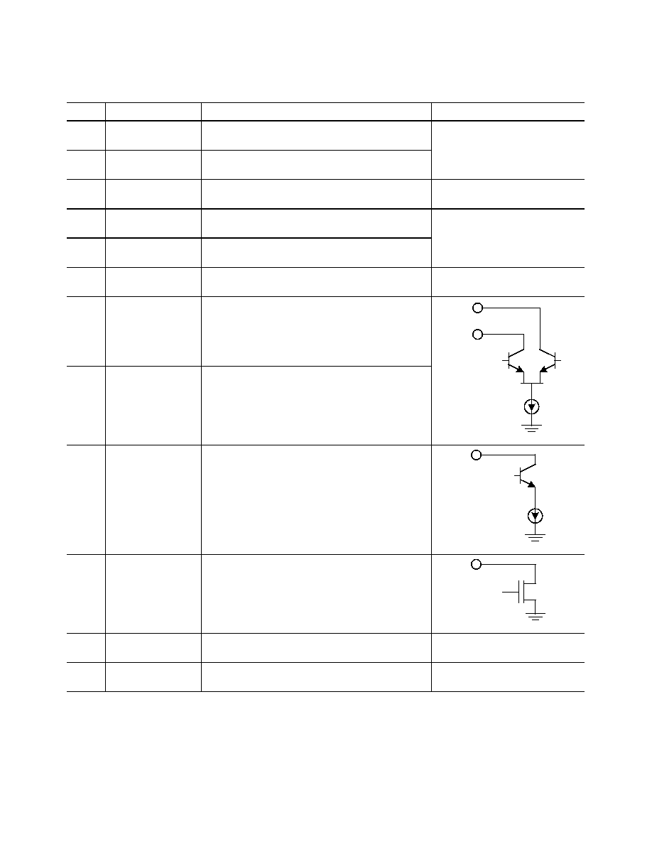
Table 1. CX74002 Pin Assignments and Signal Descriptions (1 of 3)
Pin #
Name
Description
Equivalent Circuit
1
VCC_IF
VCC for the IF VGA and the mixer input buffer
2
Q+
Q+ input. High input impedance for voltage mode; low input
impedance for current mode.
3
Q
Q input. High input impedance for voltage mode; low input
impedance for current mode.
4
VCC_IQ_MOD
VCC for the I/Q modulator. Also shared by divide-by-2/4 last
stage, all the bias blocks (Note 1).
5
I+
I+ input. High input impedance for voltage mode; low input
impedance for current mode.
6
I
I input. High input impedance for voltage mode; low input
impedance for current mode.
7
VCC_DIV
VCC for the bias circuit of the VCO, VHF PLL buffer, divide-by-
2/4 first stage (Note 2).
8 VCO_TANK+
VCO
tank
9 VCO_TANK
VCO
tank
+
10
IREF
Output to the baseband chip during the current I/Q mode.
This pin is not used and left open during the voltage I/Q
mode.
11
POT_IREF
External resistor (120 k typical) is required to set the current
in the PLLs and the IREF.
12
VCC_CLK
VCC supplies the TCXO buffers and related circuitry. Should
be kept separate from analog supply (Note 1) (Note 2).
13
VCC_VHF
VCC for the VHF Prescalar, VHF, UHF counters, and the serial
bus (Note 1) (Note 2).
Skyworks Solutions, Inc., Proprietary and Confidential
5
101253B
[978] 241-7000 I FAX [978] 241-7906 I SALES@SKYWORKSINC.COM I WWW.SKYWORKSINC.COM
JANUARY 31, 2003
Document Outline