101787a.book
Data Sheet
101787A
© 2001, 2002 Skyworks Solutions, Inc., All Rights Reserved.
December 10, 2002
CX77105
Power Amplifier Module for CDMA/AMPS (824849 MHz)
The CX77105, a dual-mode, Code Division Multiple Access (CDMA) / Advanced
Mobile Phone Service (AMPS) Power Amplifier Module (PAM), is a fully matched,
10-pin surface mount module developed for cellular handsets and wireless local loop
applications. This small and efficient power amplifier module packs a full 824849
MHz bandwidth coverage into a single compact package. The device meets the
stringent IS95 CDMA linearity requirements to and exceeding 28 dBm output power,
and can be driven to levels beyond 31 dBm for high efficiency in FM mode operation.
A low current digital pin (VCONT) provides improved efficiency for the low RF power
range of operation.
The single Gallium Arsenide (GaAs) Microwave Monolithic Integrated Circuit (MMIC)
contains all active circuitry in the module. The MMIC contains on-board bias circuitry,
as well as input and interstage matching circuits. The output match is realized off-chip
and within the module package to optimize efficiency and power performance into a
50
load. This device is manufactured with Skyworks' GaAs Heterojunction Bipolar
Transistor (HBT) process that provides for all positive voltage DC supply operation
while maintaining high efficiency and good linearity. Primary bias to the CX77105 is
supplied directly from a three-cell nickel cadmium, a single-cell lithium ion, or other
suitable battery with an output in the 34 volt range. Power down is accomplished by
setting the voltage on the low current reference pin to zero volts. No external supply
side switch is needed as typical "off" leakage is a few microamperes with full primary
voltage supplied from the battery.
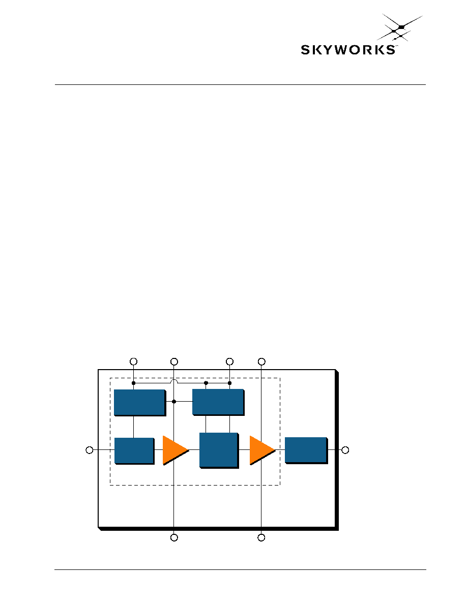
Functional Block Diagram
MMIC
MODULE
RF IN (4)
(8) RF OUT
VCC1
(3, 7, 9, 10)
GND
(3, 7, 9, 10)
GND
VCC2
VREF
Driver
Driver
Stage Bias
Stage Bias
Power
Power
Stage Bias
Stage Bias
Input
Input
Match
Match
DA
DA
Inter
Inter
Stage
Stage
Match
Match
PA
PA
Output
Output
Match
Match
(1)
(5)
(6)
VCONT
(2)
Distinguishing Features
·
Low voltage positive bias supply
(3.2 V to 4.2 V, typical)
·
Good linearity
·
High efficiency
·
Dual mode operation
·
Large dynamic range
·
10-pin package (4 x 4 x 1.5 mm)
·
Power down control
·
Low power-state control
·
InGaP
·
IS 95/CDMA2000
Applications
·
Digital cellular (CDMA)
·
Analog cellular (AMPS)
·
Wireless local loop (WLL)
Electrical Specifications
CX77105
Power Amplifier Module for CDMA/AMPS (824849 MHz)
2
Skyworks Solutions, Inc. Proprietary
101787A
December 10, 2002
Electrical Specifications
The following tables list the electrical characteristics of the CX77105 Power Amplifier.
Table 2
lists the recommended operating conditions for achieving the electrical performance listed in
Table 4
.
Table 3
lists the electrical performance of the CX77105 Power Amplifier over the
recommended operating conditions.
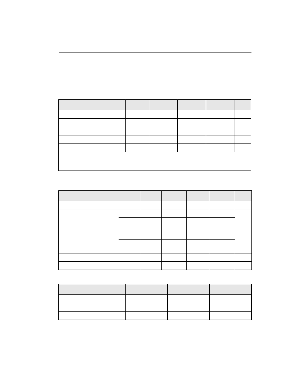
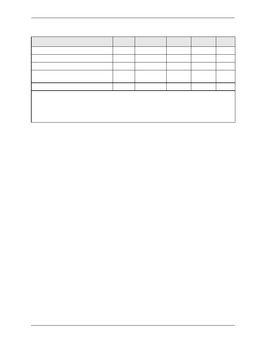
Table 1. Absolute Maximum Ratings
(1)
Parameter
Symbol
Minimum
Nominal
Maximum
Unit
RF Input Power
P
IN
--
4.0
7.0
dBm
Supply Voltage
V
CC
--
3.4
6.0
Volts
Reference Voltage
V
REF
--
3.0
3.1
Volts
Case Operating Temperature
T
C
30
25
+110
o
C
Storage Temperature
T
STG
55
--
+125
o
C
NOTE(S):
(1)
No damage assuming only one parameter is set at limit at a time with all other parameters set at or below
nominal value.
Table 2. Recommended Operating Conditions
Parameter
Symbol
Minimum
Nominal
Maximum
Unit
Supply Voltage
V
CC
3.2
3.4
4.2
Volts
Reference Voltage
PA On
V
REF
2.95
3.0
3.05
Volts
PA Off
V
REF
--
--
0.5
Mode Input Impedance >2.5 k
High
Bias
V
CONT
0.0
--
0.5
Volts
Low
Bias
V
CONT
2.5
--
3.0
Operating Frequency
F
O
824.0
836.5
849.0
MHz
Operating Temperature
T
O
30 -- +85 °C
Table 3. Power Range Truth Table
Power Mode
VREF
VCONT
Range
High Power
3.0 V
0.00.5 V
16 dBm28 dBm
Low Power
3.0 V
2.53.0 V
16 dBm
Shut Down
0.0 V
0.0 V
--
CX77105
Electrical Specifications
Power Amplifier Module for CDMA/AMPS (824849 MHz)
101787A
Skyworks Solutions, Inc. Proprietary
3
December 10, 2002
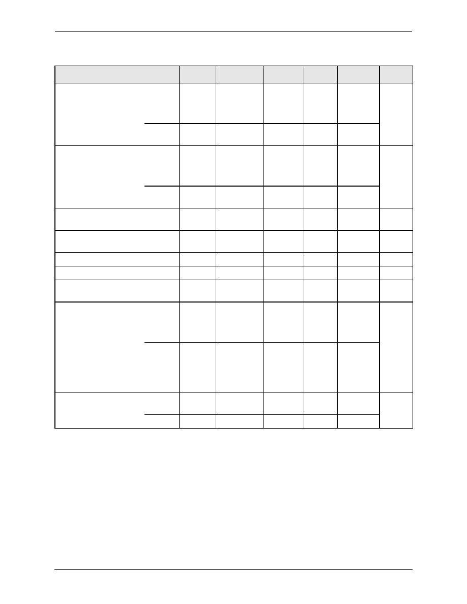
Table 4. Electrical Specifications for CDMA / AMPS Nominal Operating Conditions
(1)
Characteristics
Symbol
Condition
Minimum
Typical
Maximum
Unit
Gain conditions
Digital
Mode
G
LOW
G
HIGH
V
CONT
2.5 V
P
O
= 16 dBm
V
CONT
0.5 V
P
O
= 28 dBm
25.0
28.5
27.0
29.0
28.0
31.0
dB
Analog
Mode
G
P
V
CONT
0.5 V
P
O
= 31 dBm
27.5
29.0
31.0
Power Added Efficiency
Digital
Mode
PAE
LOW
PAE
HIGH
V
CONT
2.5 V
P
O
= 16 dBm
V
CONT
0.5 V
P
O
= 28 dBm
7.6
37.0
8.5
40.0
--
--
%
Analog
Mode
PAEa
V
CONT
0.5 V
P
O
= 31 dBm
48.0
55.0
--
Total Supply Current
I
CC_LOW
I
CC_HIGH
P
O
= 16 dBm
P
O
= 28 dBm
--
--
137
490
153
500
mA
Quiescent Current
I
Q_LOW
I
Q_HIGH
V
CONT
2.5 V
V
CONT
0.5 V
40
60
55
78
75
105
mA
Reference Current
I
REF
--
--
2.5
5.0
mA
Control Current
I
CTRL
V
CONT
= 2.5 V
200
235
500
µA
Total Supply current in Power-down
Mode
I
PD
V
CC
= 3.4 V
V
REF
= 0 V
--
3.0
5.0
µA
Adjacent Channel
Power
(2)(3)
885 kHz
offset
ACP1
LOW
ACP1
HIGH
V
CONT
2.5 V
P
O
16 dBm
V
CONT
0.5 V
P
O
28 dBm
--
--
49.0
50.0
47.3
47.0
dBc
1.98
MHz
offset
ACP2
LOW
ACP2
HIGH
V
CONT
2.5 V
P
O
16 dBm
or
V
CONT
0.5 V
P
O
28 dBm
--
--
65.0
60.0
59.0
57.4
Harmonic Suppression
Secon
d
F
O
2
P
O
28 dBm
--
38.0
35.0
dBc
Third
F
O
3
P
O
28 dBm
--
59.0
45.0
Electrical Specifications
CX77105
Power Amplifier Module for CDMA/AMPS (824849 MHz)
4
Skyworks Solutions, Inc. Proprietary
101787A
December 10, 2002
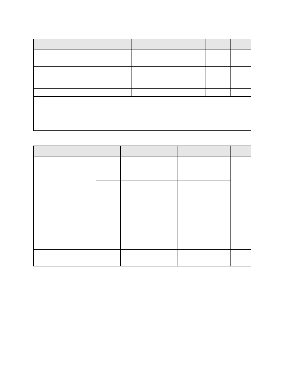
Noise Power in RX Band 869-894 MHz
RxBN
P
O
28 dBm
--
137
--
dBm/Hz
Noise Figure
NF
--
--
4.6
5.0
dB
Input Voltage Standing Wave Ratio
VSWR
--
--
--
1.9:1
--
Stability (Spurious output)
S
5:1 VSWR
all phases
--
--
60.0
dBc
Ruggedness--No damage
(4)
Ru
P
O
28 dBm
10:1
--
--
VSWR
NOTE(S):
(1)
V
CC
= +3.4 V, V
REF
= +3.0 V, Freq = 836.5 MHz, T
C
= 25 °C, unless otherwise specified.
(2)
ACP is specified per IS95 as the ratio of the total in-band power (1.23 MHz BW) to adjacent power in a 30 kHz BW.
(3)
CDMA2000 is configured as DCCH = 9600, SCHO = 9600, PCH (Walsh 0) = 3.75 dB, and Peak-to-Average Ratio
(CCDF = 1%) = 4.5 dB. For CDMA2000, 0.5 dB back-off in output power is required.
(4)
All phases, time = 10 seconds.
Table 4. Electrical Specifications for CDMA / AMPS Nominal Operating Conditions
(1)
Characteristics
Symbol
Condition
Minimum
Typical
Maximum
Unit
Table 5. Electrical Specifications for CDMA / AMPS Recommended Operating Conditions
(1)
Characteristics
Symbol
Condition
Minimum
Maximum
Unit
Gain conditions
Digital
Mode
G
LOW
G
HIGH
V
CONT
2.5 V
P
O
= 16 dBm
V
CONT
0.5 V
P
O
= 28 dBm
24.0
27.1
28.5
32.4
dB
Analog
Mode
G
P
V
CONT
0.5 V
P
O
= 31 dBm
24.0
33.0
Adjacent Channel Power
(2)(3)
1.25 MHz
offset
ACP1
LOW
ACP1
HIGH
V
CONT
2.5 V
P
O
16 dBm
V
CONT
0.5 V
P
O
28 dBm
--
--
44
44
dBc
dBc
1.98 MHz
offset
ACP2
LOW
ACP2
HIGH
V
CONT
2.5 V
P
O
16 dBm
or
V
CONT
0.5 V
P
O
28 dBm
--
--
56
56
dBc
dBc
Harmonic Suppression
Second
F
O
2
P
O
28 dBm
--
30
dBc
Third
F
O
3
P
O
28 dBm
--
40
dBc
CX77105
Electrical Specifications
Power Amplifier Module for CDMA/AMPS (824849 MHz)
101787A
Skyworks Solutions, Inc. Proprietary
5
December 10, 2002
Noise Power in RX Band 869-894 MHz
RxBN
P
O
28 dBm
--
134.0
dBm/Hz
Noise Figure
NF
--
--
7.0
dB
Input Voltage Standing Wave Ratio (VSWR)
VSWR
--
--
2.0:1
--
Stability (Spurious output)
S
5:1 VSWR
All phases
--
60.0
dBc
Ruggedness No damage
(4)
Ru
P
O
28dBm
10:1
--
VSWR
NOTE(S):
(1)
Per Table 2, unless otherwise specified.
(2)
ACP is specified per IS95 as the ratio of the total in-band power (1.23 MHz BW) to adjacent power in a 30 kHz BW.
(3)
CDMA2000 is configured as DCCH = 9600, SCHO = 9600, PCH (Walsh 0) = 3.75 dB, and Peak-to-Average Ratio
(CCDF = 1%) = 4.5 dB. For CDMA2000, 0.5 dB back-off in output power is required.
(4)
All phases, time = 10 seconds.
Table 5. Electrical Specifications for CDMA / AMPS Recommended Operating Conditions
(1)
Characteristics
Symbol
Condition
Minimum
Maximum
Unit
Document Outline