
Data Sheet
Preliminary Information
101537P6
© 2001, 2002 Skyworks Solutions, Inc., All Rights Reserved.
March 27, 2002
Preliminary Information
This document contains information on a new product. The parametric information, although not
fully characterized, is the result of testing initial devices.
CX77133
Power Amplifier Module for CDMA PCS (1850≠1910 MHz)
The CX77133 Power Amplifier Module (PAM) is a fully matched, 6-pin surface mount
module developed for Personal Communications Service (PCS) and wireless local
loop applications. This small and efficient Power Amplifier packs a full 1850≠1910
MHz bandwidth coverage into a single compact package.
The CX77133 meets the stringent spectral linearity requirements of Code Division
Multiple Access (CDMA) PCS transmission with high power added efficiency for
power output of up to 28 dBm. A single Gallium Arsenide (GaAs) Microwave
Monolithic Integrated Circuit (MMIC) contains all the active circuitry in the module.
The MMIC contains on-board bias circuitry, as well as input and interstage matching
circuits. Output match is realized off-chip within the module package to optimize
efficiency and power performance into a 50
load.
This device is manufactured with Skyworks' GaAs Heterojunction Bipolar Transistor
(HBT) process, which provides for all positive voltage DC supply operation while
maintaining high efficiency and good linearity. Primary bias to the CX77133 is
supplied directly from a three-cell nickel cadmium, a single-cell lithium ion, or other
suitable battery with an output in the 3≠4 volt range. Power down is accomplished by
setting the voltage on the low current reference pin to zero volts. No external supply
side switch is needed as typical "off" leakage is a few microamperes with full primary
voltage supplied from the battery.
Functional Block Diagram
MMIC
MODULE
RF
Output
(5)
RF
Input
(2)
VCC1
(1)
(6, 7)
GND
VCC2
(4)
VREF
(3)
Driver
Stage Bias
Power
Stage Bias
Input
Match
DA
Inter
Stage
Match
PA
Output
Match
(6, 7)
GND
Distinguishing Features
∑
Low voltage positive bias supply
(3 to 4 Volts)
∑
Good linearity
∑
High efficiency
∑
Large dynamic range
∑
6-pin package (6 x 6 x 1.5 mm)
∑
Power down control
Applications
∑
Personal communications
services (PCS)
∑
Wireless local loop (WLL)

Electrical Specifications
CX77133
Power Amplifier Module for CDMA PCS (1850≠1910 MHz)
2
Skyworks
101537P6
Preliminary Information
March 27, 2002
Electrical Specifications
The following tables list the electrical characteristics of the CX77133 Power Amplifier.
Table 1
lists the absolute maximum rating for continuous operation.
Table 2
lists the recommended operating conditions and
Table 3
lists the electrical performance of
the CX77133 Power Amplifier for nominal operating conditions.
Table 1. Absolute Maximum Ratings
(1)
Parameter
Symbol
Minimum
Nominal
Maximum
Unit
RF Input Power
P
IN
--
4.0
7.0
dBm
Supply Voltage
V
CC
--
3.4
6.0
Volts
Reference Voltage
V
REF
--
3.0
3.3
Volts
Case Operating Temperature
T
C
≠30
+25
+110
o
C
Storage Temperature
T
STG
≠55
--
+125
o
C
NOTE(S):
(1)
No damage assuming only one parameter is set at limit at a time with all other parameters set at or below
nominal value.
Table 2. Recommended Operating Conditions
Parameter
Symbol
Min
Nominal
Max
Unit
Supply Voltage
V
CC
3.2
3.4
4.2
Volts
Reference Voltage
V
REF
2.95
3.0
3.2
Volts
Operating Frequency
F
O
1850.0
1880.0
1910.0
MHz
Case Operating Temperature
T
C
≠30
+25
+85
∞C

CX77133
Electrical Specifications
Power Amplifier Module for CDMA PCS (1850≠1910 MHz)
101537P6
Skyworks
3
March 27, 2002
Preliminary Information
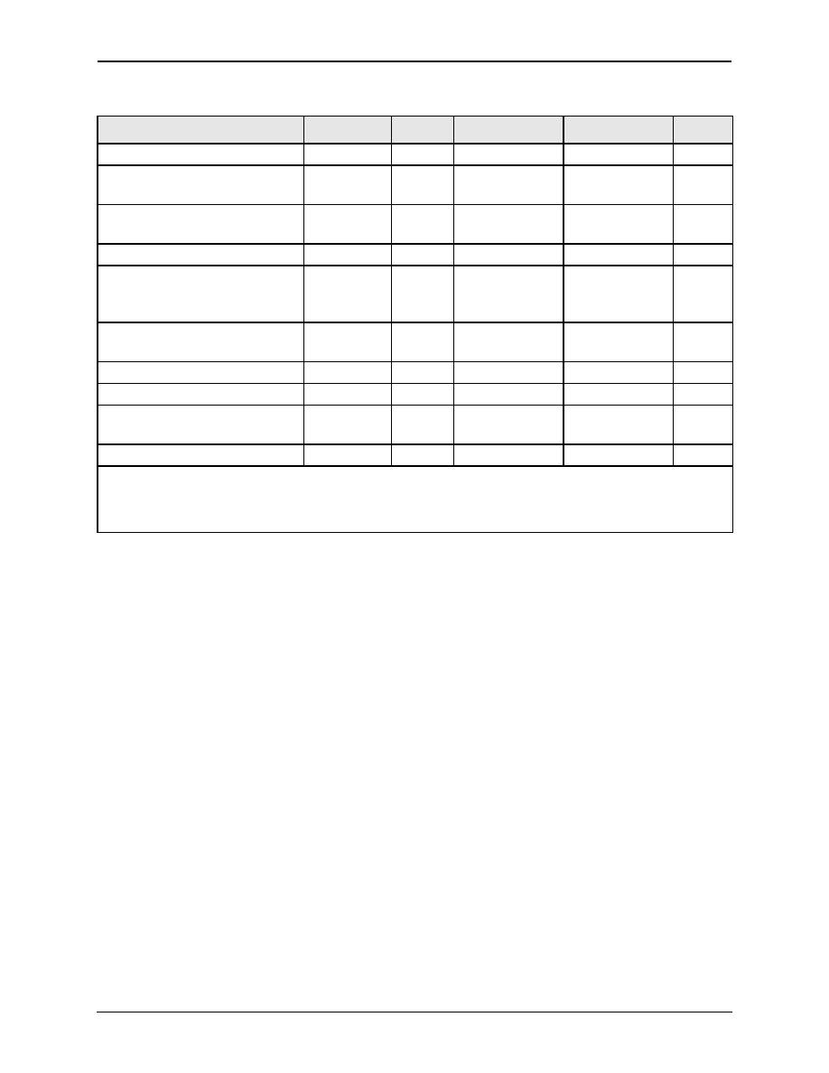
Table 3. Electrical Specification for Nominal Operating Conditions
(1)
Characteristics
Condition
Symbol
Minimum
Typical
Maximum
Unit
Quiescent Current
Nominal
I
q
70.0
120.0
130.0
mA
Leakage Current
V
REF
= 0 V
V
CC
= 3.4 V
I
lk
--
--
7.0
µA
Gain
P
O
= 0 dBm
P
O
= 28 dBm
G
G
p
25.5
27.0
26.5
28.5
28.0
30.0
dB
dB
Power Added Efficiency
P
O
= 28 dBm
PAEd 28
32.0
36.0
--
%
Adjacent Channel Power
P
O
28 dBm
(2)
ACP
--
≠50.0
≠48.5
dBc
Harmonic Suppression
Second
Third
P
O
28 dBm
P
O
28 dBm
DF
O
2
DF
O
3
--
--
≠38.0
≠44.0
≠32.0
≠37.5
dBc
dBc
Noise Power in RX Band
1930-1990 MHz
P
O
28 dBm
R
X
BN
--
≠135.0
≠133.0
dBm/Hz
Noise Figure
--
NF
--
4.0
5.5
dB
Input Voltage Standing Wave Ratio
--
VSWR
--
1.2
1.4
--
Stability (spurious output)
5:1 VSWR
All Phases
S
--
--
≠60.0
dBc
Ruggedness ≠ No damage
P
O
28 dBm
Ru
10:1
--
--
VSWR
NOTE(S):
(1)
V
CC
= +3.4 V, V
REF
= +3.0 V, Freq. = 1880 MHz, T
C
= 25
o
C, unless otherwise specified.
(2)
ACP is specified per IS95 as the ratio of the total in-band power (1.23 MHz BW) to adjacent power in a 30 kHz BW
Electrical Specifications
CX77133
Power Amplifier Module for CDMA PCS (1850≠1910 MHz)
4
Skyworks
101537P6
Preliminary Information
March 27, 2002
Table 4. Electrical Specification Limits for Recommended Operating Conditions
(1)
Characteristics
Condition
Symbol
Minimum
Maximum
Unit
Quiescent Current
Nominal
I
q
--
180.0
mA
Gain
P
O
= 0 dBm
P
O
= 28 dBm
G
G
p
24.0
23.0
29.5
32.5
dB
dB
Power Added Efficiency
V
CC
= 3.4 V
P
O
= 28 dBm
PAEd 28
31.5
--
%
Adjacent Channel Power
(2)
P
O
28 dBm
ACP
--
≠44.0
dBc
Harmonic Suppression
Second
Third
P
O
28 dBm
P
O
28 dBm
DF
O
2
DF
O
3
--
≠30.0
≠35.0
dBc
dBc
Noise Power in RX Band
1930-1990 MHz
P
O
28 dBm
R
X
BN
--
≠131.0
dBm/Hz
Noise Figure
--
NF
--
8.0
dB
Input Voltage Standing Wave Ratio
--
VSWR
--
2.0
--
Stability (spurious output)
5:1 VSWR
All Phases
S
--
≠60.0
dBc
Ruggedness≠No damage
P
O
28 dBm
Ru
10:1
--
VSWR
NOTE(S):
(1)
Per Table 2, unless otherwise specified.
(2)
ACP is specified per IS95 as the ratio of the total in-band power (1.23 MHz BW) to adjacent power in a 30 kHz BW.
Worst case ACPR is ≠43dBc at +85 ∞C, Vcc = 3.2 V.

CX77133
Evaluation Board Description
Power Amplifier Module for CDMA PCS (1850≠1910 MHz)
101537P6
Skyworks
5
March 27, 2002
Preliminary Information
Evaluation Board Description
The evaluation board is a platform for testing and interfacing design circuitry. To accommodate the
interface testing of the CX77133, the evaluation board schematic and diagrams are included for
preliminary analysis and design.
Figure 1
shows the basic schematic of the board for the
1850 MHz to 1910 MHz range.
Figure 2
illustrates the board layout.
Figure 1. Evaluation Board Schematic
Figure 2. Evaluation Board Assembly Diagram
101537_003
1
2
3
6
5
4
VCC1
RFIN
RFIN
VREF
VREF
GND
RFOUT
RFOUT
VCC2
VCC
C3
330 pF
C4
1000 pF
C1
220 pF
C2
4.7 µF
101537_002
Vref
GND
GND
Vcc
C2
C4
C3
C1
RF OUT
RF IN
SKYWORKS
6x6_ENG_EVAL_BD