 | –≠–ª–µ–∫—Ç—Ä–æ–Ω–Ω—ã–π –∫–æ–º–ø–æ–Ω–µ–Ω—Ç: RF25L | –°–∫–∞—á–∞—Ç—å:  PDF PDF  ZIP ZIP |

Data Sheet
Skyworks ≠ Preliminary
Doc. No. 101174B
Proprietary Information and Specifications are Subject to Change
January 14, 2002
RF25L
Tx ASIC for CDMA, AMPS, and PCS Applications
The RF25L includes the following functional blocks:
∑
In-Phase and Quadrature (I/Q) modulator
∑
Very High Frequency (VHF) Voltage Controlled Oscillator (VCO)
∑
Intermediate Frequency (IF) Variable Gain Amplifier (VGA)
∑
Cellular and Personal Communications System (PCS) upconverters with RF
gain control
∑
Cellular and PCS Power Amplifier (PA) drivers
The RF25L Application-Specific Integrated Circuit (ASIC) is a triple-mode, dual-
band transmitter intended for use in Code Division Multiple Access (CDMA) phones
in both cellular and PCS bands. As a dual mode IC, it can be used in either CDMA
mode or Advanced Mobile Phone System (AMPS) mode.
The RF25L incorporates all the components to implement the completed
transmitter chain; from the I/Q modulator to the PA driver amplifier, except for
external IF and RF SAW filters. The I/Q modulator receives differential inputs from
the baseband and upconverts to IF band. The on-chip VHF VCO operates with an
external tank circuit to provide the Local Oscillator (LO) signal for the I/Q
modulator. The VGA amplifies the IF signal with a minimum dynamic range of 90
dB. After external IF filtering, the signal is upconverted to RF frequency in either
Cellular or PCS mode depending on the band selected control pin. Both the cellular
and PCS mixers have an adjusted variable gain option to compensate for gain
variation of off-chip components. The RF signal is filtered through an external filter
and inputs to the drive amplifier.
The Gain, ACPR and Noise Figure of each stage in the RF25L are optimized to
meet the system requirements per TIA/EIA-98-B and ANSI J-STD-018. The chip is
designed for cost-effective performance with high level integration in silicon bipolar
technology.
The device package and pinout are shown in Figure 1. A block diagram of the
RF25L is shown in Figure 2.
Features
∑
Supports dual-band, tri-mode operation
∑
90 dB dynamic range
∑
On-chip 100 to 640 MHz VCO
∑
Adjustable RF mixer gain option
∑
Lower power consumption
∑
Dual drivers for cellular and PCS bands
∑
48-Pin Land Grid Array (LGA), 7 x 7 mm package
Applications
∑
Tri-mode phones
∑
In cellular band:
-
AMPS
-
CDMA (US)
-
CDMA (Japan)
∑
In the PCS band:
-
PCS (US)
-
PCS (Korean)
CNXT025
NC
NC
PLL_M
PLL_P
NC
VCC_DIV
CELL_MIX_OUT
CHIP_ENABLE
VCC_DIFF_DRV
PCS_MIX_OUT
NC
NC
MIX_IN_M
MIX_IN_P
CELL_LO
VCC_MIX
PCS_LO
NC
V
G
A_GC
VCO_T
ANK_M
VCO_T
ANK_P
FM_CDMA_SELECT
NC
NC
NC
VCC_IF
RF_GC
VGA_OUT_P
VGA_OUT_M
VCC_PCS_LAST_DRV
CELL_POT
DRIVER_ON
PCS_DRV_OUT
VCC_BIAS
CELL_DRV_OUT
NC
NC
BAND_SELECT
VCC_CELL_DR
V
PCS_PO
T
VCC_PCS_MID
CELL_DR
V_IN
PCS_DR
V_IN
I_D
A
T
A_P
I_D
A
T
A_M
VCC_IQ_MOD
Q_D
A
T
A_P
Q_D
A
T
A_M
1
2
3
4
5
6
7
8
9
10
11
12
13
37
36
35
34
33
32
31
30
29
28
27
26
25
48
47
46
45
44
43
42
41
40
39
38
14
15
16
17
18
19
20
21
22
23
24
Figure 1. RF25L Tx ASIC Pinout
48-Pin LGA Package

RF25L
Tx ASIC for CDMA, AMPS, and PCS Applications
2
Skyworks ≠ Preliminary
101174B
Proprietary Information and Specifications are Subject to Change
January 14, 2002
CNXT027
VGA_GC
130.38 MHz
CELL_DRV_OUT
PCS_DRV_OUT
RF SAW (CELL)
RF SAW (PCS)
Control
Block
PCS_LO
BAND_SELECT
CHIP_ENABLE
TO VCO TANK
Q Data
Tx VGA
I Data
I
Q
˜2
TO PLL
RF_GC
Lo Buf
Lo Buf
DRIVER_ON
42
4
5
46
39
31
18
8
11
9
28
19
3
44
14
30
35
34
41
40
24
23
21
20
47
48
CELL_LO
FM_CDMA
SELECT
Figure 2. RF25L Tx ASIC Block Diagram

Tx ASIC for CDMA, AMPS, and PCS Applications
RF25L
101174B
Skyworks ≠ Preliminary
3
January 14, 2002
Proprietary Information and Specifications are Subject to Change
Technical Description
I/Q Modulator. The I/Q modulator upconverts the incoming
differential I & Q analog baseband signals to IF signals using the
VHF local oscillator. These signals are fed directly to the VGA.
VHF VCO. Works with an external tank circuit and a varactor
diode, which may operate from 100 to 640 MHz. The differential
output signals from the oscillator are buffered and used to drive
the prescalar of an external Phase Lock Loop (PLL). The VCO
typically operates at twice of the IF frequency.
VGA. The VGA has a minimum dynamic range of 90 dB with a
control voltage of 0.5 to 2.5 Volts.
Upconverters. The cellular and PCS upconverters convert the
Tx signal from the IF frequency to the PCS or cellular RF for
optimum phone performance. Upconverter conversion gain
control can be used to compensate part-to-part and temperature
gain variations in the transmit path. The band select command
switches between the cellular and PCS bands.
PA Drivers. Two PA driver amplifiers are included: one for
cellular band and one for the PCS band.
The DRIVER_ON command is used during gated output power
mode to deactivate the drivers in periods of no transmission.
Electrical and Mechanical Specifications
Signal pin assignments and functional pin descriptions are
described in Table 1. The absolute maximum ratings of the
RF25L are provided in Table 2. The recommended operating
conditions are specified in Table 3. Mode control and band
select states are shown in Table 4 and electrical specifications
are provided in Table 5.
Typical performance characteristics are shown in Figures 3
through 23. Package dimensions for the RF25L 48-pin LGA are
shown in Figure 24.
Electrostatic Discharge (ESD) Sensitivity
The RF25L is a Class 1 device. The following extreme
Electrostatic Discharge (ESD) precautions are required
according to the Human Body Model (HBM):
∑
Protective outer garments
∑
Handle device in ESD safeguarded work area
∑
Transport device in ESD shielded containers
∑
Monitor and test all ESD protection equipment
The HBM ESD withstand threshold value, with respect to
ground, is
±
1.5 kV. The HBM ESD withstand threshold value,
with respect to VDD (the positive power supply terminal) is also
±
1.5 kV.
RF25L
Tx ASIC for CDMA, AMPS, and PCS Applications
4
Skyworks ≠ Preliminary
101174B
Proprietary Information and Specifications are Subject to Change
January 14, 2002
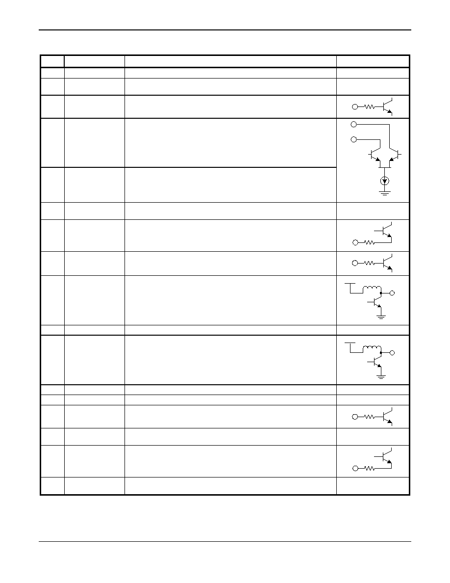
Table 1. RF25L Pin Assignments and Signal Descriptions (1 of 3)
Pin #
Name
Description
Equivalent Circuit
1 NC
No
connection
2
VCC_IF
Supply voltage for the VGA, IF mux, and bias circuitry. A bypass capacitor(s) with a short trace
is required.
3
RF_GC
The gain control pin for both RF upconverters. A DC voltage of 1.0 to 2.5 V is needed to cover
the mixer RF range.
4
VGA_OUT_P
The output pin for the 130.38 MHz VGA. This is a balanced output. It should be connected to
an external bandpass filter for noise reduction. Requires an inductor choke to VCC IF on both
differential line. Both outputs are open collectors.
5
VGA_OUT_M
Complementary output to pin 4.
≠
+
6
VCC_PCS_LAST_DRV
Supply voltage for the PCS PA driver. This pin can be used to turn the last driver amplifier on
and off for a 24 dB gain step. A bypass capacitor(s) with a short trace is required.
7
CELL_POT
This pin is connected to an external resistor. The value of the resistor sets the bias current of
the cellular driver, which affects gain and Adjacent Channel Power Rejection (ACPR). The
resistor range is from 300 to 4.0K ohms.
8
DRIVER_ON
This is the driver control signal. When the pin is low, the driver is deactivated. During
transmission the pin should be high to enable the driver. Switching this pin can be used to
provide a 33 dB step in cellular CDMA mode.
9
PCS_DRV_OUT
This is the output pin for the PCS RF signal. The pin is connected to the output of the PCS
driver amplifier. Impedance matching is required.
Vcc
10
VCC_BIAS
Supply voltage. A bypass capacitor(s) with a short trace is required.
11
CELL_DRV_OUT
This is the output pin for the cellular RF signal. The pin is connected to the output of the
cellular driver amplifier. Impedance matching is required.
Vcc
12 NC
No
connection
13 NC
No
connection
14
BAND_SELECT
This is a control signal input pin that selects between the cellular band and PCS band. When
the input is low, the cellular band is chosen. When the input is high, the PCS band is chosen.
15
VCC_CELL_DRV
Supply voltage for the of the cellular band driver. A bypass capacitor(s) with a short trace is
required.
16
PCS_POT
This pin is connected to an external resistor. The value of the resistor sets the bias current of
the PCS driver, which affects gain and ACPR. The resistor range is from 100 to 2.0K ohms.
17
VCC_PCS_MID
Supply voltage for the first amplifier in the PCS driver block. A bypass capacitor(s) with a short
trace is required.

Tx ASIC for CDMA, AMPS, and PCS Applications
RF25L
101174B
Skyworks ≠ Preliminary
5
January 14, 2002
Proprietary Information and Specifications are Subject to Change
Table 1. RF25L Pin Assignments and Signal Descriptions (2 of 3)
Pin #
Name
Description
Equivalent Circuit
18
CELL_DRV_IN
The cellular driver input. Impedance matching is required.
19
PCS_DRV_IN
The PCS driver input. Impedance matching is required.
Vcc
+
≠
20
I_DATA_P
The I/Q modulator baseband balanced input for the I channel. A typical 1.85V DC bias must be
supplied to the pin.
21
I_DATA_M
Same as pin 20, except complementary input.
≠
+
22
VCC_IQ_MOD
Supply voltage for the I/Q modulator. A bypass capacitor(s) with a short trace is required.
23
Q_DATA_P
The I/Q modulator baseband balanced input for the Q channel. A typical 1.85V DC bias must
be supplied to the pin.
24
Q_DATA_M
Same as pin 23, except complementary input.
≠
+
25 NC
No
connection
26 NC
No
connection
27 NC
No
connection
28
PCS_MIX_OUT
PCS upconverter output. This pin requires impedance matching.
Vcc
29
VCC_DIFF_DRV
Supply voltage for a differential amplifier in the upconverter block. A bypass capacitor(s) with a
short trace is required.
30
CHIP_ENABLE
This is the IQ modulator, VGA, and upconverter enable signal. When the input is low, the chip
is disabled. When the input is high, the chip is enabled.
31
CELL_MIX_OUT
Cellular upconverter output. Impedance matching required
Vcc
32
VCC_DIV
Supply voltage for the PLL divider and VCO buffer. A bypass capacitor(s) with a short trace is
required.
33 NC
No
connection
34
PLL_P
This is a balanced output for the VCO. This output goes to an external PLL that locks the VCO
frequency.
35
PLL_M
Same as pin 34, except complementary input
≠
+
Vcc
Vcc