 | –≠–ª–µ–∫—Ç—Ä–æ–Ω–Ω—ã–π –∫–æ–º–ø–æ–Ω–µ–Ω—Ç: RM009-NN | –°–∫–∞—á–∞—Ç—å:  PDF PDF  ZIP ZIP |

Data Sheet
Skyworks Solutions, Inc. Proprietary
101258B
© 1999≠2002, Skyworks Solutions, Inc., All Rights Reserved.
July 26, 2002
RM009
Power Amplifier Module for Dual-band GSM900 DCS1800
The RM009 is a dual-band Power Amplifier Module (PAM) designed in a compact
form factor for Class 4 GSM900 and Class 1 DCS1800 cellular handsets.
The module consists a GSM900 PA block and a DCS1800 PA block, matching
circuitry for 50
input and output impedances, and bias control circuitry. Two
separate Heterojunction Bipolar Transistor (HBT) PA blocks are fabricated on a
single Gallium Arsenide (GaAs) die. One PA block operates in the GSM900 band
and the other supports the DCS1800 band. The PAM is optimized for three-cell
operation with both PAs sharing common power supply pins to distribute
current. A custom CMOS integrated circuit contains a current amplifier that
minimizes the required power control current (I
APC
) to 60
µA, typical.
RF input and output ports are internally matched to 50
to reduce the number of
external components for a dual-band design. Switching circuitry receives the
band select signal on the band select pin (BS) to switch between GSM (logic 0)
and DCS (logic 1). Analog Power Control (APC) controls the output power of
each PA selected by the band select signal. The extremely low leakage current
(2
µA, typical) of the RM009 dual-band module maximizes handset standby time.
The functional block diagram shows the relationship of the dual PAs and the
CMOS device in the RM009.
Functional Block Diagram
CMOS
Bias
Controller
GSM IN
GSM OUT
DCS IN
DCS OUT
Power Control
Band Select
HBT
Match
Match
Match
Match
Distinguishing Features
∑
High efficiency
GSM 54%
DCS 45%
∑
Input/output matching
50
internal
∑
Small outline
9.1 mm x 11.6 mm
∑
Low profile
1.50 mm ±10%
∑
Low APC current
60
µA
Applications
∑
Class 4 GSM900 and Class 1
DCS1800 dual-band cellular
handsets
Electrical Specifications
RM009
Power Amplifier Module for Dual-band GSM900 DCS1800 Applications
2
Skyworks Solutions, Inc. Proprietary
101258B
July 26, 2002
Electrical Specifications
Table 1
provides the absolute maximum ratings of the RM009,
Table 2
shows the recommended
operating conditions and
Table 3
shows the electrical characteristics.
Table 1. Absolute Maximum Ratings
Parameter
Minimum
Maximum
Unit
Supply Voltage (V
CC
)
--
7
V
Storage Temperature
≠55
+125
∞C
Table 2. Recommended Operating Conditions
Parameter
Minimum
Typical
Maximum
Unit
Supply Voltage (V
CC
)
2.7
3.2
4.5
V
Temperature
≠30
--
+85
∞C
Table 3. RM009 Electrical Specifications (1 of 2)
Parameter
Symbol
Test Condition
Minimum Typical Maximum Units
GSM Mode (f = 880 MHz to 915 MHz and P
IN
= 8 dBm to 12 dBm)
Frequency Range GSM900
f
1
--
880
--
915
MHz
Input Power GSM900
P
INGSM
--
8
10
12
dBm
Leakage Current
I
LEAKAGE
V
CC
= 4.5 V
V
APC
= 0 V
V
BS
= 0 V
--
5
--
µA
Efficiency GSM900
GSM
P
INGSM
= 10 dBm
46
54
--
%
GSM 2nd and 3rd Harmonic
Distortion
H
2GSM
P
OUTGSM
= 34.5 dBm
≠39.5
≠
45
--
dBc
Output Power GSM900
P
OUTGSM
P
INGSM
= 10 dBm
34.5
35
--
dBm
P
OUTGSM
P
INGSM
= 10 dBm
V
CC
= 2.7 V
T
CASE
= ≠20 ∞C to +85 ∞C
32
--
--
dBm
Input VSWR
VSWR
(IN)
All
--
1.5:1
2:1
--
Isolation GSM900
--
P
INGSM
= 10 dBm
APC= 0.2 V
--
≠40
≠
30
dBm
Cross Isolation
--
P
OUTGSM
= 34.5 dBm
--
≠30
≠
25
dBm
Noise Floor GSM900
--
P
INGSM
= 10 dBm,
BW = 100 kHz,
fo ±20 MHz offset
--
--
≠84
dBm
Bandselect Thresholds:
GSM
DCS
V
BSLMAX
V
BSHMIN
--
2.0
--
0.5
V
V
RM009
Electrical Specifications
Power Amplifier Module for Dual-band GSM900 DCS1800 Applications
101258B
Skyworks Solutions, Inc. Proprietary
3
July 26, 2002
Full Power Control Voltage
--
P
OUTGSM
= 34.5 dBm
--
2.0
--
--
Rise Time and Fall Time
--
P
OUTGSM
= 34.5 dBm
--
1.8
--
µsec
DCS Mode (f = 1710 MHz to 1785 MHz and P
IN
= 6 dBm to 10 dBm)
Frequency Range DCS1800
f
2
--
1710
--
1785
MHz
Input Power DCS1800
P
INDCS
--
6
8
10
dBm
Control Voltage Range
V
APC
--
0.2
--
2.7
V
Control Current Into Vapc
l
APC
--
--
60
--
µA
Leakage Current
I
LEAKAGE
V
CC
= 3.2 V
V
APC
= 0 V
V
BS
= 0 V
--
5
--
µA
Efficiency DCS1800
DCS
P
INDCS
= 8 dBm
38.2
45.0
--
%
DCS 2nd and 3rd Harmonic
Distortion
H
2DCS
P
OUTDCS
= 31.5 dBm
≠40.5
≠
50
--
dBc
Output Power DCS1800
P
OUTDCS
P
INDCS
= 8 dBm
31.5
32
--
dBm
P
OUTDCS
P
INDCS
= 8 dBm
V
CC
= 2.7 V
T
CASE
= ≠20 ∞C to +85 ∞C
29.5
--
--
dBm
Input VSWR
VSWR
(IN)
All
--
1.5:1
2:1
--
Isolation DCS1800
--
P
INDCS
= 8 dBm
APC = 0.2 V
--
≠45
≠33
dBm
Stability Condition VSWR
(LOAD)
(no spurious oscillation > ≠35 dBm)
--
--
--
--
8:1
all
angles
--
Load Mismatch VSWR
(LOAD)
(no damage/degradation)
--
--
--
--
10:1
all
angles
--
Noise Floor DCS1800
--
P
INDCS
= 8 dBm
BW = 100 kHz
fo ±20 MHz offset
--
--
≠76
dBm
Full Power Control Voltage
--
P
OUTDCS
= 31.5 dBm
--
2.0
--
--
Bandselect Thresholds:
GSM
DCS
V
BSLMAX
V
BSHMIN
--
2.0
--
0.5
V
V
Rise Time and Fall Time
--
P
OUTDCS
= 31.5 dBm
--
1.8
--
µsec
NOTE(S):
T
CASE
= 25 ∞C, RL = 50
, pulsed operation with pulse width = 577 µsec and duty cycle of 1:8, V
CC
= 3.2 V,
unless specified otherwise
Table 3. RM009 Electrical Specifications (2 of 2)
Parameter
Symbol
Test Condition
Minimum Typical Maximum Units

Electrical Specifications
RM009
Power Amplifier Module for Dual-band GSM900 DCS1800 Applications
4
Skyworks Solutions, Inc. Proprietary
101258B
July 26, 2002
Figure 1. Typical RM009 Application
BS (from Baseband)
G S M I N
DCS IN
A P C f r o m P A C
10 pF
33 pF
DCS OUT
G S M O U T
2
4
1 0
1 2
1 6
1 4
VCC2
VCC1
8
6
A P C
101258_003
R M 0 0 9
CMOS
Bias
Controller
HBT
Match
Match
Match
Match
10 nF
100 pF
9
GND
10
µF
ELECTROLYTIC
Vbat
C
A
A
B
B
V
CC
Place caps at closest proximity to PA module with the capacitor ground directly connected to the PAM grounds.
Optional depending on PAC circuit.
Common connect V
bat
to all V
CC
pins.
A
B
C
C
10 pF
RM009
Package Dimensions and Pin Descriptions
Power Amplifier Module for Dual-band GSM900 DCS1800 Applications
101258B
Skyworks Solutions, Inc. Proprietary
5
July 26, 2002
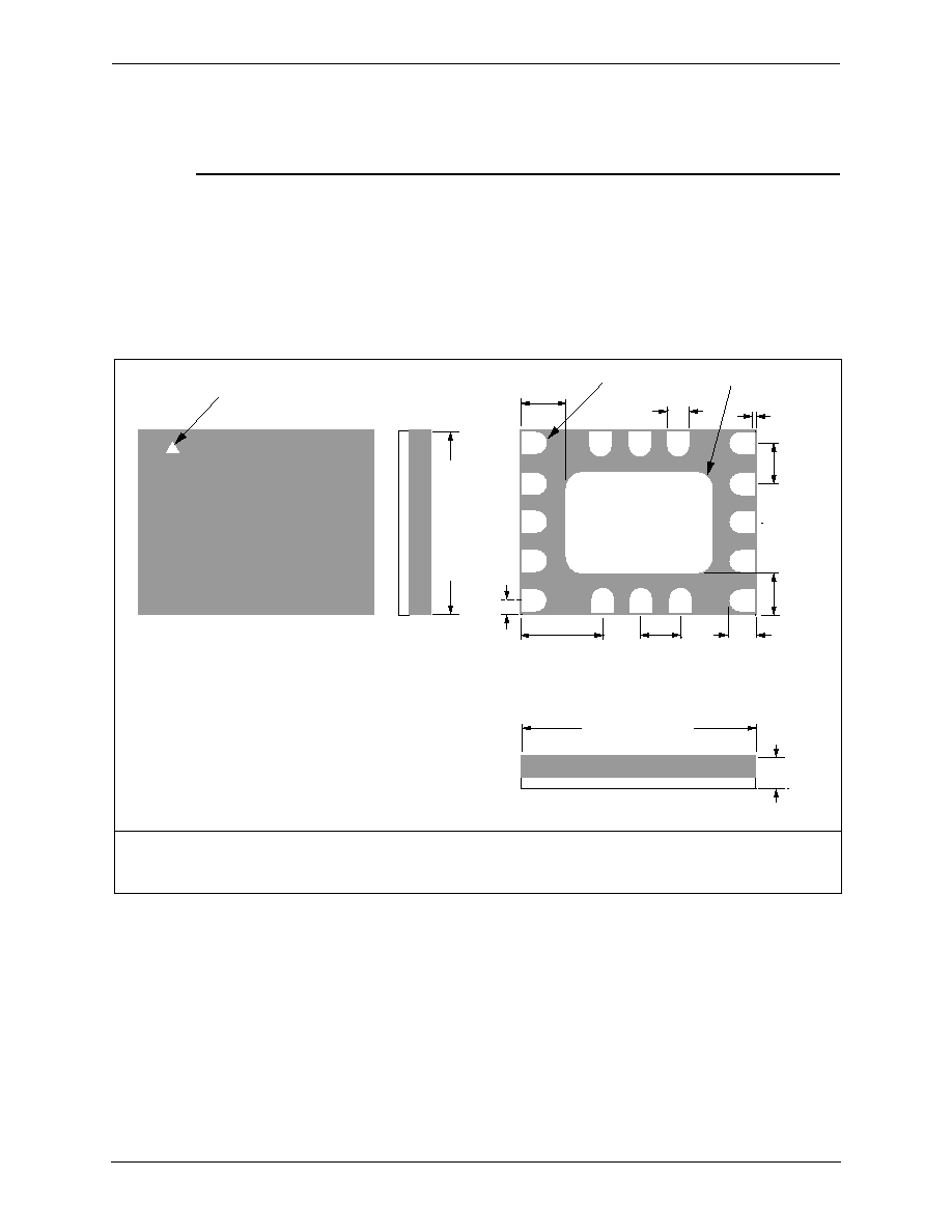
Package Dimensions and Pin Descriptions
Figure 2
is a mechanical diagram of the pad layout for the 16-pin leadless, RM009 Power
Amplifier module.
Figure 3
shows the device pin configuration and the pin numbering convention,
which starts with pin 1 in the upper left and increments counter-clockwise around the package. Pin
assignments and their functional descriptions are listed in
Table 4
.
Figure 4
shows typical case
markings.
Figure 2. RM009 PAM Package Dimensions--16-Pin Leadless Module (All Views)
SIDE VIEW
TOP VIEW
BOTTOM VIEW
FRONT VIEW
R0.381 Typ
0.762 Typ
1.02 Typ
2.286 ± 0.051
2.286 ± 0.051
PIN 1
0.127 Ref
1.905
± 0.051
3.899
± 0.051
1.55 ± 10%
R0.860 Typ
NOTE(S):
1. All contact points are gold plated, lead free-surfaces.
2. All dimensions are in millimeters.
9.10 +0.20, -0.08
11.60 +0.20/-0.08
1.905 ± 0.051
0.737 ± 0.051
101058_004