 | –≠–ª–µ–∫—Ç—Ä–æ–Ω–Ω—ã–π –∫–æ–º–ø–æ–Ω–µ–Ω—Ç: RM806-NN | –°–∫–∞—á–∞—Ç—å:  PDF PDF  ZIP ZIP |
Data Sheet
100602G
© 2001, Skyworks Solutions, Inc., All Rights Reserved.
February 7, 2002
RM806
Power Amplifier Module for TDMA AMPS (824≠849 MHz)
The dual-mode RM806 Power Amplifier (PA) is a fully matched, 6-pin, surface mount
module designed for Time Division Multiple Access (TDMA) and Advanced Mobile
Phone Service (AMPS) mobile units operating in the 824-849 MHz cellular bandwidth.
This device meets stringent IS-136 linearity requirements beyond 30 dBm output
power and can be driven to power output levels beyond 31 dBm for high efficiency FM
mode operation. A single GaAs (GaAs) Microwave Monolithic Integrated Circuit
(MMIC) contains all active circuitry in the module. The MMIC contains onboard bias
circuitry as well as input and interstage matching circuits. The output match is
realized off-chip within the module package to optimize efficiency and power
performance into a 50 ohm load. This device is manufactured using Skyworks' GaAs
Heterojunction Bipolar Transistor (HBT) process, which provides for all positive
voltage DC supply operation while maintaining high efficiency and good linearity.
Primary bias to the RM806 can be supplied directly from a three-cell nickel cadmium,
a single-cell lithium-ion battery, or any other suitable battery with output in the
3 to 4 volts range. Power down is accomplished by setting the low current reference
pin to zero volts. No external supply side switch is needed as typical "off" leakage is a
few microamperes with full primary voltage supplied from the battery.
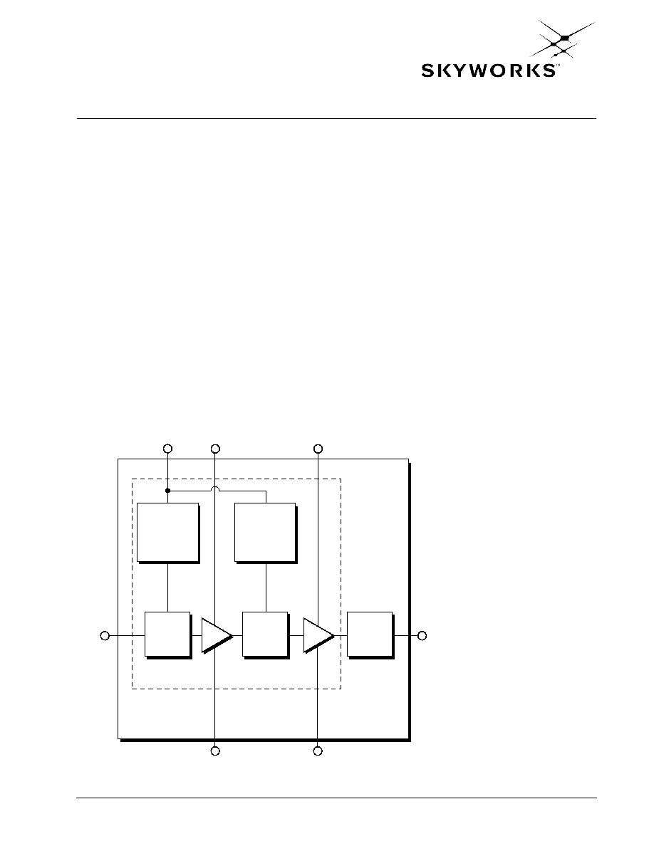
Functional Block Diagram
MMIC
MODULE
RFIN
(2)
RFOUT
(5)
VCC1
GND
GND
VCC2
VREF
Driver
Stage Bias
Power
Stage Bias
DA
Inter
Stage
Match
PA
Output
Match
(6, 7)
(3)
(1)
(4)
(6, 7)
Input
Match
Distinguishing Features
∑
Low voltage positive bias supply
∑
Good linearity
∑
High efficiency
∑
Dual mode operation
∑
Large dynamic range
∑
6-pin package
(6 mm x 6mm x 1.5 mm)
∑
Power down control
Applications
∑
Digital cellular (TDMA)
∑
Analog cellular (AMPS)
∑
Wireless local loop (WLL)
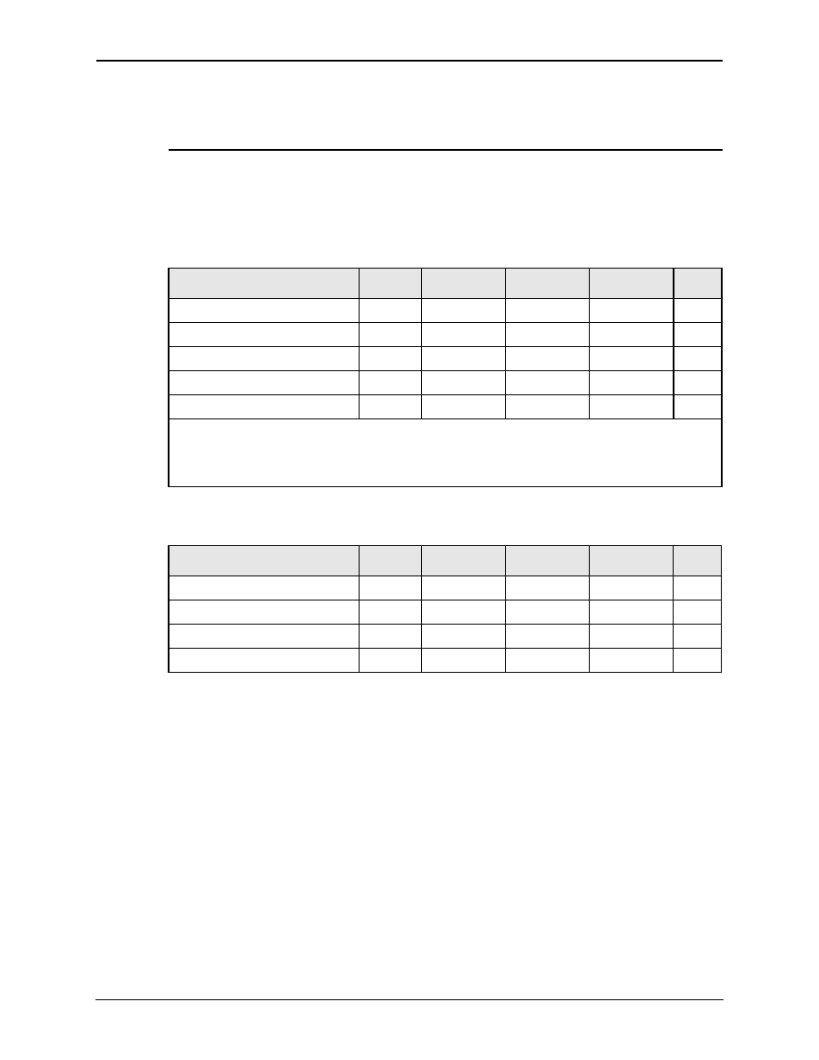
Electrical Specifications
RM806
Power Amplifier Module for TDMA AMPS (824≠849 MHz)
2
Skyworks
100602G
February 7, 2002
Electrical Specifications
The following tables list the electrical characteristics for the RM806 Power Amplifier.
Table 1
lists
the absolute maximum rating for continuous operation.
Table 2
lists the recommended operating
conditions for achieving the electrical performance listed in
Table 4
.
Table 1. Absolute Maximum Ratings
(1)
Parameter
Symbol
Minimum
Nominal
Maximum
Unit
RF Input Power
Pin
--
3.0
8.0
dBm
Supply Voltage
Vcc
--
3.4
5.0
(2)
Volts
Reference Voltage
Vref
--
3.1
3.3
Volts
Case Operating Temperature
Tc
≠30
+25
+110
∞C
Storage Temperature
Tstg
≠55
--
+125
∞C
NOTE(S):
(1)
No damage assuming only one parameter is set at limit at a time with all other parameters set at or below
nominal value.
(2)
Under pulsed TDMA modulated mode, operation at maximum supply voltage of 6.2 V up to 100 ms.
Table 2. Recommended Operating Conditions
Parameter
Symbol
Minimum
Nominal
Maximum
Unit
Supply Voltage
Vcc
3.0
3.4
4.2
Volts
Reference Voltage
Vref
3.0
3.1
3.3
Volts
Operating Frequency
Fo
824
836.5
849
MHz
Operating Temperature
To
≠30
+25
+85
∞C

RM806
Electrical Specifications
Power Amplifier Module for TDMA AMPS (824≠849 MHz)
100602G
Skyworks
3
February 7, 2002
Table 3. Electrical Specifications for TDMA / AMPS Nominal Operating Conditions
(1)
Characteristics
Condition
Symbol Minimum
(2)
Typical
Maximum
(2)
Unit
Quiescent current
--
I
q
--
150.0
165.0
mA
Reference current
Po
32 dBm
I
ref
--
6.3
7.0
mA
Leakage current
PA Off
--
--
2.0
25.0
uA
Gain≠Analog
Po = 0 dBm
Po = 31 dBm
G
G
p
29.5
28.5
30.5
30.0
32.0
31.0
dB
dB
Gain≠Digital
Po = 0 dBm
Po = 30 dBm
G
G
p
29.5
28.5
30.5
30.0
32.0
31.0
dB
dB
Power Added Efficiency
Analog Mode
Digital Mode
Po = 31 dBm
Po = 30 dBm
PAEa
PAEd
43.0
38.0
45.0
42.0
--
--
%
%
Adjacent Channel Power
(3)
30 kHz Offset
60 kHz Offset
90 kHz Offset
Po
30 dBm
Po
30 dBm
Po
30 dBm
ACP1
ACP2
ACP3
--
--
--
≠30.5
≠52.5
≠62.0
≠29.0
≠50.0
≠52.0
dBc
dBc
dBc
Harmonics
Second
Third
Po
31 dBm
Po
31 dBm
H2
H3
--
--
≠50
≠42
≠43.0
≠40.0
dBc
dBc
PA "Turn Off Time"
--
--
--
10
--
µs
PA "Turn On Time"
--
--
--
10
--
µs
Noise Power in RX Band
869-894 MHz
(4)
Po
31 dBm
Np
--
≠136.5
≠133.0
dBm/Hz
Noise Figure
--
NF
--
5.5
7.0
dB
Input VSWR
--
VSWR
--
1.5:1
1.6:1
--
Stability (Spurious output)
5:1 VSWR
All phases
S
--
--
≠60
dBc
Ruggedness--No damage
Po
31 dBm
Ru
--
--
8:1
VSWR
NOTE(S):
(1)
Vcc = +3.4 V, Vref = +3.1 V, Freq = 836.5 MHz, Tc = 25 ∞C.
(2)
Min/Max values indicate performance over process corners and conditions specified in note 1 above unless
otherwise detailed.
(3)
Also meets same linearity for Po
28.5 dBm @ Vcc = +3.0 V.
(4)
With NADC modulation applied.

Electrical Specifications
RM806
Power Amplifier Module for TDMA AMPS (824≠849 MHz)
4
Skyworks
100602G
February 7, 2002
Table 4. Electrical Specifications for TDMA / AMPS Nominal Operating Conditions
(1)
Characteristics
Condition
Symbol Minimum
(2)
Typical
Maximum
(2)
Unit
Quiescent current
--
I
q
--
150.0
185.0
mA
Reference current
Po
32 dBm
I
ref
--
6.3
7.6
mA
Leakage current
(4)
PA Off
--
--
2.0
25.0
uA
Gain≠Analog
Po = 0 dBm
Po = 31 dBm
G
G
p
27.5
26.0
30.5
30.0
33.0
33.0
dB
dB
Gain≠Digital
Po = 0 dBm
Po = 30 dBm
G
G
p
27.5
26.0
30.5
30.0
32.5
32.5
dB
dB
Power Added Efficiency
Analog Mode
Digital Mode
Po = 31 dBm
Po = 30 dBm
PAEa
PAEd
41.0
37.0
45.0
42.0
--
--
%
%
Adjacent Channel Power
(2)
30 kHz Offset
60 kHz Offset
90 kHz Offset
Po
30 dBm
Po
30 dBm
Po
30 dBm
ACP1
ACP2
ACP3
--
--
--
≠30.5
≠52.5
≠62.0
≠27.0
≠46.0
≠50.0
dBc
dBc
dBc
Harmonics
Second
Third
Po
31 dBm
Po
31 dBm
H2
H3
--
--
≠50
≠42
≠35.0
≠35.0
dBc
dBc
PA "Turn Off Time"
--
--
--
10.0
30.0
µs
PA "Turn On Time"
--
--
--
10.0
30.0
µs
Noise Power in RX Band
869-894 MHz
(3)
Po
31 dBm
Np
--
≠136.5
≠132.0
dBm/Hz
Noise Figure
--
NF
--
5.5
8.0
dB
Input VSWR
--
VSWR
--
1.5:1
2.0:1
--
Stability (Spurious output)
(4)
5:1 VSWR
All phases
S
--
--
≠60
dBc
Ruggedness--No damage
(4)
Po
31 dBm
Ru
--
--
8:1
VSWR
NOTE(S):
1. Min/Max values indicate performance over process corners and conditions specified in note
(1)
below unless
otherwise detailed.
(1)
Per Table 3 with Vcc = +3.4 V.
(2)
Also meets same linearity for Po
28.5 dBm @ Vcc = +3.0 V and as further specified in note
(1)
above.
(3)
With NADC modulation applied. Tc = 25 ∞C
(4)
Tc = 25 ∞C
RM806
Characterization Data
Power Amplifier Module for TDMA AMPS (824≠849 MHz)
100602G
Skyworks
5
February 7, 2002
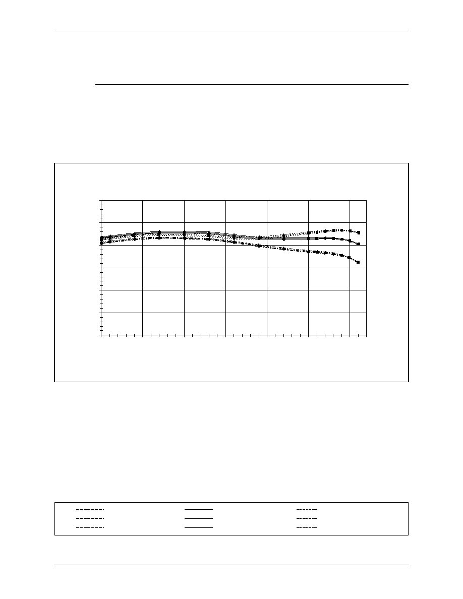
Characterization Data
The following graphs illustrate characteristics for a typical RM806 Power Amplifier. The amplifier
was selected by characterizing a group of devices and selecting a part having average electrical
performance both at nominal and worst case.
Figures 1
through
5
illustrate the digital signal
characteristics and
Figures 6
through
9
illustrate the analog characteristics for the RM806.
Legend
Figure 1. Digital Gain vs. Output Power
20.0
22.5
25.0
27.5
30.0
32.5
35.0
0
5
10
15
20
25
30
Output Power (dBm)
Ga
in
(dB
)
Vref = 3.1 V, Vcc = 3.4 V
824 MHz @ ≠30
∞C
824 MHz @ +25
∞C
824 MHz @ +85
∞C
837 MHz @ ≠30
∞C
837 MHz @ +25
∞C
837 MHz @ +85
∞C
849 MHz @ ≠30
∞C
849 MHz @ +25
∞C
849 MHz @ +85
∞C
824 MHz @ ≠30
∞C
824 MHz @ +25
∞C
824 MHz @ +85
∞C
837 MHz @ ≠30
∞C
837 MHz @ +25
∞C
837 MHz @ +85
∞C
849 MHz @ ≠30
∞C
849 MHz @ +25
∞C
849 MHz @ +85
∞C