 | –≠–ª–µ–∫—Ç—Ä–æ–Ω–Ω—ã–π –∫–æ–º–ø–æ–Ω–µ–Ω—Ç: SMP1321 | –°–∫–∞—á–∞—Ç—å:  PDF PDF  ZIP ZIP |
Skyworks Solutions, Inc. ∑ Phone [781] 376-3000 ∑ Fax [781] 376-3100 ∑ sales@skyworksinc.com ∑ www.skyworksinc.com
200048 Rev. B ∑ Skyworks Proprietary Information ∑ Products and Product Information are Subject to Change Without Notice. ∑ October 25, 2004
1
SMP1321 Series: Low Capacitance
Plastic Packaged PIN Diodes
DATA SHEET
Features
Designed for high performance wireless switch applications
0.25 pF capacitance specified
Available lead (Pb)-free MSL-1 @ 250 ∞C per JEDEC J-STD-020
Available in tape and reel packaging
Description
The SMP1321 series of plastic packaged, surface mountable PIN
diodes are designed for high volume switch applications from
10 MHz to beyond 2 GHz. The low capacitance of these diodes
(0.25 pF) combined with its low resistance (2.0
maximum at
10 mA) make the SMP1321 series particularly suited to high
isolation series connected PIN diode switches in battery operated
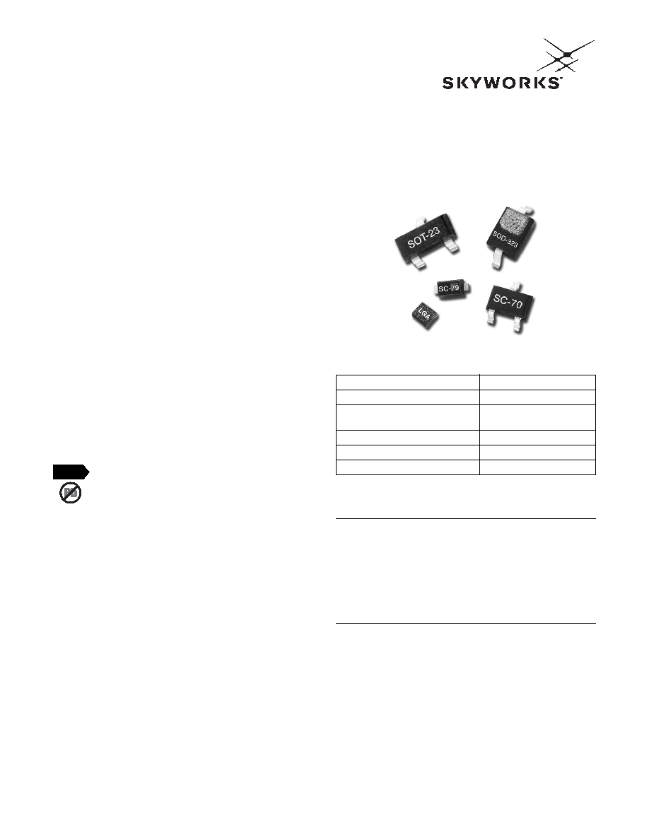
circuits. Available in a selection of plastic packages and in a
variety of configurations including a low inductance (0.4 nH)
SOT-23 (SMP1321-007), the small footprint SC-79 and the minia-
ture SC-70. The SMP1321-508 has been specifically designed for
WLAN 802.11 a, b, and g applications.
Characteristic
Value
Reverse voltage (V
R
)
100 V
Power dissipation @ 25 ∞C lead
250 mW
temperature (P
D
)
Storage temperature (T
ST
)
-65 ∞C to +150 ∞C
Operating temperature (T
OP
)
-65 ∞C to +150 ∞C
ESD human body model
Class 1B
Absolute Maximum Ratings
Skyworks offers lead (Pb)-free "environmentally
friendly" packaging that is RoHS compliant
(European Parliament for the Restriction of
Hazardous Substances).
NEW
Performance is guaranteed only under the conditions listed in the specifications table and is
not guaranteed under the full range(s) described by the Absolute Maximum specifications.
Exceeding any of the absolute maximum/minimum specifications may result in permanent
damage to the device and will void the warranty.
CAUTION: Although this device is designed to be as robust as
possible, Electrostatic Discharge (ESD) can damage
this device. This device must be protected at all times
from ESD. Static charges may easily produce poten-
tials of several kilovolts on the human body or
equipment, which can discharge without detection.
Industry-standard ESD precautions must be employed
at all times.

Skyworks Solutions, Inc. ∑ Phone [781] 376-3000 ∑ Fax [781] 376-3100 ∑ sales@skyworksinc.com ∑ www.skyworksinc.com
October 25, 2004 ∑ Skyworks Proprietary Information ∑ Products and Product Information are Subject to Change Without Notice. ∑ 200048 Rev. B
DATA SHEET ∑ SMP1321 SERIES
2
Common Common
Low
Single
Anode
Cathode
Series Pair
Inductance
Single
Single
Anti-Parallel
SOT-23
SOT-23
SOT-23
SOT-23
SOT-23
SOD-323
SC-79
LGA
SMP1321-001
SMP1321-003
SMP1321-004
SMP1321-005
SMP1321-007
SMP1321-011
SMP1321-079
SMP1321-508
Lead (Pb)-Free
Marking: PM1
Marking: PM9
Marking: PM3
Marking: PM2
Marking: PMB
Marking: PM
Marking: H
SMP1321-003LF
SMP1321-004LF
SMP1321-005LF
SMP1321-011LF
SMP1321-079LF
Marking: RM9
Marking: RM3
Marking: RM2
Marking: RM
L
S
= 1.5 nH
L
S
= 1.5 nH
L
S
= 1.5 nH
L
S
= 1.5 nH
L
S
= 0.4 nH
L
S
= 1.5 nH
L
S
= 0.7 nH
L
S
= 0.6 nH
SC-70
SC-70
SC-70
SMP1321-073
SMP1321-074
SMP1321-075
Marking: PM9
Marking: PM2
Marking: PMB
L
S
= 1.4 nH
L
S
= 1.4 nH
L
S
= 1.4 nH
LF denotes lead (Pb)-free packaging option as an alternative to our standard
tin/lead (Sn/Pb) packaging.
Parameter
Condition
Typ.
Max.
Unit
Reverse current (I
R
)
V
R
= 100 V
10
µA
Capacitance (C
T
)
(1)
F = 1 MHz, V = 30 V
0.25
pF
Resistance (R
S
)
F = 100 MHz, I = 1 mA
3.00
Resistance (R
S
)
F = 100 MHz, I = 10 mA
2.00
Forward voltage (V
F
)
I
F
= 10 mA
0.85
V
Carrier lifetime (TI)
I
F
= 10 mA
0.40
µs
I region width
15
µm
Electrical Specifications at 25 ∞C
1. The SMP1321-007 maximum capacitance is 0.40 pF.

DATA SHEET ∑ SMP1321 SERIES
Skyworks Solutions, Inc. ∑ Phone [781] 376-3000 ∑ Fax [781] 376-3100 ∑ sales@skyworksinc.com ∑ www.skyworksinc.com
200048 Rev. B ∑ Skyworks Proprietary Information ∑ Products and Product Information are Subject to Change Without Notice. ∑ October 25, 2004
3
Series Resistance vs. Current @ 100 MHz
0.01
0.1
1
10
100
Forward Current (mA)
Series Resistance (
)
0.1
1
10
100
0
1
2
5
10
20
50
Capacitance vs. Reverse Voltage
0
0.2
0.1
0.4
0.6
0.5
0.3
0.8
0.7
Reverse Voltage (V)
Capacitance (pF)
1 MHz≠1 GHz
400
500
600
700
800
900
1000
DC Characteristic
0.01
0.1
1
10
100
Forward Voltage (mV)
Forward Current (mA)
0
500
1000
1500
2000
Conductance vs. Frequency and Reverse Voltage
Frequency (MHz)
Conductance (
µ
S)
0 V
10 V
40 V
0
100
200
300
400
500
600
700
800
Typical Performance Data
R
R
R
R
R
I
F
-55 ∞C
-15 ∞C
+25 ∞C
+65 ∞C
+100 ∞C
(mA)
(
)
(
)
(
)
(
)
(
)
0.02
47.400
50.000
56.300
61.500
65.100
0.10
12.000
12.600
13.900
15.400
16.400
0.30
5.200
5.400
5.800
6.400
6.900
0.50
3.600
3.800
4.100
4.500
4.800
1.00
2.400
2.500
2.600
2.800
3.100
10.00
1.030
1.040
1.040
1.070
1.150
20.00
0.871
0.888
0.873
0.889
0.956
100.00
0.669
0.659
0.642
0.645
0.695
Resistance vs. Temperature @ 500 MHz
SMP1321-007
In the -007 configuration of the SOT-23 package, the package
inductance is effectively reduced to 0.4 nH, in comparison to the
1.5 nH value of the standard configuration. This lower inductance
will be particularly beneficial when the diodes are used as shunt
connected switches at frequencies higher than 500 MHz, where
inductance is the primary limitation on maximum switch isolation.
To achieve the effective 0.4 nH, the SOT-23 package must
be inserted in the microstrip circuit board with a gap in the
trace, as shown in the figure. Because of the polarity of the
diode junction, this low
inductance feature is only
realizable with the cathode
connected to ground.
Ground
Gap

Skyworks Solutions, Inc. ∑ Phone [781] 376-3000 ∑ Fax [781] 376-3100 ∑ sales@skyworksinc.com ∑ www.skyworksinc.com
October 25, 2004 ∑ Skyworks Proprietary Information ∑ Products and Product Information are Subject to Change Without Notice. ∑ 200048 Rev. B
DATA SHEET ∑ SMP1321 SERIES
4
SOT-23
3
2
1
0.035 (0.89 mm) Min.
0.044 (1.12 mm) Max.
0.0005 (0.01 mm) Min.
0.004 (0.10 mm) Max.
0.012 (0.30 mm) Min.
0.020 (0.50 mm) Max.
0.003 (0.080 mm) Min.
0.008 (0.20 mm) Max.
8∞ Max.
0.022 (0.55 mm) Ref.
0.110 (2.80 mm) Min.
0.120 (3.04 mm) Max.
0.083 (2.10 mm) Min.
0.104 (2.64 mm) Max.
0.037 (0.95 mm) Ref.
0.047 (1.20 mm) Min.
0.055 (1.40 mm) Max.
0.076 (1.92 mm) Ref.
0.020 (0.51 mm) Ref.
SOD-323
0.090 (2.30 mm) Min.
0.108 (2.74 mm) Max.
0.045 (1.15 mm) Min.
0.053 (1.35 mm) Max.
0.050
(1.25 mm) Max.
0.006
(0.15 mm) Typ.
0.008 (0.20 mm) Nom.
0.004 (0.10 mm) Max.
0.010 (0.25 mm) Min.
0.010
(0.25 mm) Min.
0.016
(0.40 mm) Max.
0.063 (1.60 mm) Min.
0.071 (1.80 mm) Max.
Cathode
Indicator
2
1
LGA
Pin 2
Pin 1
Pin 3
Pin 1
Pin 3
Pin 4
Pin 4
(1.03)
(0.73)
(0.30)
(0.00)
Pin 2
0.058 (1.47 mm)
0.054 (1.39 mm)
0.028 (0.70 mm)
0.023 (0.58 mm)
Side View
Top View
0.048 (1.23 mm)
0.044 (1.13 mm)
(0.138 x 45)
(1.27)
(0.87)
(0.40)
(0.00)
Bottom View
(0.076) All Around
SC-79
0.060 (1.50 mm) Min.
0.067 (1.70 mm) Max.
0.010
(0.25 mm) Min.
0.014
(0.35 mm) Max.
0.043 (1.10 mm) Min.
0.051 (1.30 mm) Max.
0.020
(0.50 mm) Min.
0.028
(0.70 mm) Max.
0.003
(0.07 mm) Min.
0.008
(0.20 mm) Max.
10∞ Max.
10∞ Max.
0.028
(0.70 mm) Min.
0.035
(0.90 mm) Max.
0.006 (0.15 mm) Min.
Cathode
Indicator
1
2
SC-70
3
2
1
0.031 (0.80 mm) Min.
0.039 (1.00 mm) Max.
0.000 (0.00 mm) Min.
0.004 (0.10 mm) Max.
0.010 (0.25 mm) Min.
0.016 (0.40 mm) Max.
0.071 (1.80 mm) Min.
0.087 (2.20 mm) Max.
0.071 (1.80 mm) Min.
0.094 (2.40 mm) Max.
0.045 (1.15 mm) Min.
0.053 (1.35 mm) Max.
0.026 (0.65 mm) Ref.
0.051 (1.30 mm) Ref.
0.004 (0.10 mm) Min.
0.007 (0.18 mm) Max.
0.004 (0.10 mm) Min.
0.012 (0.30 mm) Max.
0.014 (0.35 mm) Ref.

DATA SHEET ∑ SMP1321 SERIES
Skyworks Solutions, Inc. ∑ Phone [781] 376-3000 ∑ Fax [781] 376-3100 ∑ sales@skyworksinc.com ∑ www.skyworksinc.com
200048 Rev. B ∑ Skyworks Proprietary Information ∑ Products and Product Information are Subject to Change Without Notice. ∑ October 25, 2004
5
Profile Feature
SnPb Eutectic Assembly
Lead (Pb)-Free Assembly 100% Sn
Average ramp-up rate (T
L
to T
P
)
3 ∞C/second max.
3 ∞C/second max.
Preheat
Temperature min. (T
SMIN
)
100 ∞C
150 ∞C
Temperature max. (T
SMAX
)
150 ∞C
200 ∞C
Time (min. to max.) (ts)
60≠120 seconds
60≠80 seconds
T
SMAX
to T
L
Ramp-up rate
--
3 ∞C/second max.
Time maintained above:
Temperature (T
L
)
183 ∞C
217 ∞C
Time (t
L
)
60≠150 seconds
60≠150 seconds
Peak temperature (T
P
)
240 +0/-5 ∞C
250 +0/-5 ∞C
Time within 5 ∞C of actual peak temperature (tp)
10≠30 seconds
20≠40 seconds
Ramp-down rate
6 ∞C/second max.
6 ∞C/second max.
Time 25 ∞C to peak temperature
6 minutes max.
8 minutes max.
Recommended Solder Reflow Profiles
T
P
T
SMAX
T
SMIN
t
s
Preheat
t
p
Critical Zone
T
L
to T
L
t 25 ∞C to Peak
Time
T
empera
ture
T
L
25 ∞C
Reference JEDEC J-STD-020
I
L
All temperatures refer to the topside of the package, measured on the package body surface.
Reference JEDEC J-STD-020B.