Skyworks Solutions, Inc. [781] 376-3000
∑ Fax [781] 376-3100 ∑ Email sales@skyworksinc.com ∑ www.skyworksinc.com
1
Specifications subject to change without notice. 4/03A
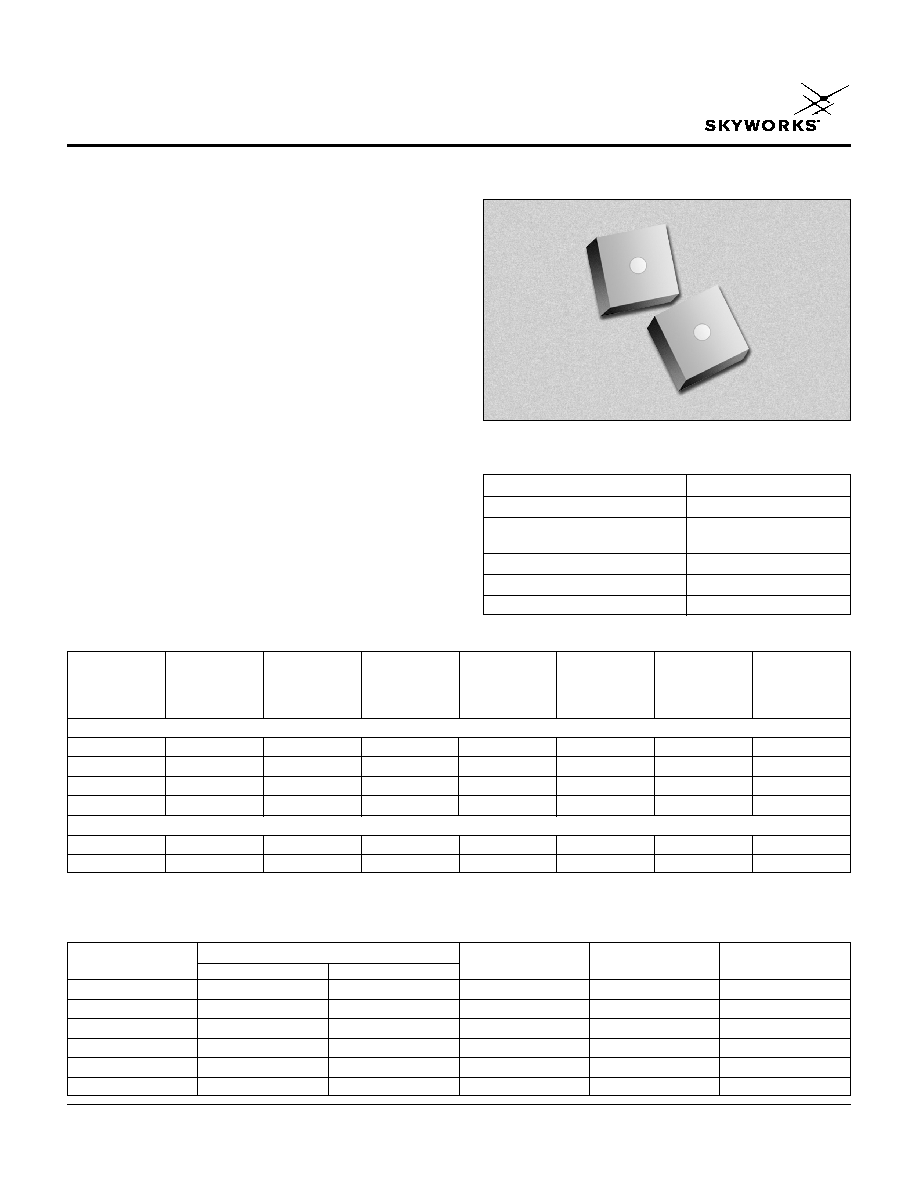
PIN Diode Chips Supplied on Film Frame
Features
Designed for High Performance Switch and
Attenuator Applications
Preferred Device for Module Applications
PIN Diodes Supplied 100% Tested, Sawn,
Mounted on Film Frame
Low Cost
Description
The SMP series of PIN diodes are designed for high
volume switch applications from 10 MHz to beyond 2 GHz.
The low current, low capacitance performance of these
diodes makes the SMP series particularly suited for
battery-operated circuits, power amplifier modules, VCO,
T/R switches and other applications. The SMP1302-099
and SMP1304-099 parts are designed as a low distortion
attenuator used in TV distribution and cellular base station
applications.
Electrical Specifications at 25∞C
Chip Dimensions
Typ. C
J
Max. C
J
Max. R
S
Max. R
S
Typical Carrier
Part
Min. V
B
V
R
= 0 V
V
R
= 10 V
Typ. V
F
I
F
= 1 mA
I
F
= 10 mA
Lifetime
Number
I
R
= 10
µ
µA
F = 1 MHz
F = 1 MHz
@ I
F
= 10 mA
F = 100 MHz
F = 100 MHz
I
F
= 10 mA
(V)
(pF)
(pF)
(mV)
(
)
(
)
(nsec)
Switching Applications
SMP1320-099
50
0.23
0.175
850
2.0 Typ.
0.9
400
SMP1322-099
50
1.10
0.850
825
1.5
0.45 Typ.
400
SMP1340-099
50
0.20
0.150
880
1.7 Typ.
1.2
100
SMP1353-099
100
0.35
0.150
825
15
2.8
1000
Attenuator Applications
SMP1302-099
200
0.27
0.15 @ 30 V
800
20
3.0
700
SMP1304-099
200
0.18
0.15 @ 30 V
800
50
7.0
1000
The above PIN diode chips are processed on 100 mm silicon wafers, 100% DC tested, sawn and shipped on 6" film frame hoops.
Electrical rejects are identified with black ink.
Quantity of Good Diodes Per Wafer
Bonding Pad
Chip Size
Chip Height
Part Number
Min.
Nom.
Nominal (In.)
Nominal (In.)
Nominal (In.)
SMP1320-099
40,000
46,000
0.003 ± 0.0003
0.0135 ± 0.001
0.0055 ± 0.0005
SMP1322-099
40,000
46,000
0.0075 ± 0.0003
0.0135 ± 0.001
0.0055 ± 0.0005
SMP1340-099
65,000
72,000
0.003 ± 0.0003
0.0110 ± 0.001
0.0055 ± 0.0005
SMP1353-099
65,000
72,000
0.008 ± 0.0005
0.0110 ± 0.001
0.0055 ± 0.0005
SMP1302-099
40,000
46,000
0.0085 ± 0.0005
0.0135 ± 0.001
0.0055 ± 0.0005
SMP1304-099
40,000
46,000
0.0085 ± 0.0005
0.0135 ± 0.001
0.0100 ± 0.0010
Characteristic
Value
Reverse Voltage (V
R
)
50 V
Power Dissipation @ 25∞C
250 mW
at the Base of the Chip
Storage Temperature
-65∞C to +150∞C
Operating Temperature
-65∞C to +150∞C
ESD Human Body Model
Class 1 B
Absolute Maximum Ratings

PIN Diode Chips Supplied on Film Frame
2
Skyworks Solutions, Inc. [781] 376-3000
∑ Fax [781] 376-3100 ∑ Email sales@skyworksinc.com ∑ www.skyworksinc.com
Specifications subject to change without notice. 4/03A
Series Resistance (
)
Forward Current (mA)
Series Resistance vs.
Forward Current @ 100 MHz
0.1
1
10
100
0.01
0.1
1
10
100
Series Resistance (
)
Forward Current (mA)
Series Resistance vs.
Forward Current @ 100 MHz
0.1
1
10
100
0.01
0.1
1
10
100
Forward Current (mA)
Forward Voltage (mV)
DC Characteristic
0.01
0.1
1
10
100
400
500
600
700
800
900
1000
Forward Current (mA)
Forward Voltage (mV)
DC Characteristic
0.01
0.1
1
10
100
0
200
400
600
800
1000
Capacitance (pF)
Reverse Voltage (V)
Capacitance vs. Reverse Voltage
0
0.05
0.10
0.15
0.20
0.25
0
5
10
15
20
25
30
Capacitance (pF)
Reverse Voltage (V)
Capacitance vs. Reverse Voltage
0
0.5
1.0
1.5
0
5
10
15
20
25
30
35
Typical Performance Data at 25∞C
SMP1320
SMP1322

PIN Diode Chips Supplied on Film Frame
Skyworks Solutions, Inc. [781] 376-3000
∑ Fax [781] 376-3100 ∑ Email sales@skyworksinc.com ∑ www.skyworksinc.com
3
Specifications subject to change without notice. 4/03A
Series Resistance (
)
Forward Current (mA)
Series Resistance vs.
Forward Current @ 100 MHz
0.1
1
10
100
0.01
0.1
1
10
100
Series Resistance (
)
Forward Current (mA)
Series Resistance vs.
Forward Current @ 100 MHz
0.1
1
10
100
1000
0.01
0.1
1
10
100
Forward Current (mA)
Forward Voltage (mV)
DC Characteristic
0.01
0.1
1
10
100
400
500
600
700
800
900
1000
Forward Current (mA)
Forward Voltage (mV)
DC Characteristic
0.01
0.1
1
10
100
400
500
600
700
800
900
1000
Capacitance (pF)
Reverse Voltage (V)
Capacitance vs. Reverse Voltage
0
5
10
15
20
25
30
0
0.05
0.10
0.15
0.20
Capacitance (pF)
Reverse Voltage (V)
Capacitance vs. Reverse Voltage
0
0.05
0.10
0.15
0.20
0.25
0.30
0
5
10
15
20
25
30
35
Typical Performance Data at 25∞C
SMP1340
SMP1353

PIN Diode Chips Supplied on Film Frame
4
Skyworks Solutions, Inc. [781] 376-3000
∑ Fax [781] 376-3100 ∑ Email sales@skyworksinc.com ∑ www.skyworksinc.com
Specifications subject to change without notice. 4/03A
Series Resistance vs. Current @ 100 MHz
0.01
0.1
1
10
100
Forward Current (mA)
Series Resistance (
)
0.1
1
10
100
1000
400
500
600
700
800
900
1000
DC Characteristic
0.01
0.1
1
10
100
Forward Voltage (mV)
Forward Current (mA)
Capacitance vs. Reverse Voltage
Reverse Voltage (V)
Capacitance (pF)
0
0.05
0.10
0.15
0.20
0.25
0
5
10
15
20
25
30
Typical Performance Data at 25∞C
SMP1302
Series Resistance vs. Current @ 100 MHz
0.01
0.1
1
10
100
Forward Current (mA)
Series Resistance (
)
0.1
1
10
100
1000
10000
400
500
600
700
800
900
1000
DC Characteristic
0.01
0.1
1
10
100
Forward Voltage (mV)
Forward Current (mA)
.
Capacitance (pF)
Reverse Voltage (V)
Capacitance vs. Reverse Voltage
0
0.05
0.10
0.15
0.20
0
5
10
15
20
25
30
SMP1304

PIN Diode Chips Supplied on Film Frame
Skyworks Solutions, Inc. [781] 376-3000
∑ Fax [781] 376-3100 ∑ Email sales@skyworksinc.com ∑ www.skyworksinc.com
5
Specifications subject to change without notice. 4/03A
Wafer On Film
GRIP RING
0.003 (0.076 mm)
SEPARATION
BETWEEN DIE
3.940 (100.0 mm)
WAFER DIA.
5.520 (140.20 mm)
INNER RING I.D.
5.981 (151.92 mm)
OUTER RING O.D.
0.236 (5.99 mm)
RING THICKNESS
0.003 (0.076 mm) NOM.
SEPARATION
BETWEEN DIE
Wafer Film Frame Description
Wafer on Nitto Tape
Color: Light Blue
Thickness: 2.2≠3.0 mils
Tensile Strength: 6.6 (lbs. in width)
Ring Material: Plastic