smp1340series.qxd
Skyworks Solutions, Inc. [781] 376-3000
· Fax [781] 376-3100 · Email sales@skyworksinc.com · www.skyworksinc.com
1
Specifications subject to change without notice. 4/03A
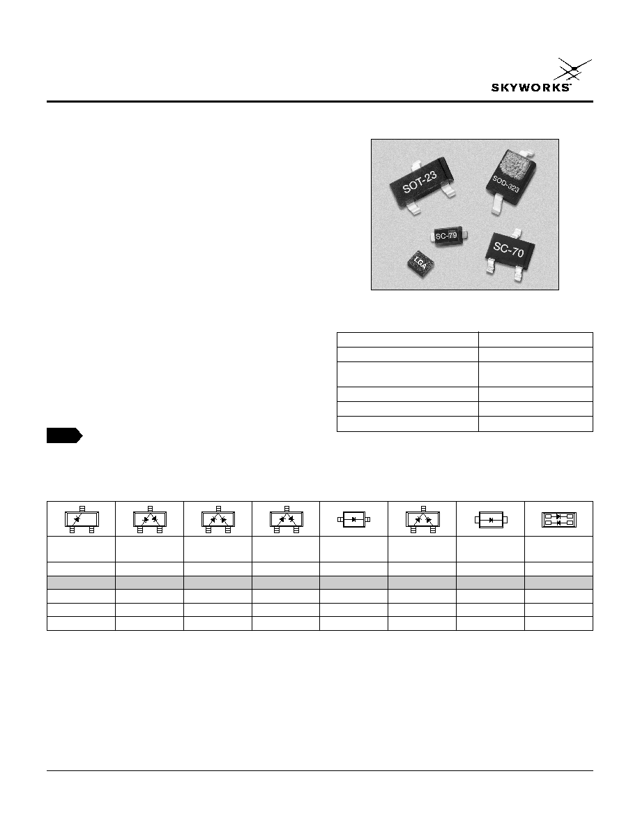
Fast Switching Speed, Low Capacitance
Plastic Packaged PIN Diodes
Features
Designed for Fast Speed Wireless Switch
Applications
1.0 Resistance, 0.3 pF Capacitance
Available Lead (Pb)-Free MSL-1 @ 250°C
per JEDEC J-STD-020
Available in Tape and Reel Packaging
Description
The SMP1340 series of plastic packaged, surface
mountable PIN diodes are designed for high volume switch
applications from 10 MHz to beyond 2 GHz. The short
carrier lifetime of typically 100 nS, combined with its thin
I region width of nominally 7
µm, results in a fast speed
RF switching PIN diode. The RF performance of the
SMP1340 series is assured by virtue of its low
capacitance (0.3 pF) and low resistance (1.0
at 10 mA).
The SMP1340-508 has been specifically designed for
WLAN 802.11 a, b, and g applications.
SMP1340 Series
Characteristic
Value
Reverse Voltage (V
R
)
50 V
Power Dissipation @ 25°C Lead
250 mW
Temperature (P
D
)
Storage Temperature (T
ST
)
-65°C to +150°C
Operating Temperature (T
OP
)
-65°C to +150°C
ESD Human Body Model
Class 1B
Absolute Maximum Ratings
LF denotes Lead (Pb)-Free packaging.
Common Common
Series
Common
Single
Anode
Cathode
Pair
Single
Cathode
Single
Anti-Parallel
Marking: PS1
Marking: PS9
Marking: PS3
Marking: PS2
Marking: PS3
Marking: X
SOT-23
SOT-23
SOT-23
SOT-23
SOD-323
SC-70
SC-79
LGA
SMP1340-001
SMP1340-003
SMP1340-004
SMP1340-005
SMP1340-011
SMP1340-074
SMP1340-079
SMP1340-508
SMP1340-079LF
L
S
= 1.5 nH
L
S
= 1.5 nH
L
S
= 1.5 nH
L
S
= 1.5 nH
L
S
= 1.5 nH
L
S
= 1.4 nH
L
S
= 0.7 nH
L
S
= 0.6 nH
Lead (Pb)-Free "environmentally friendly"
packaging available: Skyworks offers the
SMP1340-079LF and SMP1340-508 Lead
(Pb)-Free package as a green alternative.
NEW
2
Skyworks Solutions, Inc. [781] 376-3000
· Fax [781] 376-3100 · Email sales@skyworksinc.com · www.skyworksinc.com
Specifications subject to change without notice. 4/03A
Fast Switching Speed, Low Capacitance Plastic Packaged PIN Diodes
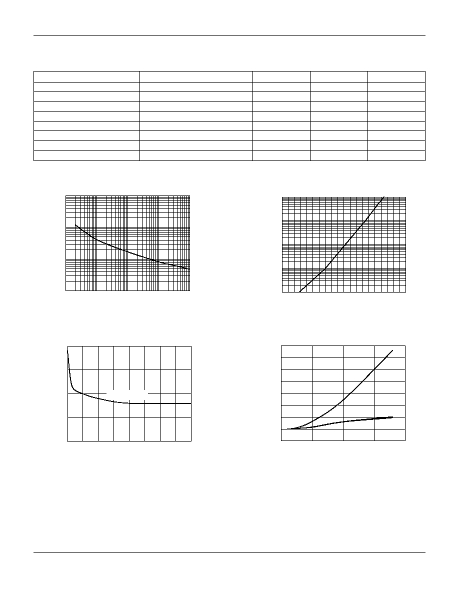
SMP1340 Series
Series Resistance vs. Current @ 100 MHz
0.01
0.1
1
10
100
Forward Current (mA)
Series Resistance (
)
0.1
1
10
100
Capacitance vs. Reverse Voltage
0.10
0.20
0.15
0.25
0.30
Reverse Voltage (V)
Capacitance (pF)
0
5
10
15
25
35
20
30
40
1 MHz1 GHz
0.6
0.7
0.8
0.9
1.0
DC Characteristic
0.01
0.1
1
10
100
Forward Voltage (mV)
Forward Current (mA)
0
500
1000
1500
2000
Conductance vs. Frequency
and Reverse Voltage
Frequency (MHz)
Conductance (
µ
S)
0 V
40 V
10 V
-50
50
0
100
150
200
250
350
300
Typical Performance Data
Parameter
Condition
Typ.
Max.
Unit
Reverse Current (I
R
)
V
R
= 50 V
10
µA
Capacitance (C
T
)
F = 1 MHz, V = 5 V
0.21
0.30
pF
Resistance (R
S
)
F = 100 MHz, I = 1 mA
1.7
Resistance (R
S
)
F = 100 MHz, I = 5 mA
1.0
2.0
Resistance (R
S
)
F = 100 MHz, I = 10 mA
0.85
1.2
Forward Voltage (V
F
)
IF = 10 mA
0.85
V
Carrier Lifetime (TI)
IF = 10 mA
100
nS
I Region Width
7
µm
Electrical Specifications at 25°C
Fast Switching Speed, Low Capacitance Plastic Packaged PIN Diodes
SMP1340 Series
Skyworks Solutions, Inc. [781] 376-3000
· Fax [781] 376-3100 · Email sales@skyworksinc.com · www.skyworksinc.com
3
Specifications subject to change without notice. 4/03A
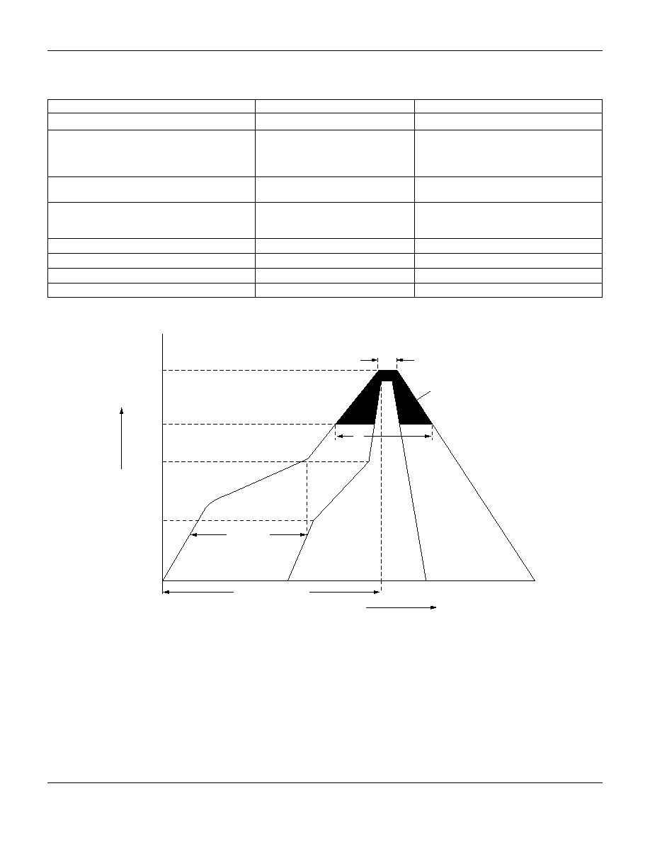
Profile Feature
SnPb Eutectic Assembly
Lead (Pb)-Free Assembly 100% Sn
Average Ramp-Up Rate (T
L
to T
P
)
3°C/Second Max.
3°C/Second Max.
Preheat
Temperature Min. (T
Smin
)
100°C
150°C
Temperature Max. (T
Smax
)
150°C 200°C
Time (Min. to Max.) (ts)
60120 Seconds
6080 Seconds
T
Smax
to T
L
Ramp-up Rate
--
3°C/Second Max.
Time Maintained Above:
Temperature (T
L
) 183°C
217°C
Time (t
L
)
60150 Seconds
60150 Seconds
Peak Temperature (T
P
)
240 +0/-5°C
250 +0/-5°C
Time Within 5°C of Actual Peak Temperature (tp)
1030 Seconds
2040 Seconds
Ramp-Down Rate
6°C/Second Max.
6°C/Second Max.
Time 25°C to Peak Temperature
6 Minutes Max.
8 Minutes Max.
Recommended Solder Reflow Profiles
T
P
T
Smax
T
Smin
t
s
Preheat
t
p
Critical Zone
T
L
to T
L
t 25°C to Peak
Time
T
emper
ature
T
L
25°C
Reference JEDEC J-STD-020
I
L
All temperatures refer to the topside of the package, measured on the package body surface.
Reference JEDEC J-STD-020B.
4
Skyworks Solutions, Inc. [781] 376-3000
· Fax [781] 376-3100 · Email sales@skyworksinc.com · www.skyworksinc.com
Specifications subject to change without notice. 4/03A
Fast Switching Speed, Low Capacitance Plastic Packaged PIN Diodes
SMP1340 Series
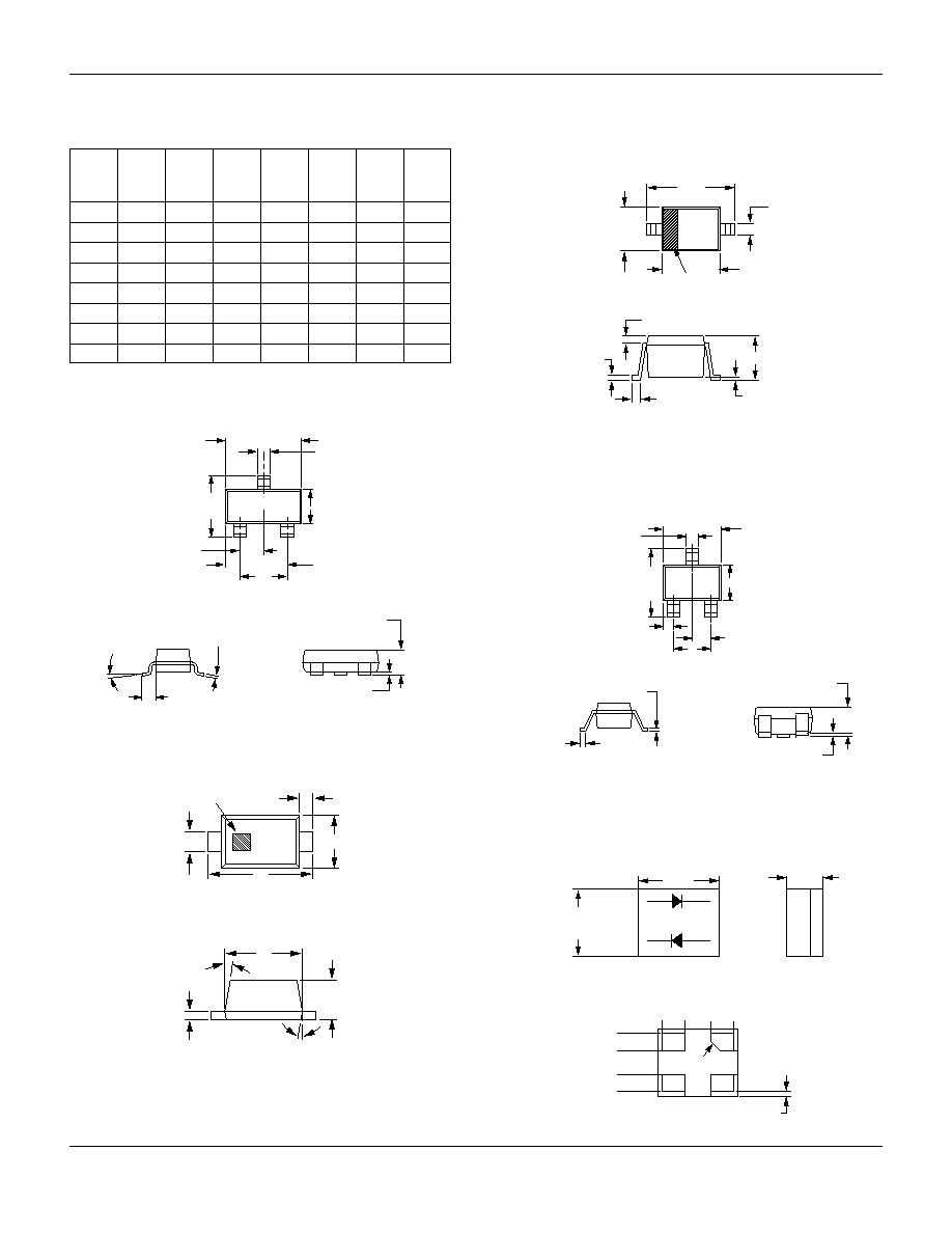
SOT-23
3
2
1
0.035 (0.89 mm) MIN.
0.044 (1.12 mm) MAX.
0.0005 (0.01 mm) MIN.
0.004 (0.10 mm) MAX.
0.012 (0.30 mm) MIN.
0.020 (0.50 mm) MAX.
0.003 (0.080 mm) MIN.
0.008 (0.20 mm) MAX.
8° MAX.
0.022 (0.55 mm) REF.
0.110 (2.80 mm) MIN.
0.120 (3.04 mm) MAX.
0.083 (2.10 mm) MIN.
0.104 (2.64 mm) MAX.
0.037 (0.95 mm) REF.
0.047 (1.20 mm) MIN.
0.055 (1.40 mm) MAX.
0.076 (1.92 mm) REF.
0.020 (0.51 mm) REF.
SC-79
0.060 (1.50 mm) MIN.
0.067 (1.70 mm) MAX.
0.010
(0.25 mm) MIN.
0.014
(0.35 mm) MAX.
0.043 (1.10 mm) MIN.
0.051 (1.30 mm) MAX.
0.020
(0.50 mm) MIN.
0.028
(0.70 mm) MAX.
0.003
(0.07 mm) MIN.
0.008
(0.20 mm) MAX.
10° MAX.
10° MAX.
0.028
(0.70 mm) MIN.
0.035
(0.90 mm) MAX.
0.006 (0.15 mm) MIN.
CATHODE
INDICATOR
1
2
SOD-323
0.090 (2.30 mm) MIN.
0.108 (2.74 mm) MAX.
0.045 (1.15 mm) MIN.
0.053 (1.35 mm) MAX.
0.050
(1.25 mm) MAX.
0.006
(0.15 mm) TYP.
0.008 (0.20 mm) NOM.
0.004 (0.10 mm) MAX.
0.010 (0.25 mm) MIN.
0.010
(0.25 mm) MIN.
0.016
(0.40 mm) MAX.
0.063 (1.60 mm) MIN.
0.071 (1.80 mm) MAX.
CATHODE
INDICATOR
2
1
SC-70
3
2
1
0.031 (0.80 mm) MIN.
0.039 (1.00 mm) MAX.
0.000 (0.00 mm) MIN.
0.004 (0.10 mm) MAX.
0.010 (0.25 mm) MIN.
0.016 (0.40 mm) MAX.
0.071 (1.80 mm) MIN.
0.087 (2.20 mm) MAX.
0.071 (1.80 mm) MIN.
0.094 (2.40 mm) MAX.
0.045 (1.15 mm) MIN.
0.053 (1.35 mm) MAX.
0.026 (0.65 mm) REF.
0.051 (1.30 mm) REF.
0.004 (0.10 mm) MIN.
0.007 (0.18 mm) MAX.
0.004 (0.10 mm) MIN.
0.012 (0.30 mm) MAX.
0.014 (0.35 mm) REF.
R
R
R
R
R
R
R
I
F
-55°C
-40°C
-15°C
+25°C
+65°C
+85°C +100°C
(mA)
(
)
(
)
(
)
(
)
(
)
(
)
(
)
0.02
9.92
9.68
9.30
8.95
8.95
9.01
9.12
0.10
3.90
3.86
3.79
3.80
3.85
3.94
4.03
0.30
2.32
2.33
2.30
2.33
2.35
2.43
2.49
0.50
1.91
1.93
1.90
1.92
1.92
1.99
2.05
1.00
1.54
1.55
1.52
1.53
1.50
1.56
1.61
10.00
0.95
0.96
0.91
0.90
0.82
0.85
0.89
20.00
0.86
0.87
0.82
0.81
0.73
0.75
0.79
100.00
0.72
0.73
0.70
0.68
0.59
0.62
0.65
Resistance vs. Temperature @ 500 MHz
LGA
PIN 2
PIN 3
PIN 1
PIN 1
PIN 3
PIN 2
PIN 4
(1.03)
(0.73)
(0.30)
(0.00)
PIN 4
0.058 (1.47 mm)
0.054 (1.39 mm)
0.028 (0.70 mm)
0.023 (0.58 mm)
SIDE VIEW
TOP VIEW
0.048 (1.23 mm)
0.044 (1.13 mm)
(0.138 x 45)
(1.27)
(0.87)
(0.40)
(0.00)
BOTTOM VIEW
(0.076) ALL AROUND