SL74LS06
System Logic
Semiconductor
SLS
Hex Inverted Buffers with
Open-Collector Outputs
This device contains hex inverted buffers with open-collector. It
performs the Boolean function Y=A in positive Logic.
∑
High Output Voltage (30 V)
∑
High Speed ( t
PD
= 8.5 ns typical)
∑
Low Power Dissipation (P
D
= 18 mW per Gate)
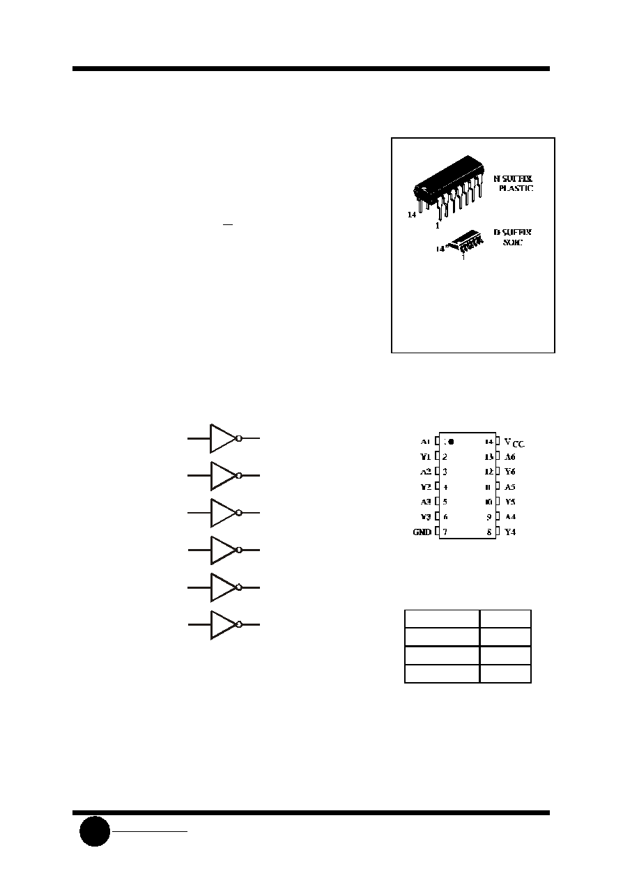
ORDERING INFORMATION
SL74LS06N Plastic
SL74LS06D SOIC
T
A
= 0
∞
to 70
∞
C for all
packages
LOGIC DIAGRAM
A1
A3
A5
A2
A4
A6
Y1
Y3
Y5
Y2
Y4
Y6
11
4
6
1
3
5
9
13
2
8
10
12
PIN 14 =V
CC
PIN 7 = GND
PIN ASSIGNMENT
FUNCTION TABLE
Inputs
Output
A
Y
H
L
L
H
SL74LS06
System Logic
Semiconductor
SLS
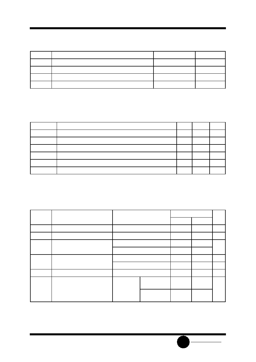
MAXIMUM RATINGS
*
Symbol
Parameter
Value
Unit
V
CC
Supply Voltage
7.0
V
V
IN
Input Voltage
5.5
V
V
OUT
Output Voltage
30
V
Tstg
Storage Temperature Range
-65 to +150
∞
C
*
Maximum Ratings are those values beyond which damage to the device may occur.
Functional operation should be restricted to the Recommended Operating Conditions.
RECOMMENDED OPERATING CONDITIONS
Symbol
Parameter
Min
Max
Unit
V
CC
Supply Voltage
4.75
5.25
V
V
IH
High Level Input Voltage
2.0
V
V
IL
Low Level Input Voltage
0.8
V
V
OH
High Level Output Voltage
30
V
I
OL
Low Level Output Current
40
mA
T
A
Ambient Temperature Range
0
+70
∞
C
DC ELECTRICAL CHARACTERISTICS
over full operating conditions
Guaranteed Limit
Symbol
Parameter
Test Conditions
Min
Max
Unit
V
IK
Input Clamp Voltage
V
CC
= min, I
IN
= -18 mA
-1.5
V
I
OH
High Level Output Current
V
CC
= min, V
OH
= max
250
µ
A
V
OL
Low Level Output Voltage
V
CC
= min, I
OL
= 16 mA
0.4
V
V
CC
= min, I
OL
= 40 mA
0.7
I
IH
High Level Input Current
V
CC
= max, V
IN
= 2.7 V
20
µ
A
V
CC
= max, V
IN
= 5.5 V
1
mA
I
IL
Low Level Input Current
V
CC
= max, V
IN
= 0.4 V
-0.2
mA
I
CC
Supply Current
V
CC
= max
Total with
outputs high
18
mA
Total with
outputs low
60
SL74LS06
System Logic
Semiconductor
SLS
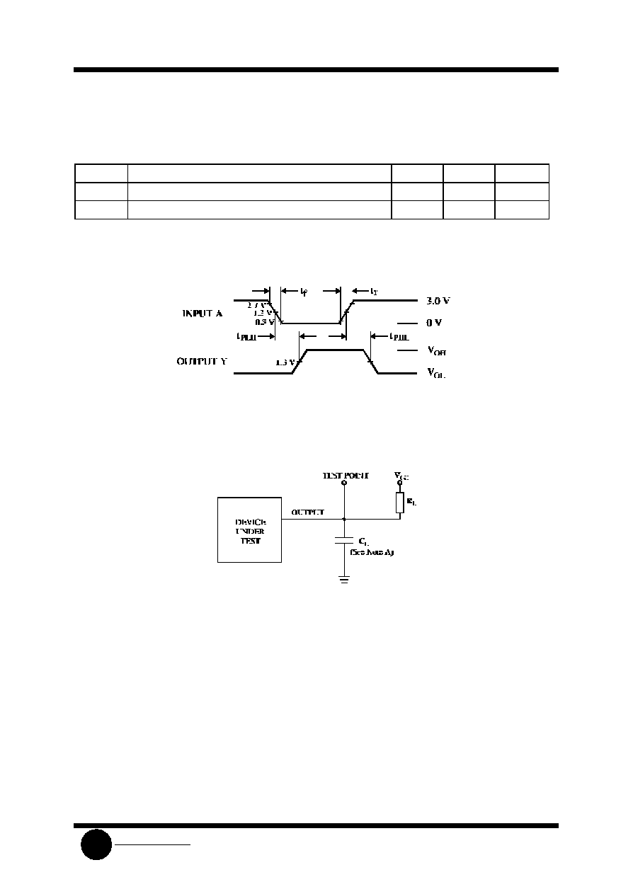
AC ELECTRICAL CHARACTERISTICS
(T
A
= 25
∞
C, V
CC
= 5.0 V, C
L
= 15 pF,
R
L
= 110
, t
r
= 15 ns, t
f
= 6.0 ns)
Symbol
Parameter
Min
Max
Unit
t
PLH
Propagation Delay, Input A to Output Y
15
ns
t
PHL
Propagation Delay, Input A to Output Y
20
ns
Figure 1. Switching Waveforms
NOTE A. C
L
includes probe and jig capacitance.
Figure 2. Test Circuit