 | –≠–ª–µ–∫—Ç—Ä–æ–Ω–Ω—ã–π –∫–æ–º–ø–æ–Ω–µ–Ω—Ç: SL2411 | –°–∫–∞—á–∞—Ç—å:  PDF PDF  ZIP ZIP |
SL2411
System Logic
Semiconductor
SLS
Tone Ringer
The SL2411 is a bipolar integrated circuit designed for telephone bell
replacement.
∑
Designed for Telephone Bell Replacement
∑
Low Curent Drain
∑
Adjustable 2-frequency Tone
∑
Adjustable Warbling Rate
∑
Extension Tone Ringer Modules
∑
Alarms or Other Alerting Devices
∑
Adjustable for Reduced Supply Initiation Current.
∑
Built-in hysteresis prevents false triggering and rotary dial `Chirps'
ORDERING INFORMATION
SL2411N Plastic
SL2411D SOIC
T
A
= -45
∞
to 65
∞
C
for package
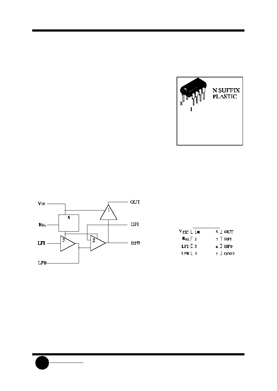
PIN ASSIGNMENT
LOGIC DIAGRAM
PIN 1 = V
CC
PIN 5 = GND
1. Output amplifier
2. High frequency oscillator
3. Low frequency oscillator
4. Hysteresis regulator
(Regulator circuit has built-in hysteresis to prevent false
triggering and rotary dial "Chirps")
SL2411
System Logic
Semiconductor
SLS
PIN DESCRIPTION
NAME
PIN
DESCRIPTION
V
CC
1
Positive power supply.
R
SL
2
External resistor
LFI
3
Input low frequency oscillator
LF0
4
Output low frequency oscillator
GND
5
Negative power supply
HF0
6
High frequency oscillator output
HFI
7
High frequency oscillator input
OUT
8
Tone output
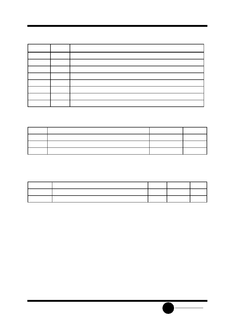
MAXIMUM RATINGS
*
Symbol
Parameter
Value
Unit
V
CC
DC Supply Voltage (Referenced to GND)
to +30.0
V
P
D
Power Dissipation in Still Air, Plastic DIP
400
mW
Tstg
Storage Temperature
-65 to +150
∞
C
*
Maximum Ratings are those values beyond which damage to the device may occur.
Functional operation should be restricted to the Recommended Operating Conditions.
RECOMMENDED OPERATING CONDITIONS
Symbol
Parameter
Min
Max
Unit
V
CC
DC Supply Voltage (Referenced to GND)
13.0
29.0
V
T
A
Operating Temperature
-45
+65
∞
C
This device contains protection circuitry to guard against damage due to high static voltages or electric
fields. However, precautions must be taken to avoid applications of any voltage higher than maximum rated
voltages to this high-impedance circuit. For proper operation, V
IN
and V
OUT
should be constrained to the range
GND
(V
IN
or V
OUT
)
V
CC
.
Unused inputs must always be tied to an appropriate logic voltage level (e.g., either GND or V
CC
).
Unused outputs must be left open.

SL2411
System Logic
Semiconductor
SLS
ELECTRICAL CHARACTERISTICS
(Voltages Referenced to GND, T
A
= -45 to +65
∞
C)
Guaranteed Limits
Symbol
Parameter
Test Conditions
Min
Typ
Max
Unit
V
SI
Initiation Supply Voltage
(1)
See Figure 1
16.8
21.2
V
I
SI
Initiation Supply Current
(1)
1.4
4.2
mA
V
SUS
Sustaining Voltage (2)
See Figure 1
9.5
12.2
V
I
SUS
Sustaining Current (2)
No Load V
CC
=V
SUS
See Figure 1
0.7
2.5
mA
V
OH
High-Level Output
Voltage
V
CC
=21V, I
OH
=-15mA, Pin
6=6V, Pin 7=GND
16.7
21.0
V
V
OL
Low-Level Output
Voltage
V
CC
=21V, I
OL
=15mA, Pin
6=GND, Pin 7=6V
-
1.8
V
I
IN
Maximun Input Leakage
Current (Pin 3)
Pin 3=6V,Pin 4=GND,
V
CC
=21V
-
1.0
µ
A
(Pin 7) Pin 7=6V,Pin 6=GND,
V
CC
=21V
-
1.0
µ
A
f
H1
High Frequency 1
R
3
=191K
,C
3
=6800pF
461
563
Hz
f
H2
High Frequency 2
R
3
=191K
,C
3
=6800pF
576
704
Hz
f
L
Low Frequency
R
2
=165K
,C
2
=0.47
µ
F
9.0
11.0
Hz
Notes:
1. Initiation supply voltage (V
SI
) is the supply voltage required to start the tone ringer oscillating.
2. Sustaining voltage (V
SUS
) is the supply voltage required to maintain oscillation.

SL2411
System Logic
Semiconductor
SLS
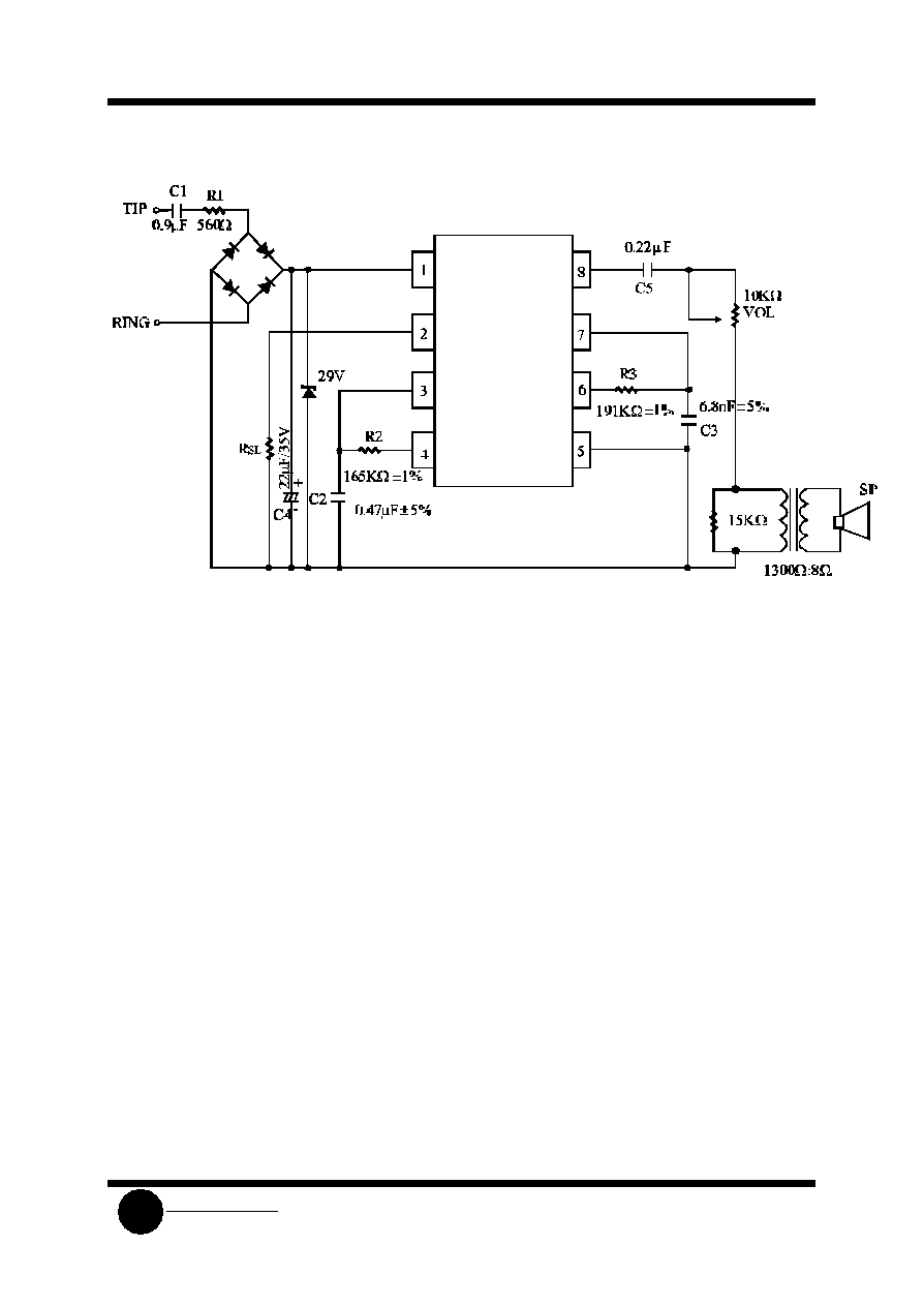
CIRCUIT CURRENT-SUPPLY VOLTAGE (NO LOAD)
Figure 1
SUPPLY CURRENT (NO LOAD) vs. SUPPLY VOLTAGE
Figure 2
SL2411
System Logic
Semiconductor
SLS
APPLICATION CIRCUIT
Figure 3