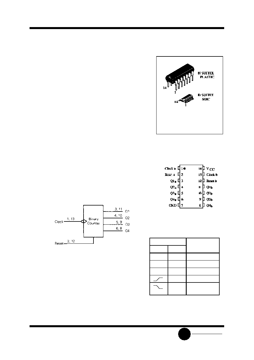
SL74HC393
System Logic
Semiconductor
SLS
Dual 4-Stage Binary Ripple Counter
High-Performance Silicon-Gate CMOS
The SL74HC393 is identical in pinout to the LS/ALS393. The device
inputs are compatible with standard CMOS outputs; with pullup
resistors, they are compatible with LS/ALSTTL outputs.
This device consists of two independent 4-bit binary ripple
counters with parallel outputs from each counter stage. A
˜
256 counter
can be obtained by cascading the two binary counters.
Internal flip-flops are triggered by high-to-low transitions of the
clock input. Reset for the counters is asynchronous and active-high.
State changes of the Q outputs do not occur simultaneously becaue of
internal ripple delays. Therefore, decoded output signals are subject to
decoding spikes and should not be used as clocks or as strobes except
when gated with the Clock of the SL74HC393.
∑
Outputs Directly Interface to CMOS, NMOS, and TTL
∑
Operating Voltage Range: 2.0 to 6.0 V
∑
Low Input Current: 1.0
µ
A
∑
High Noise Immunity Characteristic of CMOS Devices
ORDERING INFORMATION
SL74HC393N Plastic
SL74HC393D SOIC
T
A
= -55
∞
to 125
∞
C for all packages
LOGIC DIAGRAM
PIN 14 =V
CC
PIN 7 = GND
PIN ASSIGNMENT
FUNCTION TABLE
Inputs
Outputs
Clock
Reset
X
H
L
H
L
No Change
L
L
No Change
L
No Change
L
Advance to Next
State
X = don't care
SL74HC393
System Logic
Semiconductor
SLS
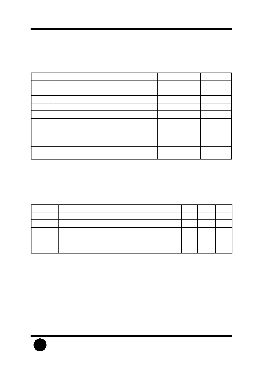
MAXIMUM RATINGS
*
Symbol
Parameter
Value
Unit
V
CC
DC Supply Voltage (Referenced to GND)
-0.5 to +7.0
V
V
IN
DC Input Voltage (Referenced to GND)
-1.5 to V
CC
+1.5
V
V
OUT
DC Output Voltage (Referenced to GND)
-0.5 to V
CC
+0.5
V
I
IN
DC Input Current, per Pin
±
20
mA
I
OUT
DC Output Current, per Pin
±
25
mA
I
CC
DC Supply Current, V
CC
and GND Pins
±
50
mA
P
D
Power Dissipation in Still Air, Plastic DIP+
SOIC Package+
750
500
mW
Tstg
Storage Temperature
-65 to +150
∞
C
T
L
Lead Temperature, 1 mm from Case for 10 Seconds
(Plastic DIP or SOIC Package)
260
∞
C
*
Maximum Ratings are those values beyond which damage to the device may occur.
Functional operation should be restricted to the Recommended Operating Conditions.
+Derating - Plastic DIP: - 10 mW/
∞
C from 65
∞
to 125
∞
C
SOIC Package: : - 7 mW/
∞
C from 65
∞
to 125
∞
C
RECOMMENDED OPERATING CONDITIONS
Symbol
Parameter
Min
Max
Unit
V
CC
DC Supply Voltage (Referenced to GND)
2.0
6.0
V
V
IN
, V
OUT
DC Input Voltage, Output Voltage (Referenced to GND)
0
V
CC
V
T
A
Operating Temperature, All Package Types
-55
+125
∞
C
t
r
, t
f
Input Rise and Fall Time (Figure 1)
V
CC
=2.0 V
V
CC
=4.5 V
V
CC
=6.0 V
0
0
0
1000
500
400
ns
This device contains protection circuitry to guard against damage due to high static voltages or electric
fields. However, precautions must be taken to avoid applications of any voltage higher than maximum rated
voltages to this high-impedance circuit. For proper operation, V
IN
and V
OUT
should be constrained to the range
GND
(V
IN
or V
OUT
)
V
CC
.
Unused inputs must always be tied to an appropriate logic voltage level (e.g., either GND or V
CC
).
Unused outputs must be left open.
SL74HC393
System Logic
Semiconductor
SLS
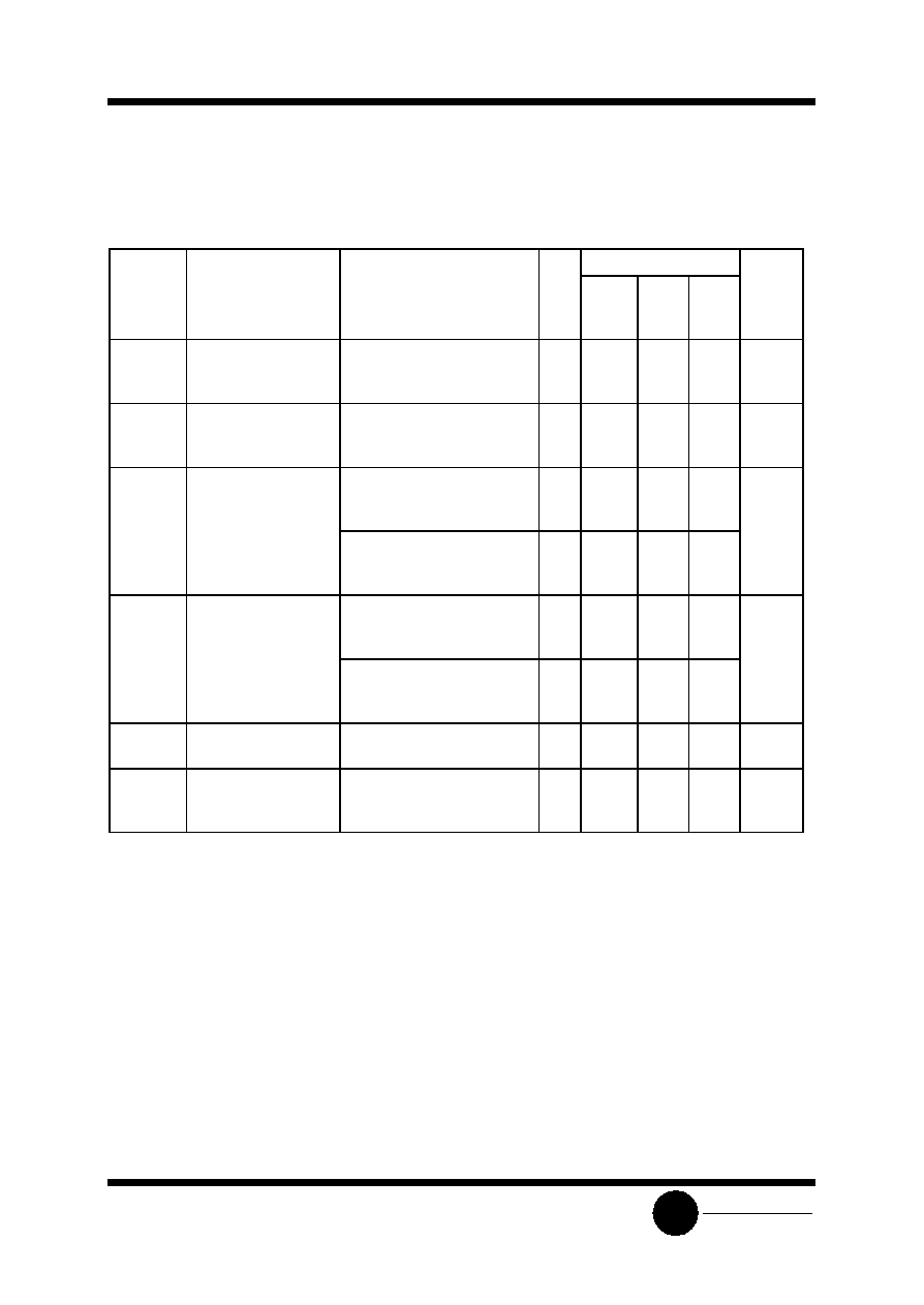
DC ELECTRICAL CHARACTERISTICS
(Voltages Referenced to GND)
V
CC
Guaranteed Limit
Symbol
Parameter
Test Conditions
V
25
∞
C
to
-55
∞
C
85
∞
C
125
∞
C
Unit
V
IH
Minimum High-Level
Input Voltage
V
OUT
=0.1 V or V
CC
-0.1 V
I
OUT
20
µ
A
2.0
4.5
6.0
1.5
3.15
4.2
1.5
3.15
4.2
1.5
3.15
4.2
V
V
IL
Maximum Low -Level
Input Voltage
V
OUT
=0.1 V or V
CC
-0.1 V
I
OUT
20
µ
A
2.0
4.5
6.0
0.3
0.9
1.2
0.3
0.9
1.2
0.3
0.9
1.2
V
V
OH
Minimum High-Level
Output Voltage
V
IN
=V
IH
or V
IL
I
OUT
20
µ
A
2.0
4.5
6.0
1.9
4.4
5.9
1.9
4.4
5.9
1.9
4.4
5.9
V
V
IN
=V
IH
or V
IL
I
OUT
4.0 mA
I
OUT
5.2 mA
4.5
6.0
3.98
5.48
3.84
5.34
3.7
5.2
V
OL
Maximum Low-Level
Output Voltage
V
IN
=V
IH
or V
IL
I
OUT
20
µ
A
2.0
4.5
6.0
0.1
0.1
0.1
0.1
0.1
0.1
0.1
0.1
0.1
V
V
IN
=V
IH
or V
IL
I
OUT
4.0 mA
I
OUT
5.2 mA
4.5
6.0
0.26
0.26
0.33
0.33
0.4
0.4
I
IN
Maximum Input
Leakage Current
V
IN
=V
CC
or GND
6.0
±
0.1
±
1.0
±
1.0
µ
A
I
CC
Maximum Quiescent
Supply Current
(per Package)
V
IN
=V
CC
or GND
I
OUT
=0
µ
A
6.0
8.0
80
160
µ
A
SL74HC393
System Logic
Semiconductor
SLS
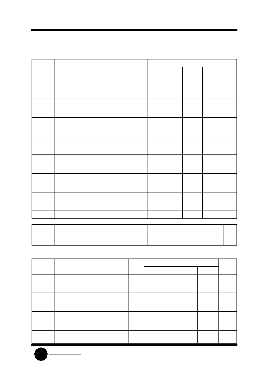
AC ELECTRICAL CHARACTERISTICS
(C
L
=50pF,Input t
r
=t
f
=6.0 ns)
V
CC
Guaranteed Limit
Symbol
Parameter
V
25
∞
C to
-55
∞
C
85
∞
C
125
∞
C Unit
f
max
Maximum Clock Frequency (50% Duty Cycle)
(Figures 1 and 3)
2.0
4.5
6.0
5.4
27
32
4.4
22
26
3.6
18
21
MHz
t
PLH
, t
PHL
Maximum Propagation Delay, Clock to Q1
(Figures 1 and 3)
2.0
4.5
6.0
120
24
20
150
30
26
180
36
31
ns
t
PLH
, t
PHL
Maximum Propagation Delay, Clock to Q2
(Figures 1 and 3)
2.0
4.5
6.0
190
38
32
240
48
41
285
57
48
ns
t
PLH
, t
PHL
Maximum Propagation Delay, Clock to Q3
(Figures 1 and 3)
2.0
4.5
6.0
240
48
41
300
60
51
360
72
61
ns
t
PLH
, t
PHL
Maximum Propagation Delay, Clock to Q4
(Figures 1 and 3)
2.0
4.5
6.0
290
58
49
365
73
62
435
87
74
ns
t
PHL
Maximum Propagation Delay, Reset to any Q
(Figures 2 and 3)
2.0
4.5
6.0
165
33
28
205
41
35
250
50
43
ns
t
TLH
, t
THL
Maximum Output Transition Time, Any Output
(Figures 1 and 3)
2.0
4.5
6.0
75
15
13
95
19
16
110
22
19
ns
C
IN
Maximum Input Capacitance
-
10
10
10
pF
Power Dissipation Capacitance (Per Counter)
Typical @25
∞
C,V
CC
=5.0 V
C
PD
Used to determine the no-load dynamic power
consumption: P
D
=C
PD
V
CC
2
f+I
CC
V
CC
40
pF
TIMING REQUIREMENTS
(C
L
=50pF,Input t
r
=t
f
=6.0 ns)
V
CC
Guaranteed Limit
Symbol
Parameter
V
25
∞
C to-55
∞
C
85
∞
C
125
∞
C
Unit
t
rec
Minimum Recovery Time, Reset
Inactive to Clock (Figure 2)
2.0
4.5
6.0
50
10
9
65
13
11
75
15
13
ns
t
w
Minimum Pulse Width, Clock (Figure
1)
2.0
4.5
6.0
80
16
14
100
20
17
120
24
20
ns
t
w
Minimum Pulse Width, Set
(Figure 2)
2.0
4.5
6.0
125
25
21
155
31
26
190
38
32
ns
t
r
, t
f
Maximum Input Rise and Fall Times
(Figure 1)
2.0
4.5
6.0
1000
500
400
1000
500
400
1000
500
400
ns

SL74HC393
System Logic
Semiconductor
SLS
6.0
400
400
400

SL74HC393
System Logic
Semiconductor
SLS
Figure 1. Switching Waveform
Figure 2. Switching Waveform
Figure 4.Test Circuit
EXPANDED LOGIC DIAGRAM
SL74HC393
System Logic
Semiconductor
SLS
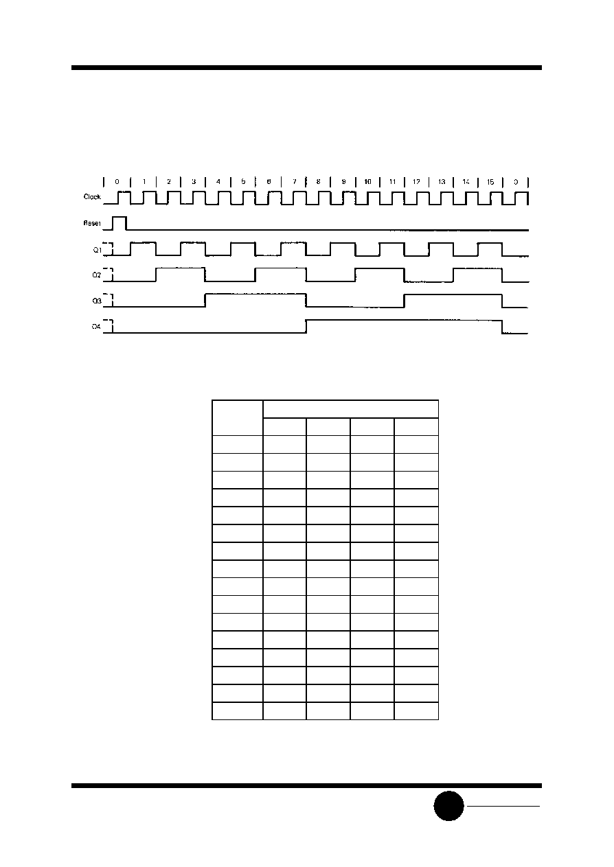
TIMING DIAGRAM
COUNT SEQUENCE
Outputs
Count
Q4
Q3
Q2
Q1
0
L
L
L
L
1
L
L
L
H
2
L
L
H
L
3
L
L
H
H
4
L
H
L
L
5
L
H
L
H
6
L
H
H
L
7
L
H
H
H
8
H
L
L
L
9
H
L
L
H
10
H
L
H
L
11
H
L
H
H
12
H
H
L
L
13
H
H
L
H
14
H
H
H
L
15
H
H
H
H